IO Interfacing ECE 511 Digital System Microprocessor What
























- Slides: 142

I/O Interfacing ECE 511: Digital System & Microprocessor

What we are going to learn in this session: M 68230 Parallel Interface Timer. n Registers in the M 68230. n Port initialization method. n How M 68230 interfaces with various devices. n Delay subroutine. n

The M 6230 Parallel Interface/Timer

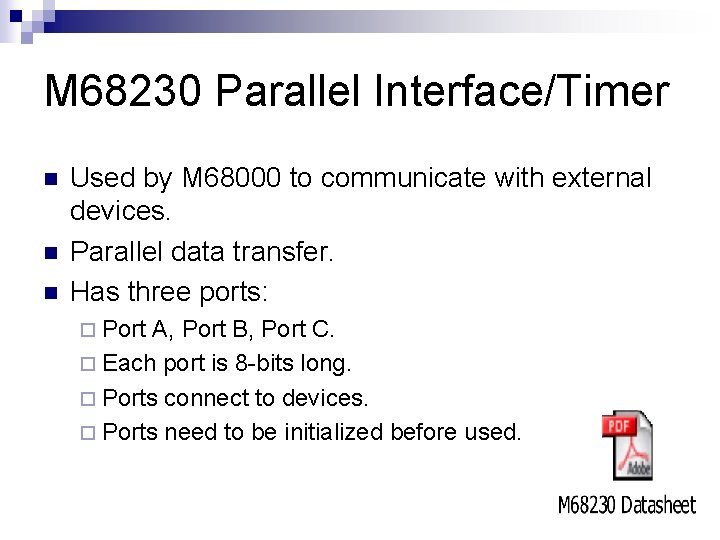
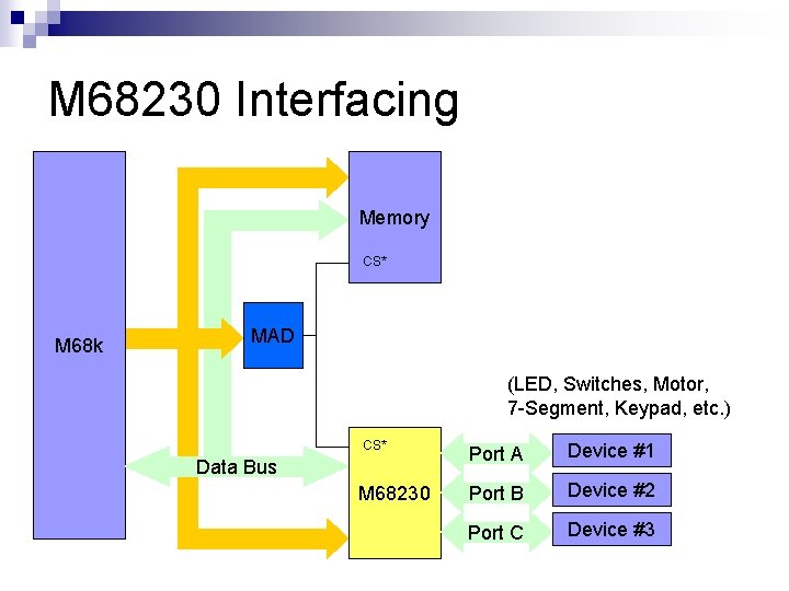
M 68230 Parallel Interface/Timer n n n Used by M 68000 to communicate with external devices. Parallel data transfer. Has three ports: ¨ Port A, Port B, Port C. ¨ Each port is 8 -bits long. ¨ Ports connect to devices. ¨ Ports need to be initialized before used.

M 68230 Interfacing Memory CS* M 68 k MAD (LED, Switches, Motor, 7 -Segment, Keypad, etc. ) CS* Data Bus M 68230 Port A Device #1 Port B Device #2 Port C Device #3

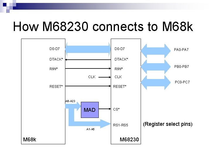
How M 68230 connects to M 68 k D 0 -D 7 DTACK* R/W* CLK PA 0 -PA 7 PB 0 -PB 7 CLK PC 0 -PC 7 RESET* A 6 -A 23 MAD CS* RS 1 -RS 5 A 1 -A 5 M 68 k M 68230 (Register select pins)

M 68230 Ports

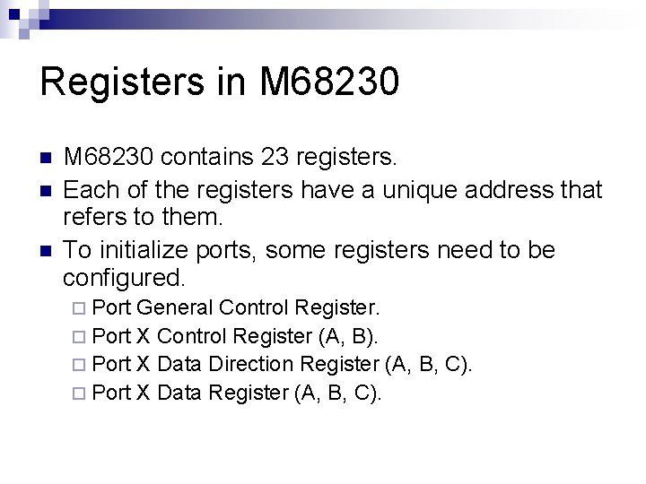
Registers in M 68230 n n n M 68230 contains 23 registers. Each of the registers have a unique address that refers to them. To initialize ports, some registers need to be configured. ¨ Port General Control Register. ¨ Port X Control Register (A, B). ¨ Port X Data Direction Register (A, B, C). ¨ Port X Data Register (A, B, C).

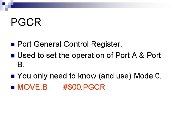
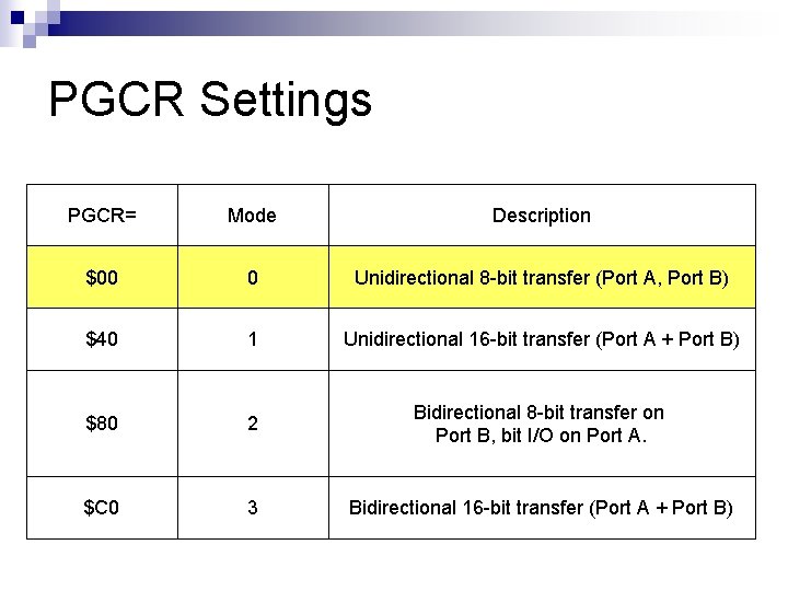
PGCR Port General Control Register. n Used to set the operation of Port A & Port B. n You only need to know (and use) Mode 0. n MOVE. B #$00, PGCR n

PGCR Settings PGCR= Mode Description $00 0 Unidirectional 8 -bit transfer (Port A, Port B) $40 1 Unidirectional 16 -bit transfer (Port A + Port B) $80 2 Bidirectional 8 -bit transfer on Port B, bit I/O on Port A. $C 0 3 Bidirectional 16 -bit transfer (Port A + Port B)

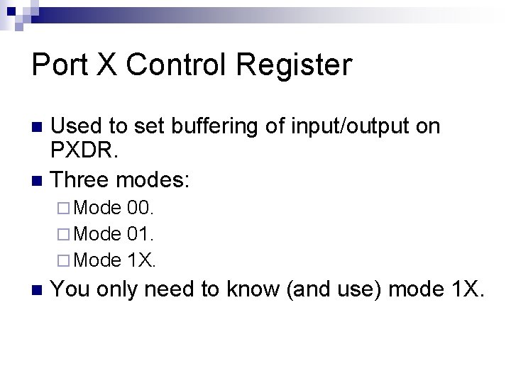
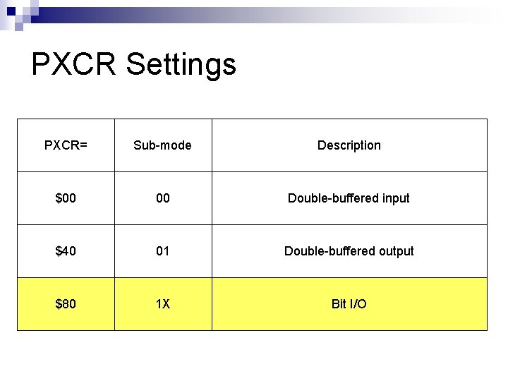
Port X Control Register Used to set buffering of input/output on PXDR. n Three modes: n ¨ Mode 00. ¨ Mode 01. ¨ Mode 1 X. n You only need to know (and use) mode 1 X.

PXCR Settings PXCR= Sub-mode Description $00 00 Double-buffered input $40 01 Double-buffered output $80 1 X Bit I/O

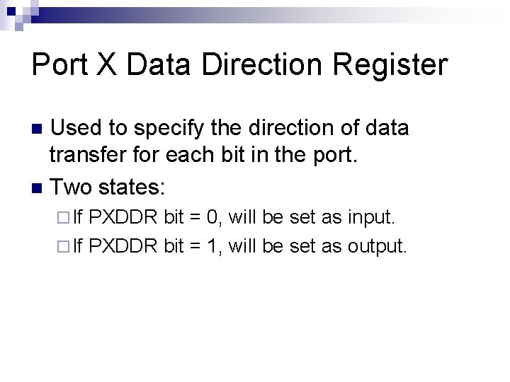
Port X Data Direction Register Used to specify the direction of data transfer for each bit in the port. n Two states: n ¨ If PXDDR bit = 0, will be set as input. ¨ If PXDDR bit = 1, will be set as output.

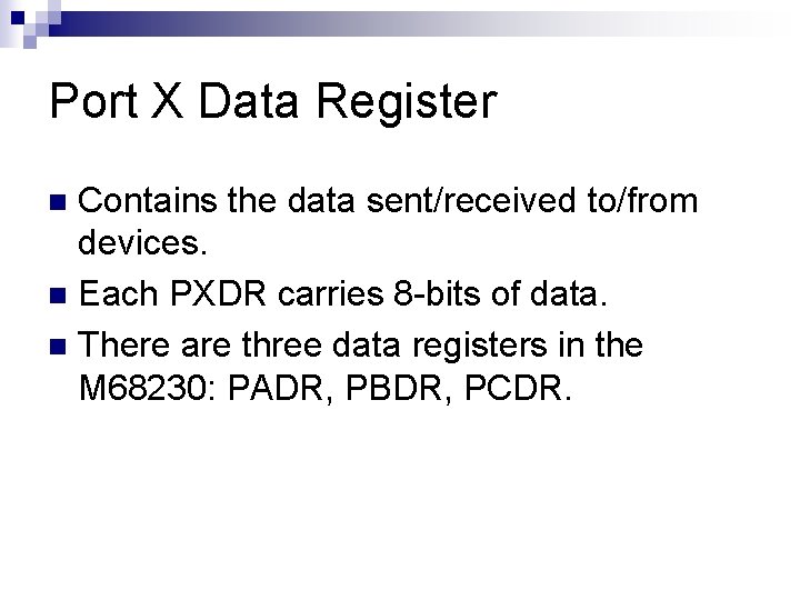
Port X Data Register Contains the data sent/received to/from devices. n Each PXDR carries 8 -bits of data. n There are three data registers in the M 68230: PADR, PBDR, PCDR. n

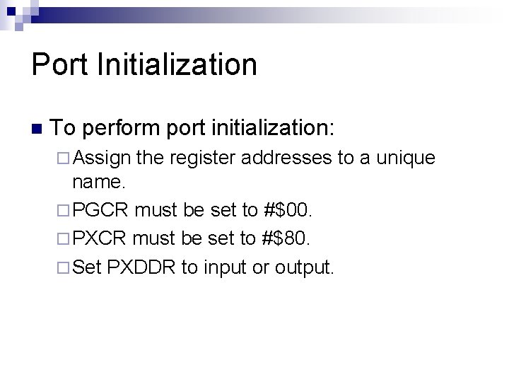
Port Initialization n To perform port initialization: ¨ Assign the register addresses to a unique name. ¨ PGCR must be set to #$00. ¨ PXCR must be set to #$80. ¨ Set PXDDR to input or output.

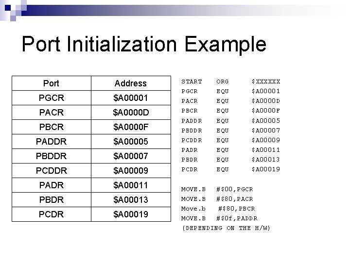
Port Initialization Example Port Address PGCR $A 00001 PACR $A 0000 D PBCR $A 0000 F PADDR $A 00005 PBDDR $A 00007 PCDDR $A 00009 PADR $A 00011 PBDR $A 00013 PCDR $A 00019 START PGCR PACR PBCR PADDR PBDDR PCDDR PADR PBDR PCDR ORG EQU EQU EQU $XXXXXX $A 00001 $A 0000 D $A 0000 F $A 00005 $A 00007 $A 00009 $A 00011 $A 00013 $A 00019 MOVE. B #$00, PGCR MOVE. B #$80, PACR Move. b #$80, PBCR MOVE. B #$0 f, PADDR (DEPENDING ON THE H/W)

68230 Interfacing

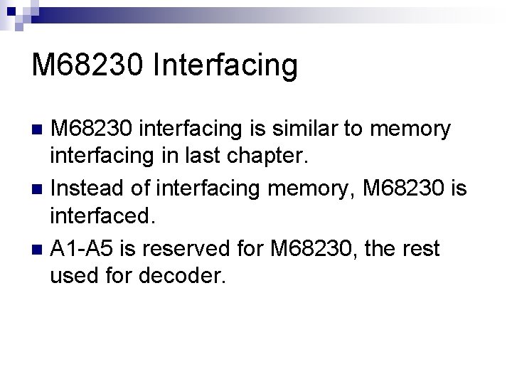
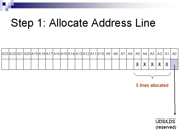
M 68230 Interfacing M 68230 interfacing is similar to memory interfacing in last chapter. n Instead of interfacing memory, M 68230 is interfaced. n A 1 -A 5 is reserved for M 68230, the rest used for decoder. n

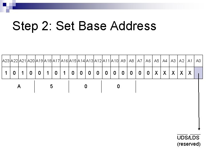
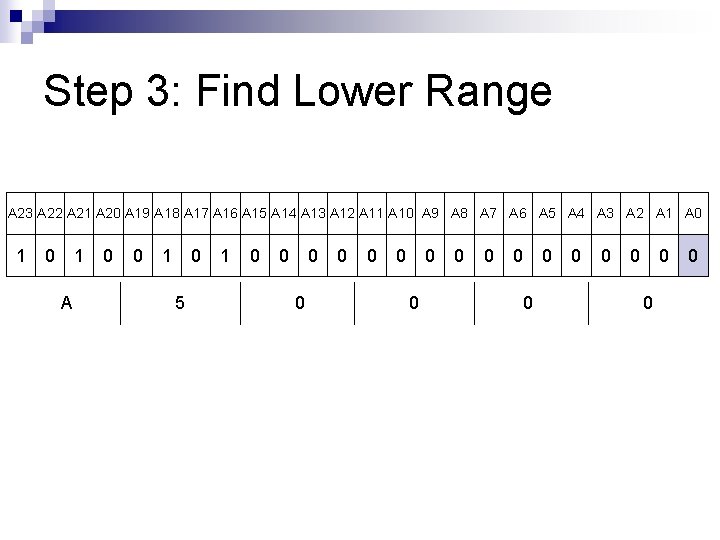
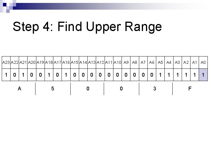
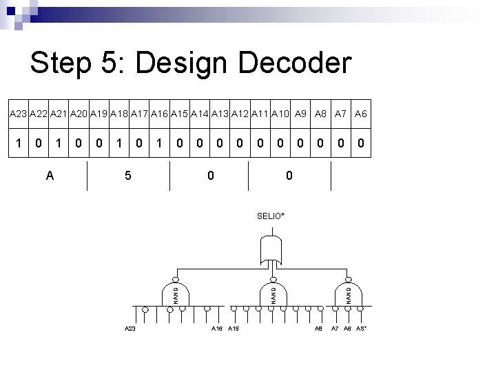
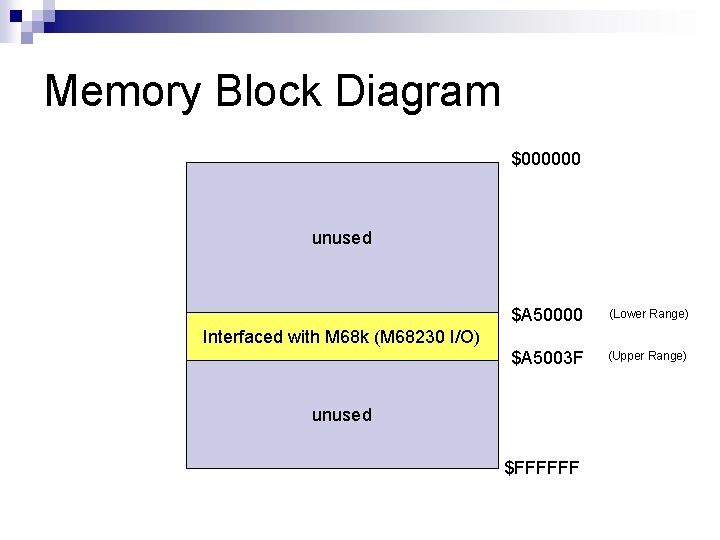
Example: Full Decoding n Interface M 68230 with M 68 k so that its base address is $A 50000.

Discussion n For M 68230 interfacing, 5 lines are automatically reserved for M 68230.

Step 1: Allocate Address Line A 23 A 22 A 21 A 20 A 19 A 18 A 17 A 16 A 15 A 14 A 13 A 12 A 11 A 10 A 9 A 8 A 7 A 6 A 5 A 4 A 3 A 2 A 1 A 0 X X X 5 lines allocated UDS/LDS (reserved)

Step 2: Set Base Address A 23 A 22 A 21 A 20 A 19 A 18 A 17 A 16 A 15 A 14 A 13 A 12 A 11 A 10 A 9 A 8 A 7 A 6 A 5 A 4 A 3 A 2 A 1 A 0 0 1 0 5 1 0 0 0 X X X 0 UDS/LDS (reserved)

Step 3: Find Lower Range A 23 A 22 A 21 A 20 A 19 A 18 A 17 A 16 A 15 A 14 A 13 A 12 A 11 A 10 A 9 A 8 A 7 A 6 A 5 A 4 A 3 A 2 A 1 A 0 0 1 0 5 1 0 0 0 0 0

Step 4: Find Upper Range A 23 A 22 A 21 A 20 A 19 A 18 A 17 A 16 A 15 A 14 A 13 A 12 A 11 A 10 A 9 A 8 A 7 A 6 A 5 A 4 A 3 A 2 A 1 A 0 0 1 0 5 1 0 0 0 1 3 1 1 F 1

Step 5: Design Decoder A 23 A 22 A 21 A 20 A 19 A 18 A 17 A 16 A 15 A 14 A 13 A 12 A 11 A 10 A 9 A 8 A 7 A 6 A 0 0 1 0 5 0 0 0 SELIO* A 23 A 16 A 15 NAND 1 NAND 0 NAND 1 A 8 A 7 A 6 AS*

Memory Block Diagram $000000 unused $A 50000 (Lower Range) $A 5003 F (Upper Range) Interfaced with M 68 k (M 68230 I/O) unused $FFFFFF

Sample Programs

LEDs & Switches

Example 1

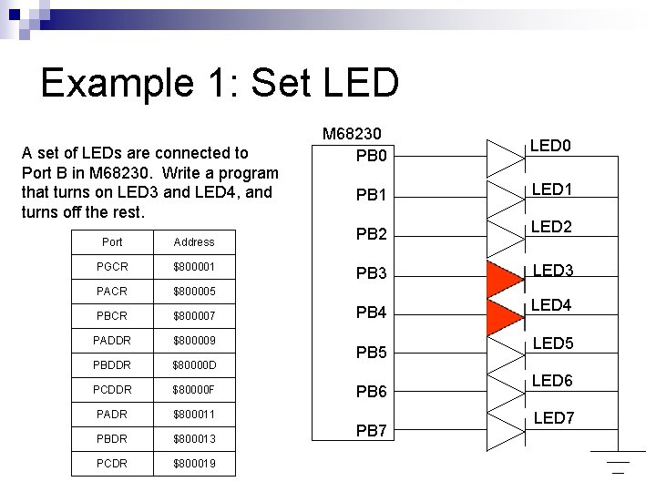
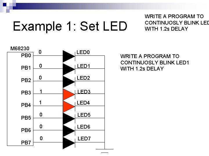
Example 1: Set LED A set of LEDs are connected to Port B in M 68230. Write a program that turns on LED 3 and LED 4, and turns off the rest. Port Address PGCR $800001 PACR $800005 PBCR $800007 PADDR $800009 PBDDR $80000 D PCDDR $80000 F PADR $800011 PBDR $800013 PCDR $800019 M 68230 PB 0 LED 0 PB 1 LED 1 PB 2 LED 2 PB 3 LED 3 PB 4 LED 4 PB 5 PB 6 PB 7 LED 5 LED 6 LED 7

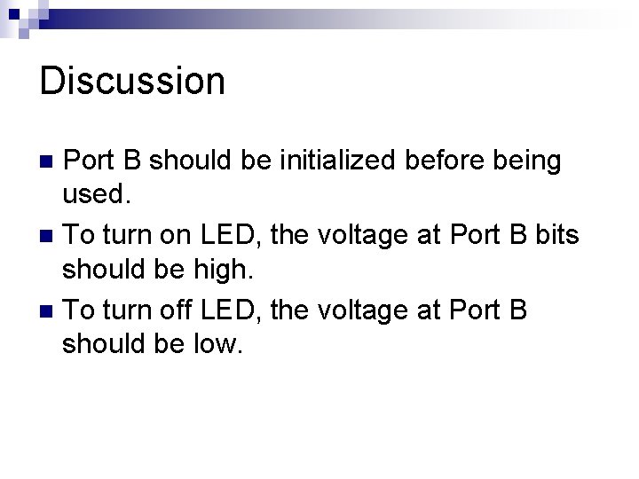
Discussion Port B should be initialized before being used. n To turn on LED, the voltage at Port B bits should be high. n To turn off LED, the voltage at Port B should be low. n

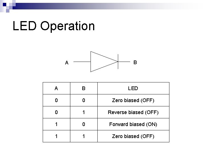
LED Operation B A A B LED 0 0 Zero biased (OFF) 0 1 Reverse biased (OFF) 1 0 Forward biased (ON) 1 1 Zero biased (OFF)

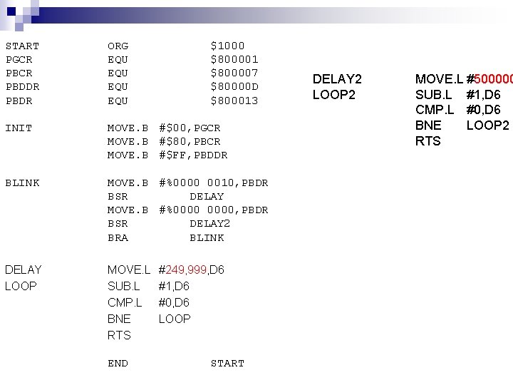
START PGCR PBDDR PBDR ORG EQU EQU INIT MOVE. B #$00, PGCR MOVE. B #$80, PBCR MOVE. B #$FF, PBDDR BLINK MOVE. B #%0000 0010, PBDR BSR DELAY MOVE. B #%0000, PBDR BSR DELAY 2 BRA BLINK DELAY LOOP MOVE. L SUB. L CMP. L BNE RTS END $1000 $800001 $800007 $80000 D $800013 #249, 999, D 6 #1, D 6 #0, D 6 LOOP START DELAY 2 LOOP 2 MOVE. L #500000 SUB. L #1, D 6 CMP. L #0, D 6 BNE LOOP 2 RTS

Example 1: Set LED M 68230 PB 0 0 LED 0 PB 1 0 LED 2 1 LED 3 1 LED 4 0 LED 5 0 LED 6 0 LED 7 PB 2 PB 3 PB 4 PB 5 PB 6 PB 7 WRITE A PROGRAM TO CONTINUOSLY BLINK LED WITH 1. 2 s DELAY WRITE A PROGRAM TO CONTINUOSLY BLINK LED 1 WITH 1. 2 s DELAY

Example 2

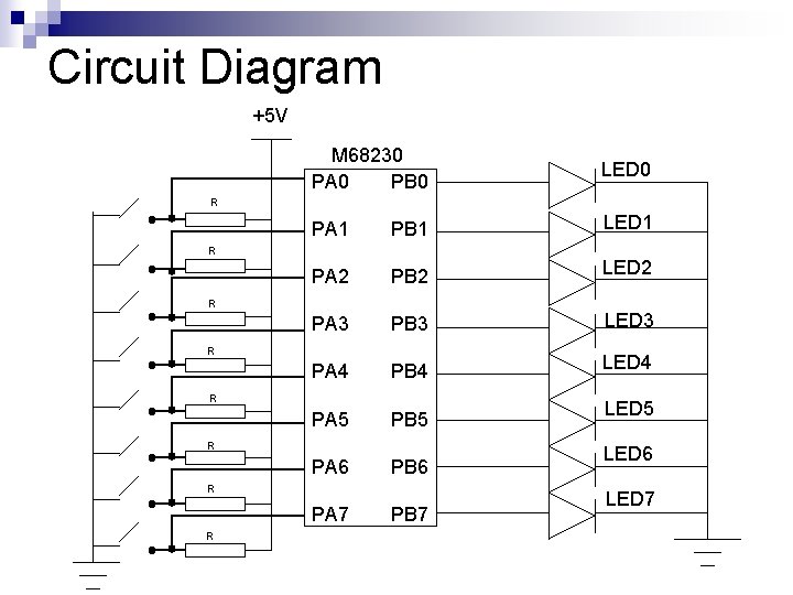
Example 2: Read Switches & Output to LED n A set of switches are connected to Port A, and a set of LEDs are connected to Port B in M 68230. Write a program that reads the value in the switches and turns on the respective LEDs.

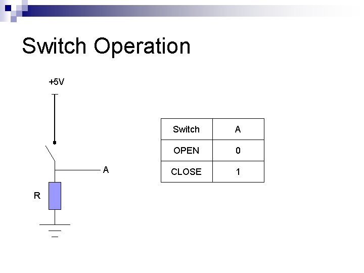
Switch Operation +5 V A R Switch A OPEN 0 CLOSE 1

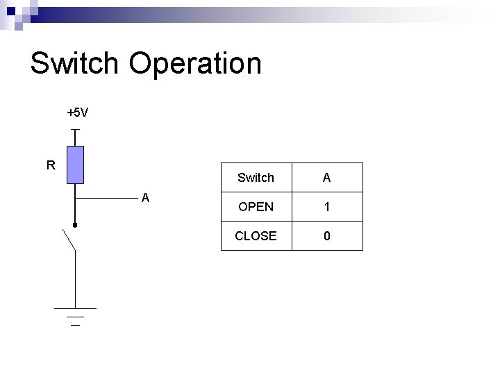
Switch Operation +5 V R A Switch A OPEN 1 CLOSE 0

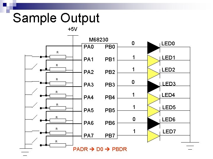
Circuit Diagram +5 V M 68230 PA 0 PB 0 LED 0 PA 1 PB 1 LED 1 PA 2 PB 2 LED 2 PA 3 PB 3 LED 3 PA 4 PB 4 LED 4 PA 5 PB 5 PA 6 PB 6 R R R R PA 7 R PB 7 LED 5 LED 6 LED 7

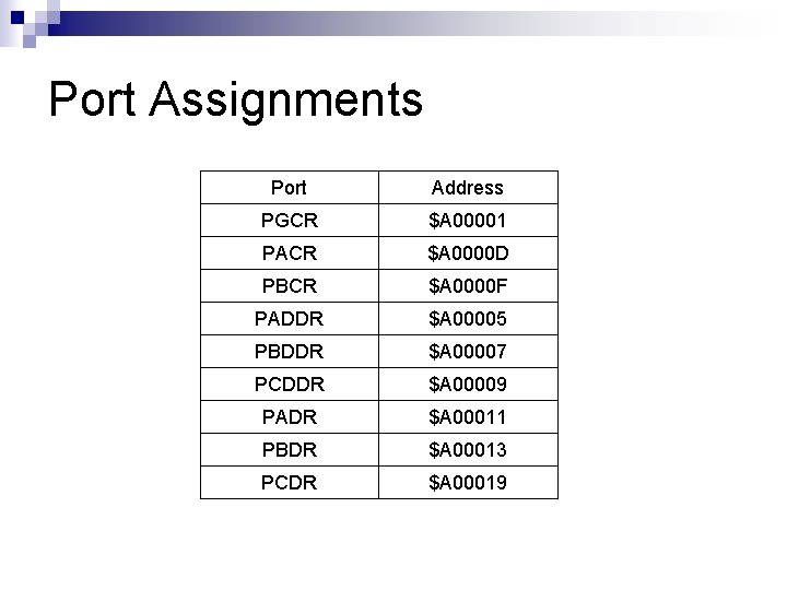
Port Assignments Port Address PGCR $A 00001 PACR $A 0000 D PBCR $A 0000 F PADDR $A 00005 PBDDR $A 00007 PCDDR $A 00009 PADR $A 00011 PBDR $A 00013 PCDR $A 00019

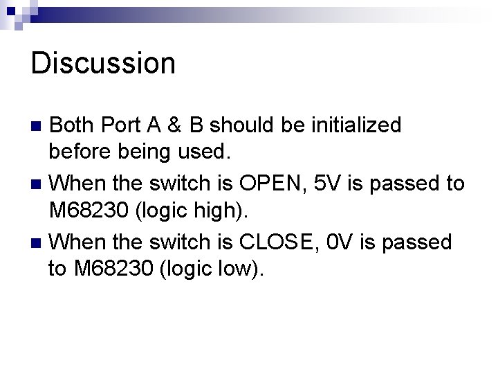
Discussion Both Port A & B should be initialized before being used. n When the switch is OPEN, 5 V is passed to M 68230 (logic high). n When the switch is CLOSE, 0 V is passed to M 68230 (logic low). n

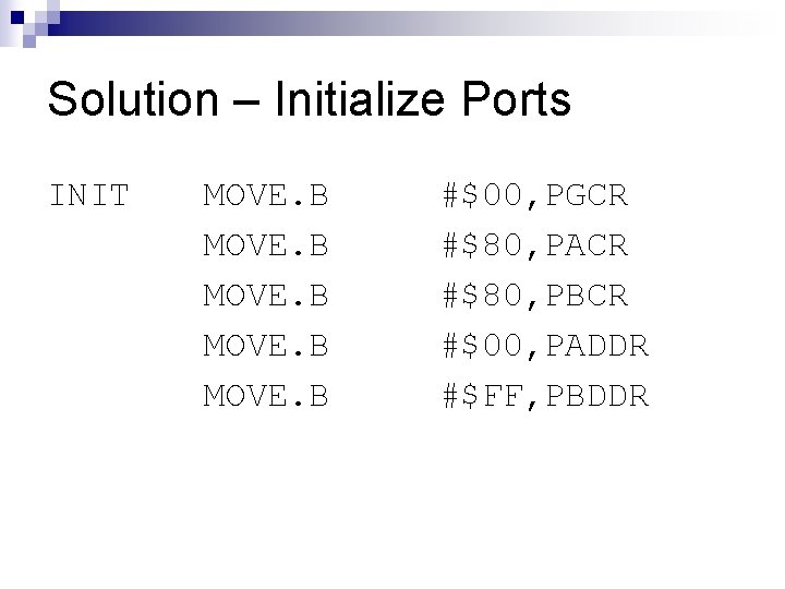
Solution – Initialize Ports INIT MOVE. B #$00, PGCR #$80, PACR #$80, PBCR #$00, PADDR #$FF, PBDDR

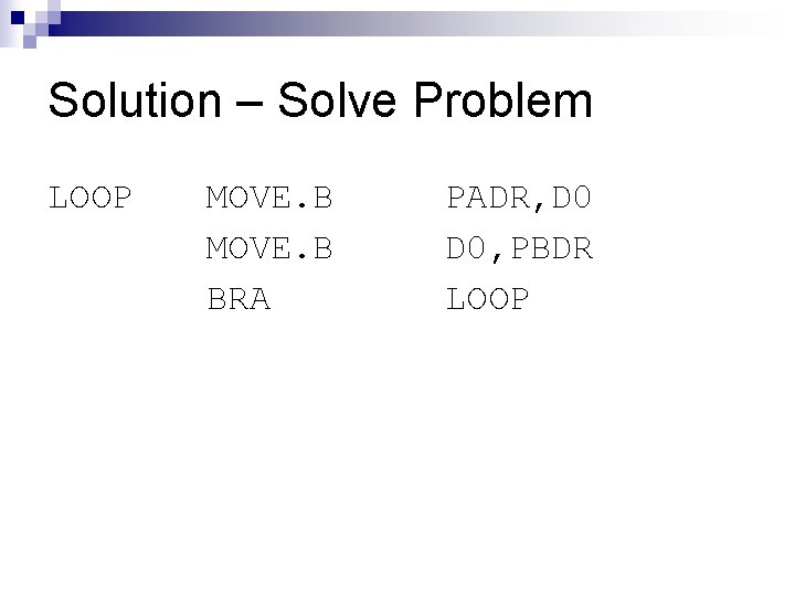
Solution – Solve Problem LOOP MOVE. B BRA PADR, D 0, PBDR LOOP

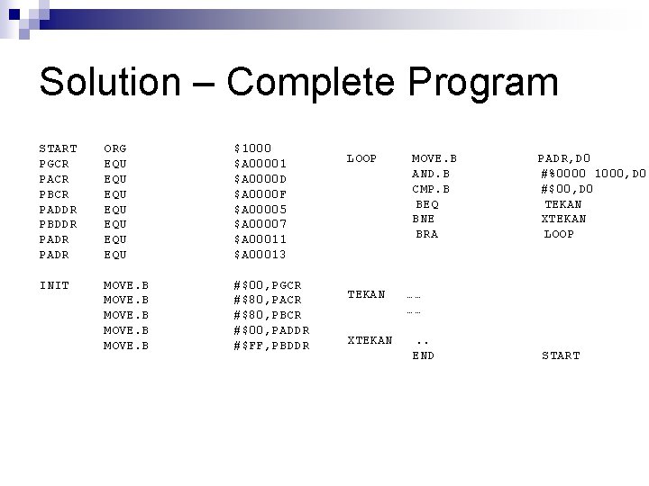
Solution – Complete Program START PGCR PACR PBCR PADDR PBDDR PADR ORG EQU EQU $1000 $A 00001 $A 0000 D $A 0000 F $A 00005 $A 00007 $A 00011 $A 00013 INIT MOVE. B #$00, PGCR #$80, PACR #$80, PBCR #$00, PADDR #$FF, PBDDR LOOP TEKAN XTEKAN MOVE. B AND. B CMP. B BEQ BNE BRA PADR, D 0 #%0000 1000, D 0 #$00, D 0 TEKAN XTEKAN LOOP …… ……. . END START

Sample Output +5 V M 68230 PA 0 PB 0 0 LED 0 PA 1 PB 1 1 LED 1 PA 2 PB 2 1 LED 2 PA 3 PB 3 0 LED 3 PA 4 PB 4 1 LED 4 PA 5 PB 5 1 LED 5 PA 6 PB 6 0 LED 6 1 LED 7 R R R R PA 7 PB 7 R PADR D 0 PBDR

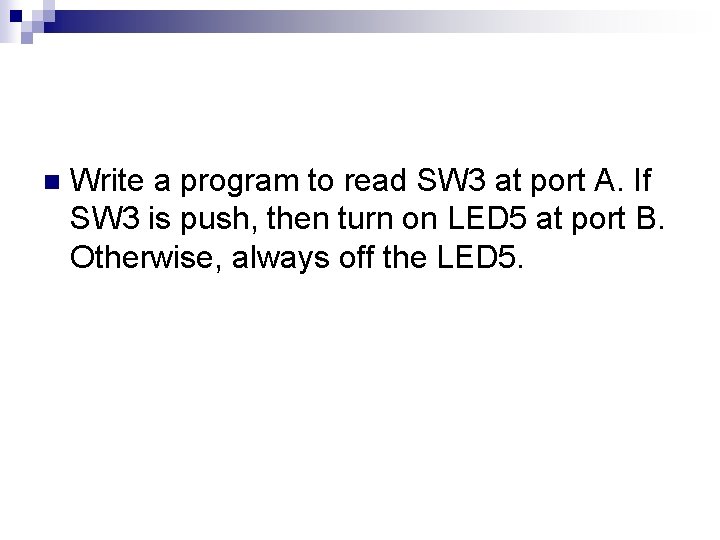
n Write a program to read SW 3 at port A. If SW 3 is push, then turn on LED 5 at port B. Otherwise, always off the LED 5.

7 -Segment

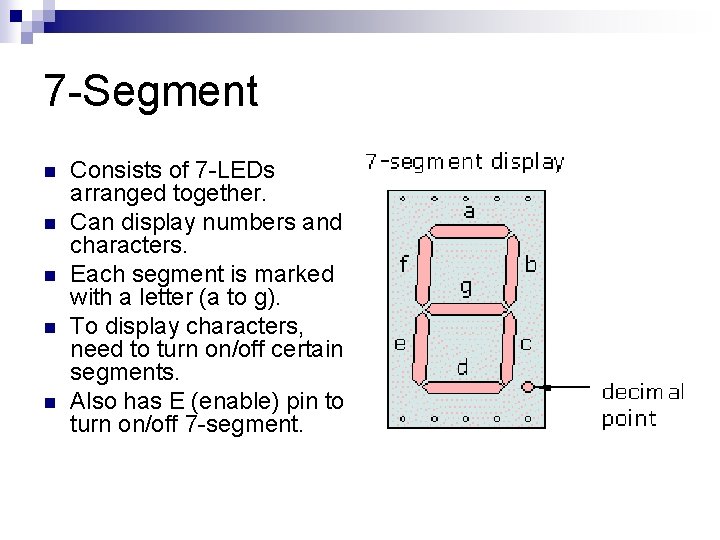
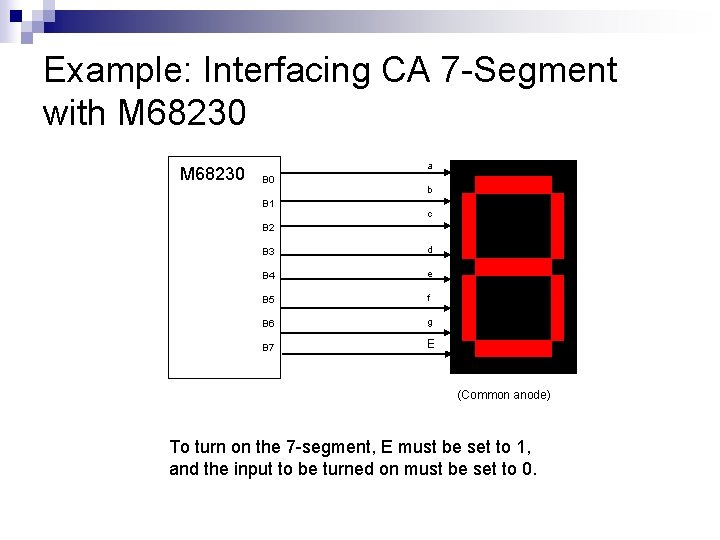
7 -Segment n n n Consists of 7 -LEDs arranged together. Can display numbers and characters. Each segment is marked with a letter (a to g). To display characters, need to turn on/off certain segments. Also has E (enable) pin to turn on/off 7 -segment.

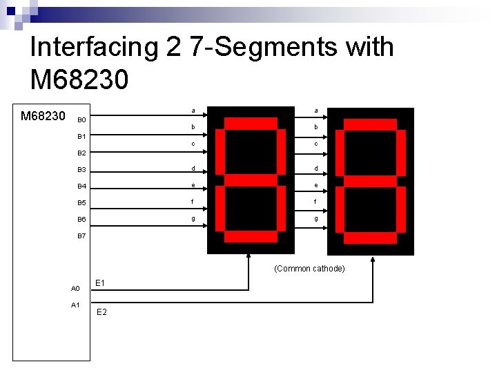
Interfacing 7 -Segment with M 68230 To interface with M 68230, each segment (a to g) is connected to a port in M 68230. n The E signal must also be connected to a port to enable/disable the 7 -segment. n

7 -Segment Types n There are two types of 7 -segment displays: ¨ Common cathode. ¨ Common anode. n Each type differs in how they behave with certain inputs.

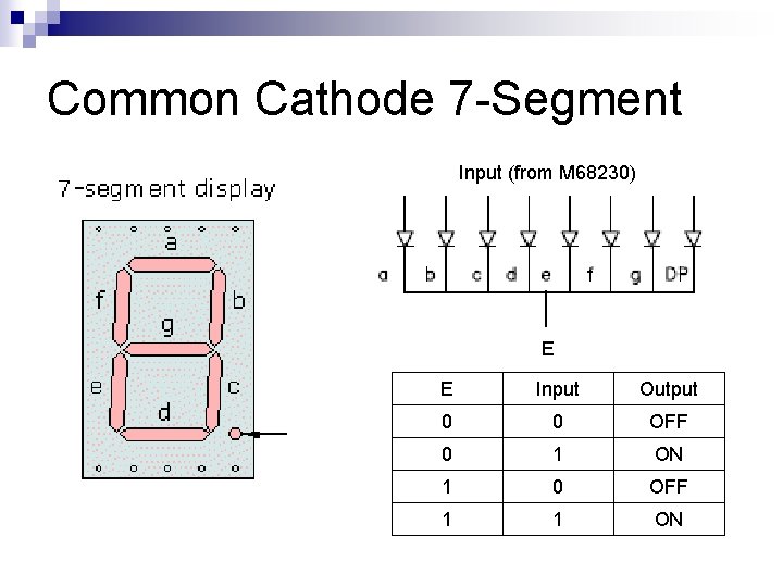
Common Cathode 7 -Segment Input (from M 68230) E E Input Output 0 0 OFF 0 1 ON 1 0 OFF 1 1 ON

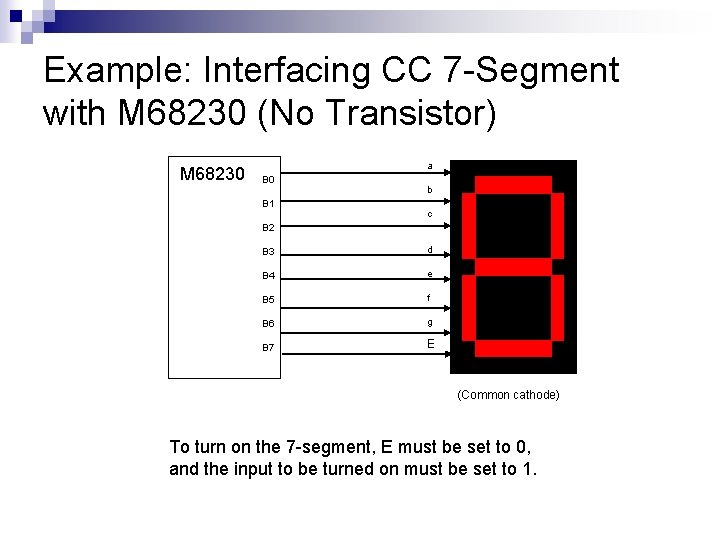
Example: Interfacing CC 7 -Segment with M 68230 (No Transistor) M 68230 a B 0 B 1 b c B 2 B 3 d B 4 e B 5 f B 6 g B 7 E (Common cathode) To turn on the 7 -segment, E must be set to 0, and the input to be turned on must be set to 1.

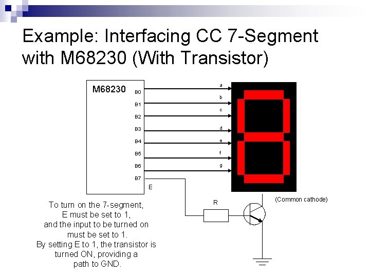
Example: Interfacing CC 7 -Segment with M 68230 (With Transistor) M 68230 a B 0 b B 1 c B 2 B 3 d B 4 e B 5 f B 6 g B 7 E To turn on the 7 -segment, E must be set to 1, and the input to be turned on must be set to 1. By setting E to 1, the transistor is turned ON, providing a path to GND. R (Common cathode)

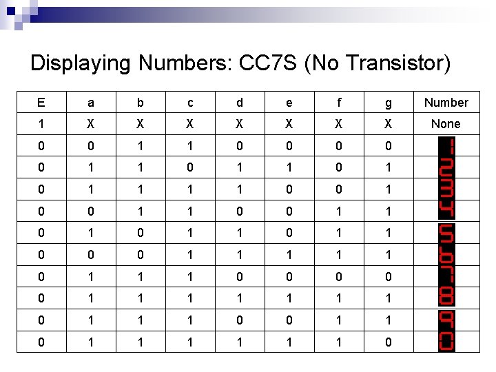
Displaying Numbers: CC 7 S (No Transistor) E a b c d e f g Number 1 X X X X None 0 0 1 1 0 0 1 0 1 2 0 1 1 0 0 1 3 0 0 1 1 4 0 1 1 5 0 0 0 1 1 1 6 0 1 1 1 0 0 7 0 1 1 1 1 8 0 1 1 1 0 0 1 1 9 0 1 1 1 0 0

Displaying Numbers: CC 7 S (with Transistor) E a b c d e f g Number 0 X X X X None 1 1 1 0 0 0 1 1 0 1 2 1 1 1 0 0 1 3 1 0 1 1 0 0 1 1 4 1 1 0 1 1 5 1 0 0 1 1 1 6 1 1 0 0 7 1 1 1 1 8 1 1 0 0 1 1 9 1 1 1 1 0 0

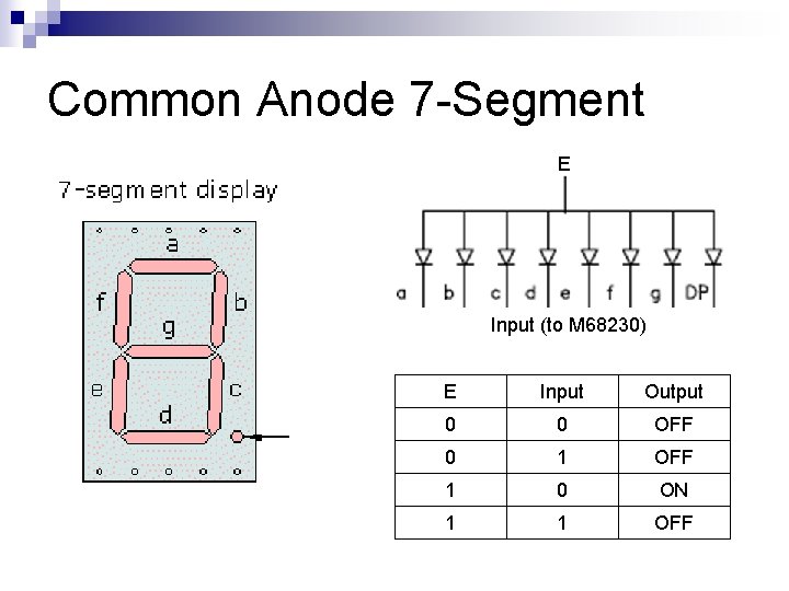
Common Anode 7 -Segment E Input (to M 68230) E Input Output 0 0 OFF 0 1 OFF 1 0 ON 1 1 OFF

Example: Interfacing CA 7 -Segment with M 68230 a B 0 B 1 b c B 2 B 3 d B 4 e B 5 f B 6 g B 7 E (Common anode) To turn on the 7 -segment, E must be set to 1, and the input to be turned on must be set to 0.

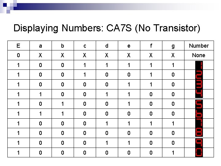
Displaying Numbers: CA 7 S (No Transistor) E a b c d e f g Number 0 X X X X None 1 0 0 1 1 1 0 0 1 0 1 1 0 3 1 1 0 0 4 1 0 0 5 1 1 1 0 0 0 6 1 0 0 0 1 1 7 1 0 0 0 0 8 1 0 0 0 1 1 0 0 9 1 0 0 0 1 1

Example 1

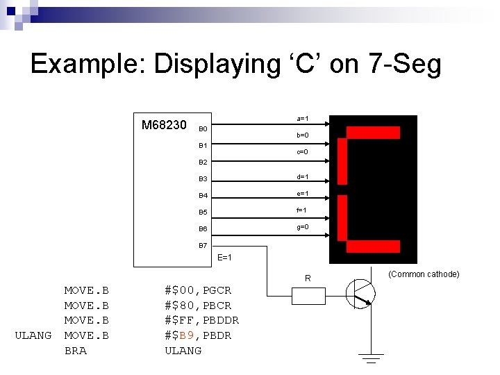
Example: Displaying ‘C’ on 7 -Seg M 68230 a=1 B 0 b=0 B 1 c=0 B 2 B 3 d=1 B 4 e=1 B 5 f=1 B 6 g=0 B 7 E=1 R ULANG MOVE. B BRA #$00, PGCR #$80, PBCR #$FF, PBDDR #$B 9, PBDR ULANG (Common cathode)

Displaying More Numbers/Characters 7 -Segments can also be grouped together to display multiple numbers/characters. n Usually done using a technique called multiplexing. n

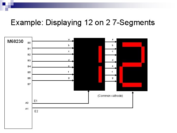
Interfacing 2 7 -Segments with M 68230 a a b b c c B 3 d d B 4 e e B 5 f f B 6 g g B 0 B 1 B 2 B 7 (Common cathode) A 0 A 1 E 2

Example 2

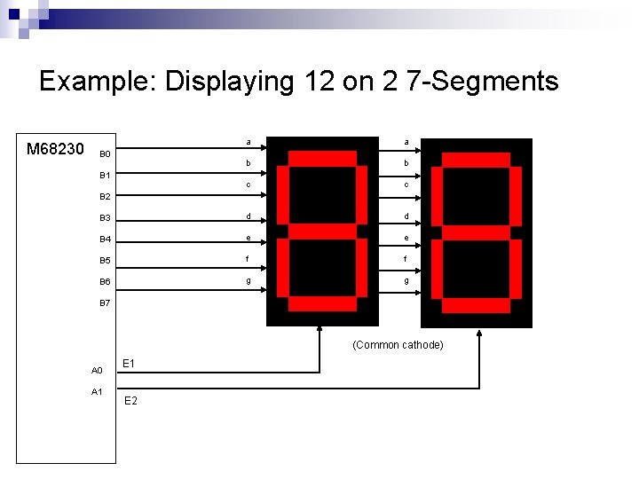
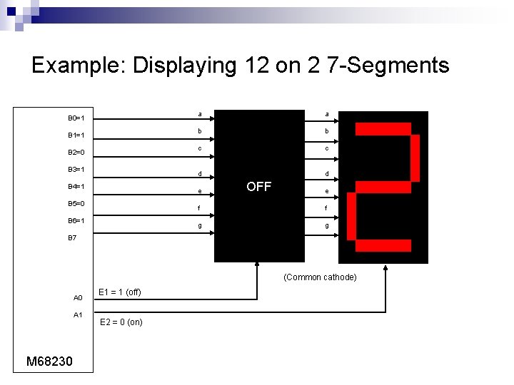
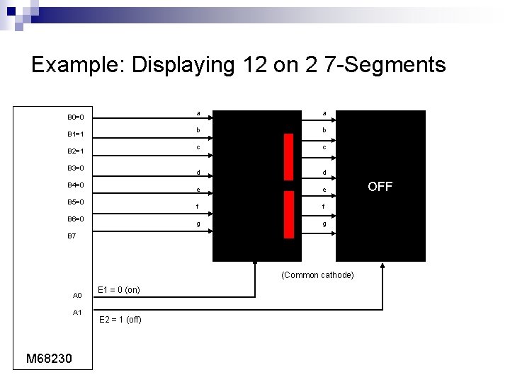
Example: Displaying on Multiple 7 -Segs n Write a program to display ‘ 12’ on 2 7 Segment displays. The circuit diagram is shown.

Example: Displaying 12 on 2 7 -Segments M 68230 a a b b c c B 3 d d B 4 e e B 5 f f B 6 g g B 0 B 1 B 2 B 7 (Common cathode) A 0 A 1 E 2

Step 1: Init Ports MOVE. B #$00, PGCR #$80, PACR #$80, PBCR #$FF, PADDR #$FF, PBDDR

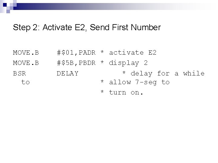
Step 2: Activate E 2, Send First Number MOVE. B BSR to #$01, PADR * activate E 2 #$5 B, PBDR * display 2 DELAY * delay for a while * allow 7 -seg to * turn on.

Example: Displaying 12 on 2 7 -Segments B 0=1 B 1=1 B 2=0 B 3=1 B 4=1 a a b b c c d d e B 5=0 B 6=1 OFF e f f g g B 7 (Common cathode) A 0 A 1 M 68230 E 1 = 1 (off) E 2 = 0 (on)

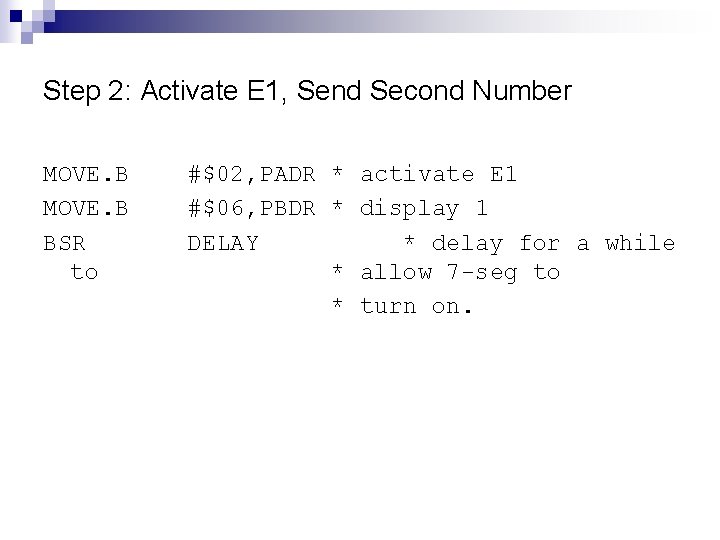
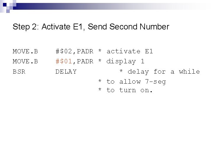
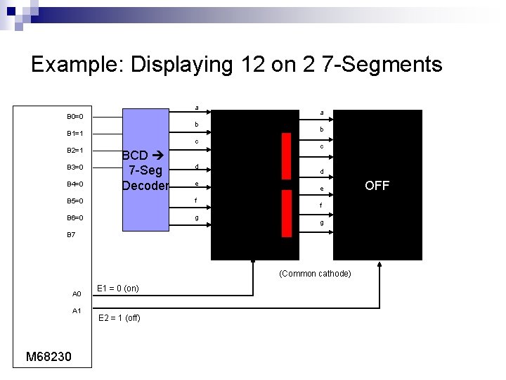
Step 2: Activate E 1, Send Second Number MOVE. B BSR to #$02, PADR * activate E 1 #$06, PBDR * display 1 DELAY * delay for a while * allow 7 -seg to * turn on.

Example: Displaying 12 on 2 7 -Segments B 0=0 B 1=1 B 2=1 B 3=0 B 4=0 B 5=0 B 6=0 a a b b c c d d e e f f g g B 7 (Common cathode) A 0 A 1 M 68230 E 1 = 0 (on) E 2 = 1 (off) OFF

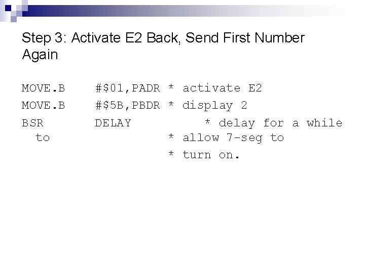
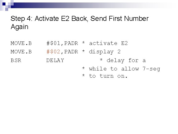
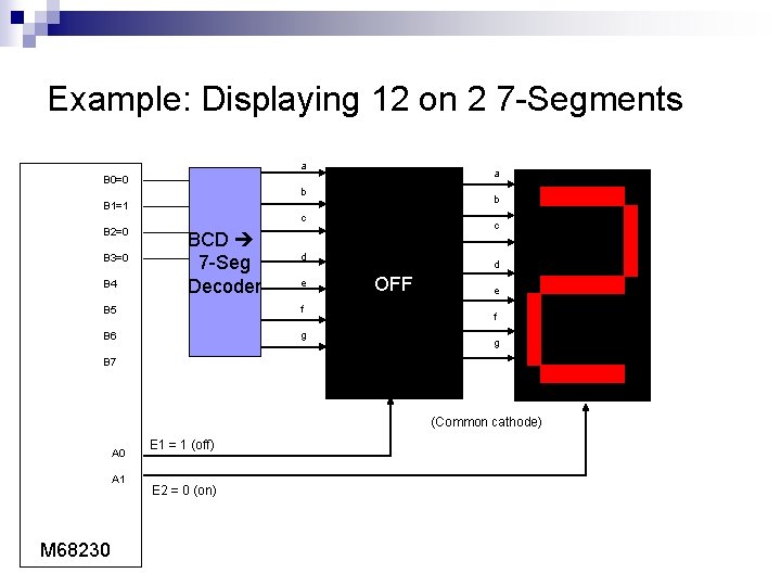
Step 3: Activate E 2 Back, Send First Number Again MOVE. B BSR to #$01, PADR * activate E 2 #$5 B, PBDR * display 2 DELAY * delay for a while * allow 7 -seg to * turn on.

Example: Displaying 12 on 2 7 -Segments B 0=1 B 1=1 B 2=0 B 3=1 B 4=1 a a b b c c d d e B 5=0 B 6=1 OFF e f f g g B 7 (Common cathode) A 0 A 1 M 68230 E 1 = 0 (off) E 2 = 1 (on)

Discussion Using multiplexing, only one digit may be turned on at one time. n But, if the delay is fast enough (<100 ms), our eyes won’t be able to catch the change. n

Example: Displaying 12 on 2 7 -Segments M 68230 a a b b c c B 3 d d B 4 e e B 5 f f B 6 g g B 0 B 1 B 2 B 7 (Common cathode) A 0 A 1 E 2

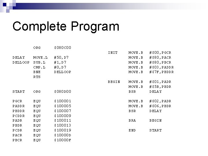
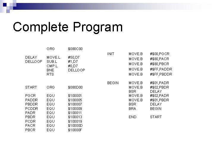
Complete Program ORG DELAY MOVE. L DELLOOP SUB. L CMP. L BNE RTS $080 C 00 INIT MOVE. B #$00, PGCR #$80, PACR #$80, PBCR #$03, PADDR #$7 F, PBDDR BEGIN MOVE. B BSR #$01, PADR #$5 B, PBDR DELAY MOVE. B BSR #$02, PADR #$06, PBDR DELAY BRA BEGIN END START #50, D 7 #1, D 7 #0, D 7 DELLOOP START ORG $080 D 00 PGCR PADDR PBDDR PCDDR PADR PBDR PCDR PACR PBCR EQU EQU EQU $100001 $100005 $100007 $100009 $100011 $100013 $100019 $10000 D $10000 F

Example 2

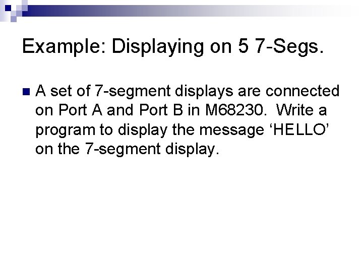
Example: Displaying on 5 7 -Segs. n A set of 7 -segment displays are connected on Port A and Port B in M 68230. Write a program to display the message ‘HELLO’ on the 7 -segment display.

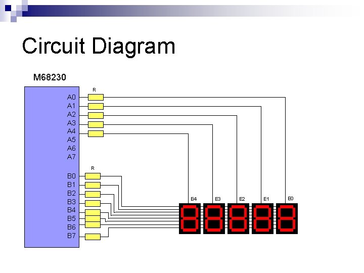
Circuit Diagram M 68230 R A 0 A 1 A 2 A 3 A 4 A 5 A 6 A 7 R B 0 B 1 B 2 B 3 B 4 B 5 B 6 B 7 E 4 E 3 E 2 E 1 E 0

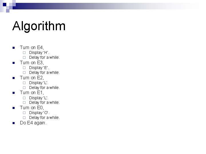
Algorithm n Turn on E 4, ¨ ¨ n Turn on E 3, ¨ ¨ n Display ‘L’. Delay for a while. Turn on E 0, ¨ ¨ n Display ‘L’. Delay for a while. Turn on E 1, ¨ ¨ n Display ‘E’. Delay for a while. Turn on E 2, ¨ ¨ n Display ‘H’. Delay for a while. Display ‘O’. Delay for a while. Do E 4 again.

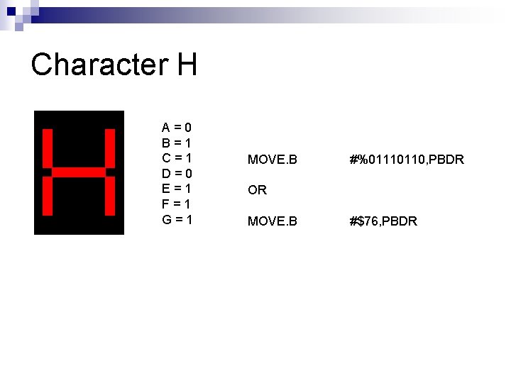
Character H A=0 B=1 C=1 D=0 E=1 F=1 G=1 MOVE. B #%01110110, PBDR OR MOVE. B #$76, PBDR

Character E A=1 B=0 C=0 D=1 E=1 F=1 G=1 MOVE. B #%01111001, PBDR OR MOVE. B #$79, PBDR

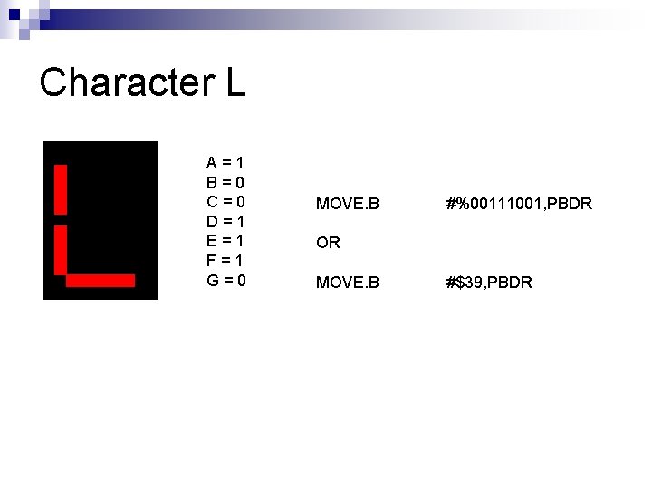
Character L A=1 B=0 C=0 D=1 E=1 F=1 G=0 MOVE. B #%00111001, PBDR OR MOVE. B #$39, PBDR

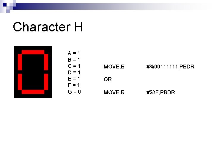
Character H A=1 B=1 C=1 D=1 E=1 F=1 G=0 MOVE. B #%00111111, PBDR OR MOVE. B #$3 F, PBDR

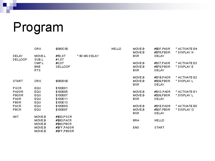
Program ORG $080 C 00 MOVE. L SUB. L CMP. L BNE RTS #50, D 7 #1, D 7 #0, D 7 DELLOOP START ORG $080 D 00 PGCR PADDR PBDDR PADR PBDR PACR PBCR EQU EQU $100001 $100005 $100007 $100011 $100013 $10000 D $10000 F INIT MOVE. B #$00, PGCR #$80, PACR #$80, PBCR #$FF, PADDR #$FF, PBDDR DELAY DELLOOP HELLO * 80 MS DELAY MOVE. B BSR #$0 F, PADR #$76, PBDR DELAY * ACTIVATE E 4 * DISPLAY H MOVE. B BSR #$17, PADR #$79, PBDR DELAY * ACTIVATE E 3 * DISPLAY E MOVE. B BSR #$1 B, PADR #$39, PBDR DELAY * ACTIVATE E 2 * DISPLAY L MOVE. B BSR #$1 D, PADR #$39, PBDR DELAY * ACTIVATE E 1 * DISPLAY L MOVE. B BSR #$1 E, PADR #$3 F, PBDR DELAY * ACTIVATE E 0 * DISPLAY O BRA HELLO END START

7 -Segment + BCD Decoder

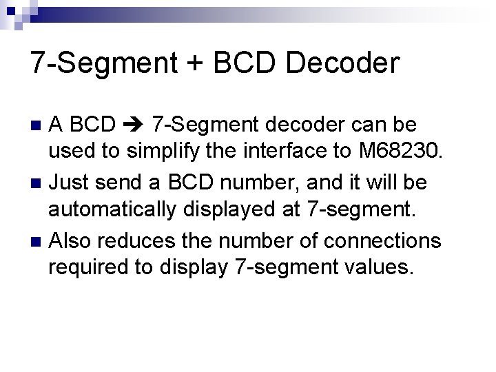
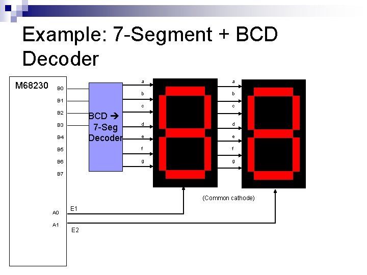
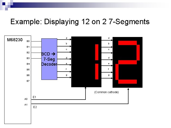
7 -Segment + BCD Decoder A BCD 7 -Segment decoder can be used to simplify the interface to M 68230. n Just send a BCD number, and it will be automatically displayed at 7 -segment. n Also reduces the number of connections required to display 7 -segment values. n

Example: 7 -Segment + BCD Decoder M 68230 a a b b c c d d e e B 5 f f B 6 g g B 0 B 1 B 2 BCD 7 -Seg Decoder B 3 B 4 B 7 (Common cathode) A 0 A 1 E 2

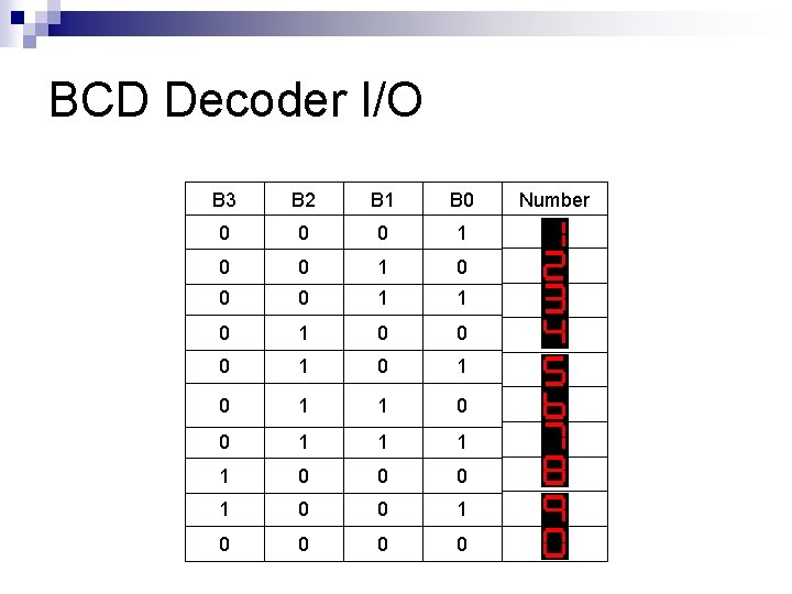
BCD Decoder I/O B 3 B 2 B 1 B 0 Number 0 0 0 1 1 0 0 1 0 2 0 0 1 1 3 0 1 0 0 4 0 1 5 0 1 1 0 6 0 1 1 1 7 1 0 0 0 8 1 0 0 1 9 0 0 0

Example 3

Displaying 12 on 7 -Segments n A circuit is wired as in the next figure. Write a program that displays ‘ 12’ on the 7 -Segment.

Example: 7 -Segment + BCD Decoder M 68230 a a b b c c d d e e B 5 f f B 6 g g B 0 B 1 B 2 BCD 7 -Seg Decoder B 3 B 4 B 7 (Common cathode) A 0 A 1 E 2

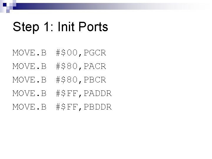
Step 1: Init Ports MOVE. B #$00, PGCR #$80, PACR #$80, PBCR #$FF, PADDR #$FF, PBDDR

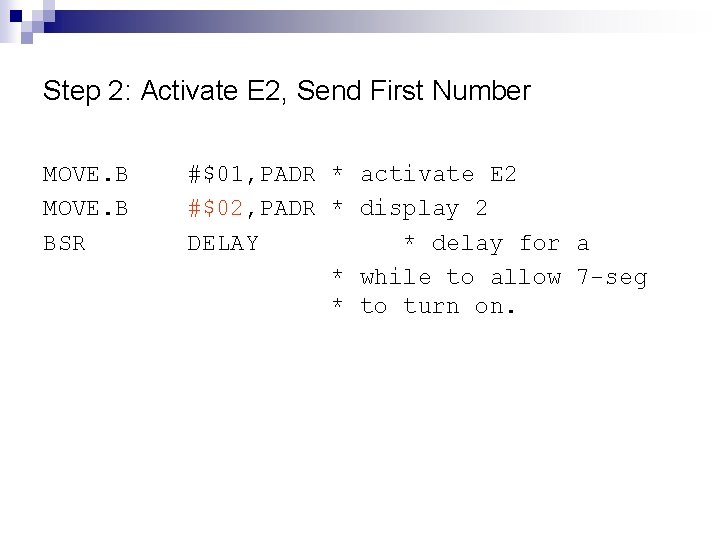
Step 2: Activate E 2, Send First Number MOVE. B BSR #$01, PADR * activate E 2 #$02, PADR * display 2 DELAY * delay for a * while to allow 7 -seg * to turn on.

Example: Displaying 12 on 2 7 -Segments a B 0=0 b B 1=1 B 2=0 B 3=0 B 4 a b c BCD 7 -Seg Decoder c d e B 5 f B 6 g d OFF e f g B 7 (Common cathode) A 0 A 1 M 68230 E 1 = 1 (off) E 2 = 0 (on)

Step 2: Activate E 1, Send Second Number MOVE. B BSR #$02, PADR * activate E 1 #$01, PADR * display 1 DELAY * delay for a while * to allow 7 -seg * to turn on.

Example: Displaying 12 on 2 7 -Segments a B 0=0 b B 1=1 B 2=1 B 3=0 B 4=0 c BCD 7 -Seg Decoder d e B 5=0 f B 6=0 g a b c d e f g B 7 (Common cathode) A 0 A 1 M 68230 E 1 = 0 (on) E 2 = 1 (off) OFF

Step 4: Activate E 2 Back, Send First Number Again MOVE. B BSR #$01, PADR * activate E 2 #$02, PADR * display 2 DELAY * delay for a * while to allow 7 -seg * to turn on.

Example: Displaying 12 on 2 7 -Segments a B 0=0 b B 1=1 B 2=0 B 3=0 B 4 a b c BCD 7 -Seg Decoder c d e B 5 f B 6 g d OFF e f g B 7 (Common cathode) A 0 A 1 M 68230 E 1 = 1 (off) E 2 = 0 (on)

Discussion Using multiplexing, only one digit may be turned on at one time. n But, if the delay is fast enough (<100 ms), our eyes won’t be able to catch the change. n

Example: Displaying 12 on 2 7 -Segments M 68230 a a b b c c d d e e B 5 f f B 6 g g B 0 B 1 B 2 BCD 7 -Seg Decoder B 3 B 4 B 7 (Common cathode) A 0 A 1 E 2

Complete Program ORG $080 C 00 DELAY DELLOOP MOVE. L SUB. L CMP. L BNE RTS #50, D 7 #1, D 7 #0, D 7 DELLOOP START ORG $080 D 00 PGCR PADDR PBDDR PCDDR PADR PBDR PCDR PACR PBCR EQU EQU EQU $100001 $100005 $100007 $100009 $100011 $100013 $100019 $10000 D $10000 F INIT MOVE. B #$00, PGCR #$80, PACR #$80, PBCR #$FF, PADDR #$FF, PBDDR BEGIN MOVE. B BSR BRA #$01, PADR #$02, PBDR DELAY #$02, PADR #$01, PBDR DELAY BEGIN END START

DC Motor

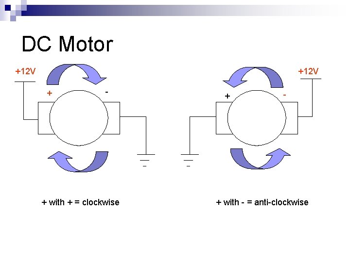
Controlling DC Motors Has two terminals (positive/negative), connected to DC voltage. n If positive voltage applied at positive terminal, motor moves clockwise. n If negative voltage applied at positive terminal, motor moves anti-clockwise. n

DC Motor +12 V + - + with + = clockwise + - + with - = anti-clockwise

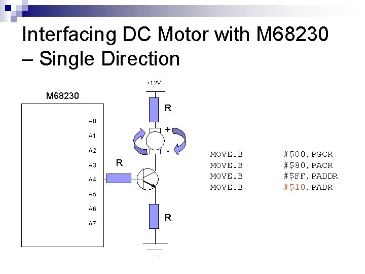
Interfacing DC Motor with M 68230 – Single Direction +12 V M 68230 R A 0 + A 1 - A 2 A 3 R A 4 A 5 A 6 A 7 R MOVE. B #$00, PGCR #$80, PACR #$FF, PADDR #$10, PADR

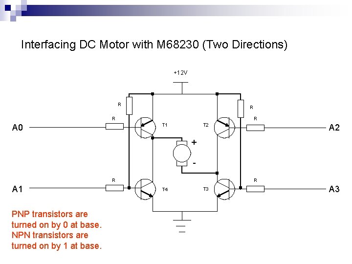
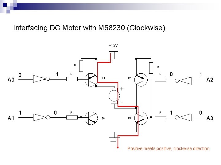
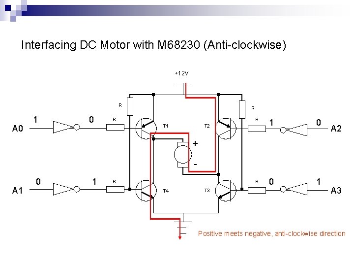
Interfacing DC Motor with M 68230 (Two Directions) +12 V R R T 1 A 0 T 2 A 2 + R A 1 PNP transistors are turned on by 0 at base. NPN transistors are turned on by 1 at base. R T 4 T 3 A 3

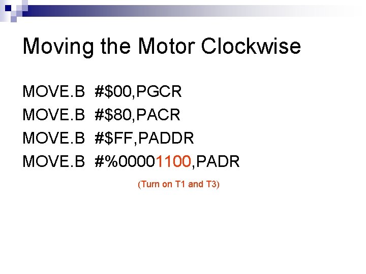
Moving the Motor Clockwise MOVE. B #$00, PGCR #$80, PACR #$FF, PADDR #%00001100, PADR (Turn on T 1 and T 3)

Interfacing DC Motor with M 68230 (Clockwise) +12 V R A 0 0 1 R R R T 1 T 2 0 1 1 0 A 2 + A 1 1 0 R R T 4 T 3 A 3 Positive meets positive, clockwise direction

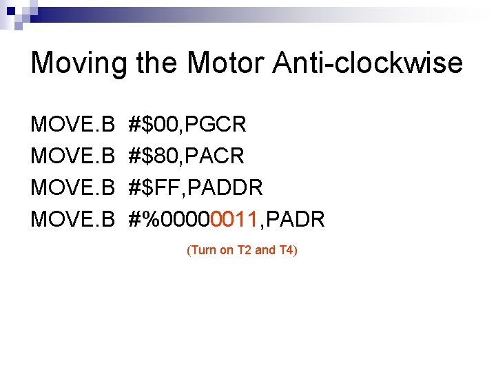
Moving the Motor Anti-clockwise MOVE. B #$00, PGCR #$80, PACR #$FF, PADDR #%00000011, PADR (Turn on T 2 and T 4)

Interfacing DC Motor with M 68230 (Anti-clockwise) +12 V R A 0 1 0 R R R T 1 T 2 1 0 0 1 A 2 + A 1 0 1 R R T 4 T 3 A 3 Positive meets negative, anti-clockwise direction

Keypad

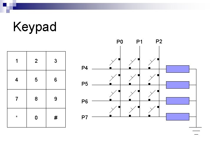
Keypad A set of switches. n CPU determines what button pressed by scanning each column in turn. n Need to be de-bounced after each key press: n ¨ Done using de-bouncing subroutine.

Keypad P 0 1 2 3 P 4 4 5 6 7 8 9 * 0 # P 5 P 6 P 7 P 1 P 2

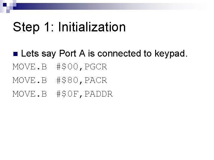
Step 1: Initialization Lets say Port A is connected to keypad. MOVE. B #$00, PGCR MOVE. B #$80, PACR MOVE. B #$0 F, PADDR n

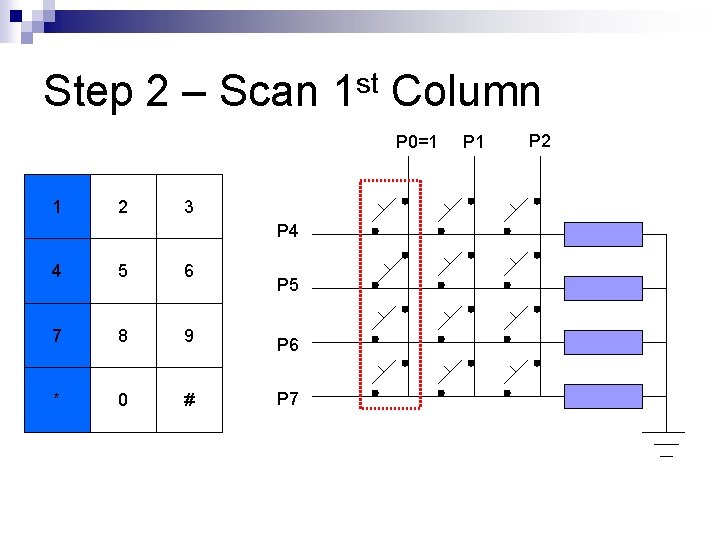
Step 2 – Scan 1 st Column P 0=1 1 2 3 P 4 4 5 6 7 8 9 * 0 # P 5 P 6 P 7 P 1 P 2

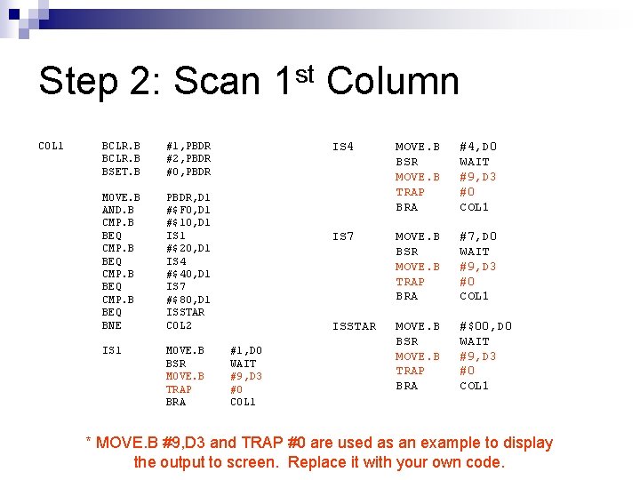
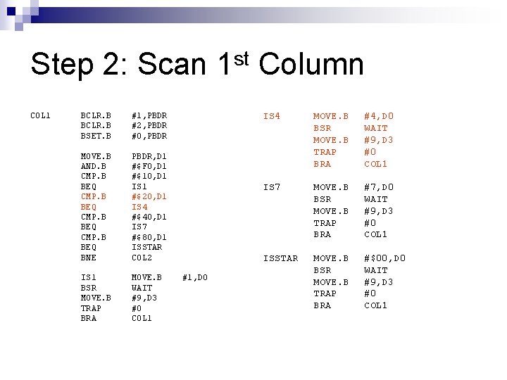
Step 2: Scan 1 st Column COL 1 BCLR. B BSET. B #1, PBDR #2, PBDR #0, PBDR MOVE. B AND. B CMP. B BEQ BNE PBDR, D 1 #$F 0, D 1 #$10, D 1 IS 1 #$20, D 1 IS 4 #$40, D 1 IS 7 #$80, D 1 ISSTAR COL 2 IS 1 MOVE. B BSR MOVE. B TRAP BRA #1, D 0 WAIT #9, D 3 #0 COL 1 IS 4 MOVE. B BSR MOVE. B TRAP BRA #4, D 0 WAIT #9, D 3 #0 COL 1 IS 7 MOVE. B BSR MOVE. B TRAP BRA #7, D 0 WAIT #9, D 3 #0 COL 1 ISSTAR MOVE. B BSR MOVE. B TRAP BRA #$00, D 0 WAIT #9, D 3 #0 COL 1 * MOVE. B #9, D 3 and TRAP #0 are used as an example to display the output to screen. Replace it with your own code.

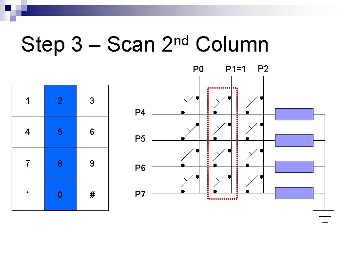
Step 3 – Scan 2 nd Column P 0 1 2 3 P 4 4 5 6 7 8 9 * 0 # P 5 P 6 P 7 P 1=1 P 2

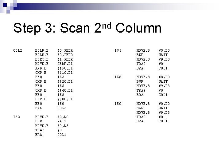
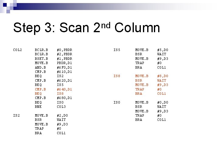
Step 3: Scan 2 nd Column COL 2 IS 2 BCLR. B BSET. B MOVE. B AND. B CMP. B BEQ BNE #0, PBDR #2, PBDR #1, PBDR, D 1 #$F 0, D 1 #$10, D 1 IS 2 #$20, D 1 IS 5 #$40, D 1 IS 8 #$80, D 1 IS 0 COL 3 MOVE. B BSR MOVE. B TRAP BRA #2, D 0 WAIT #9, D 3 #0 COL 1 IS 5 MOVE. B BSR MOVE. B TRAP BRA #5, D 0 WAIT #9, D 3 #0 COL 1 IS 8 MOVE. B BSR MOVE. B TRAP BRA #8, D 0 WAIT #9, D 3 #0 COL 1 IS 0 MOVE. B BSR MOVE. B TRAP BRA #0, D 0 WAIT #9, D 3 #0 COL 1

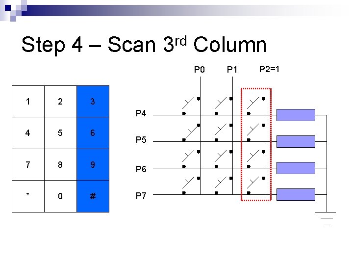
Step 4 – Scan 3 rd Column P 0 1 2 3 P 4 4 5 6 7 8 9 * 0 # P 5 P 6 P 7 P 1 P 2=1

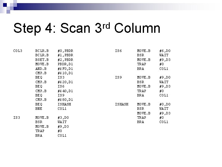
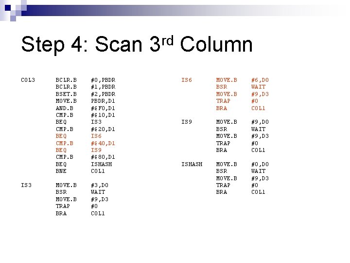
Step 4: Scan 3 rd Column COL 3 IS 3 BCLR. B BSET. B MOVE. B AND. B CMP. B BEQ BNE #0, PBDR #1, PBDR #2, PBDR, D 1 #$F 0, D 1 #$10, D 1 IS 3 #$20, D 1 IS 6 #$40, D 1 IS 9 #$80, D 1 ISHASH COL 1 MOVE. B BSR MOVE. B TRAP BRA #3, D 0 WAIT #9, D 3 #0 COL 1 IS 6 MOVE. B BSR MOVE. B TRAP BRA #6, D 0 WAIT #9, D 3 #0 COL 1 IS 9 MOVE. B BSR MOVE. B TRAP BRA #9, D 0 WAIT #9, D 3 #0 COL 1 ISHASH MOVE. B BSR MOVE. B TRAP BRA #0, D 0 WAIT #9, D 3 #0 COL 1

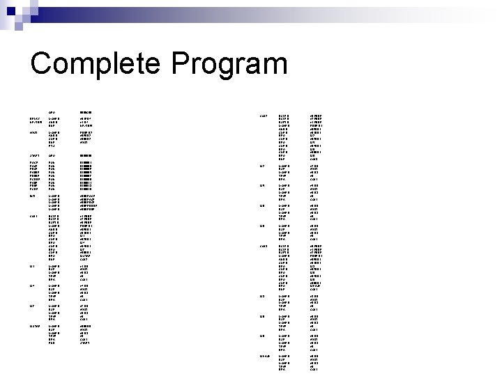
Complete Program ORG $080 C 00 DELAY NEXTDEL MOVE. B SUB. B BNE #$1 F, D 4 #1, D 4 NEXTDEL WAIT MOVE. B AND. B CMP. B BNE RTS PBDR, D 2 #$F 0, D 2 #$00, D 2 WAIT START ORG $080 D 00 PGCR PACR PBCR PADDR PBDDR PCDDR PADR PBDR PCDR EQU EQU EQU $100001 $10000 D $10000 F $100005 $100007 $100009 $100011 $100013 $100019 INIT MOVE. B #$00, PGCR #$80, PACR #$80, PBCR #$0 F, PBDDR #$00, PBDR COL 1 BCLR. B BSET. B MOVE. B AND. B CMP. B BEQ BNE #1, PBDR #2, PBDR #0, PBDR, D 1 #$F 0, D 1 #$10, D 1 IS 1 #$20, D 1 IS 4 #$40, D 1 IS 7 #$80, D 1 ISSTAR COL 2 IS 1 MOVE. B BSR MOVE. B TRAP BRA #1, D 0 WAIT #9, D 3 #0 COL 1 IS 4 MOVE. B BSR MOVE. B TRAP BRA #4, D 0 WAIT #9, D 3 #0 COL 1 MOVE. B BSR MOVE. B TRAP BRA #7, D 0 WAIT #9, D 3 #0 COL 1 MOVE. B BSR MOVE. B TRAP BRA END #$00, D 0 WAIT #9, D 3 #0 COL 1 START IS 7 ISSTAR COL 2 BCLR. B BSET. B MOVE. B AND. B CMP. B BEQ BNE #0, PBDR #2, PBDR #1, PBDR, D 1 #$F 0, D 1 #$10, D 1 IS 2 #$20, D 1 IS 5 #$40, D 1 IS 8 #$80, D 1 IS 0 COL 3 IS 2 MOVE. B BSR MOVE. B TRAP BRA #2, D 0 WAIT #9, D 3 #0 COL 1 IS 5 MOVE. B BSR MOVE. B TRAP BRA #5, D 0 WAIT #9, D 3 #0 COL 1 IS 8 MOVE. B BSR MOVE. B TRAP BRA #8, D 0 WAIT #9, D 3 #0 COL 1 IS 0 MOVE. B BSR MOVE. B TRAP BRA #0, D 0 WAIT #9, D 3 #0 COL 1 COL 3 BCLR. B BSET. B MOVE. B AND. B CMP. B BEQ BNE #0, PBDR #1, PBDR #2, PBDR, D 1 #$F 0, D 1 #$10, D 1 IS 3 #$20, D 1 IS 6 #$40, D 1 IS 9 #$80, D 1 ISHASH COL 1 IS 3 MOVE. B BSR MOVE. B TRAP BRA #3, D 0 WAIT #9, D 3 #0 COL 1 IS 6 MOVE. B BSR MOVE. B TRAP BRA #6, D 0 WAIT #9, D 3 #0 COL 1 IS 9 MOVE. B BSR MOVE. B TRAP BRA #9, D 0 WAIT #9, D 3 #0 COL 1 ISHASH MOVE. B BSR MOVE. B TRAP BRA #0, D 0 WAIT #9, D 3 #0 COL 1

Example

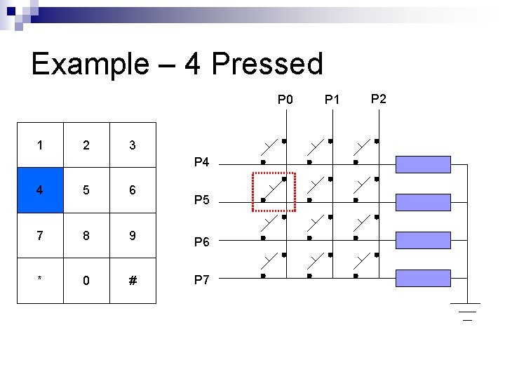
Example – 4 Pressed P 0 1 2 3 P 4 4 5 6 7 8 9 * 0 # P 5 P 6 P 7 P 1 P 2

Step 2: Scan 1 st Column COL 1 BCLR. B BSET. B #1, PBDR #2, PBDR #0, PBDR MOVE. B AND. B CMP. B BEQ BNE PBDR, D 1 #$F 0, D 1 #$10, D 1 IS 1 #$20, D 1 IS 4 #$40, D 1 IS 7 #$80, D 1 ISSTAR COL 2 IS 1 BSR MOVE. B TRAP BRA MOVE. B WAIT #9, D 3 #0 COL 1 #1, D 0 IS 4 MOVE. B BSR MOVE. B TRAP BRA #4, D 0 WAIT #9, D 3 #0 COL 1 IS 7 MOVE. B BSR MOVE. B TRAP BRA #7, D 0 WAIT #9, D 3 #0 COL 1 ISSTAR MOVE. B BSR MOVE. B TRAP BRA #$00, D 0 WAIT #9, D 3 #0 COL 1

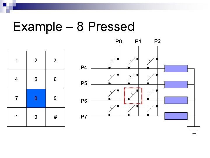
Example – 8 Pressed P 0 1 2 3 P 4 4 5 6 7 8 9 * 0 # P 5 P 6 P 7 P 1 P 2

Step 3: Scan 2 nd Column COL 2 IS 2 BCLR. B BSET. B MOVE. B AND. B CMP. B BEQ BNE #0, PBDR #2, PBDR #1, PBDR, D 1 #$F 0, D 1 #$10, D 1 IS 2 #$20, D 1 IS 5 #$40, D 1 IS 8 #$80, D 1 IS 0 COL 3 MOVE. B BSR MOVE. B TRAP BRA #2, D 0 WAIT #9, D 3 #0 COL 1 IS 5 MOVE. B BSR MOVE. B TRAP BRA #5, D 0 WAIT #9, D 3 #0 COL 1 IS 8 MOVE. B BSR MOVE. B TRAP BRA #8, D 0 WAIT #9, D 3 #0 COL 1 IS 0 MOVE. B BSR MOVE. B TRAP BRA #0, D 0 WAIT #9, D 3 #0 COL 1

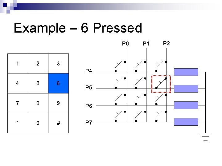
Example – 6 Pressed P 0 1 2 3 P 4 4 5 6 7 8 9 * 0 # P 5 P 6 P 7 P 1 P 2

Step 4: Scan 3 rd Column COL 3 IS 3 BCLR. B BSET. B MOVE. B AND. B CMP. B BEQ BNE #0, PBDR #1, PBDR #2, PBDR, D 1 #$F 0, D 1 #$10, D 1 IS 3 #$20, D 1 IS 6 #$40, D 1 IS 9 #$80, D 1 ISHASH COL 1 MOVE. B BSR MOVE. B TRAP BRA #3, D 0 WAIT #9, D 3 #0 COL 1 IS 6 MOVE. B BSR MOVE. B TRAP BRA #6, D 0 WAIT #9, D 3 #0 COL 1 IS 9 MOVE. B BSR MOVE. B TRAP BRA #9, D 0 WAIT #9, D 3 #0 COL 1 ISHASH MOVE. B BSR MOVE. B TRAP BRA #0, D 0 WAIT #9, D 3 #0 COL 1

Delay Subroutine

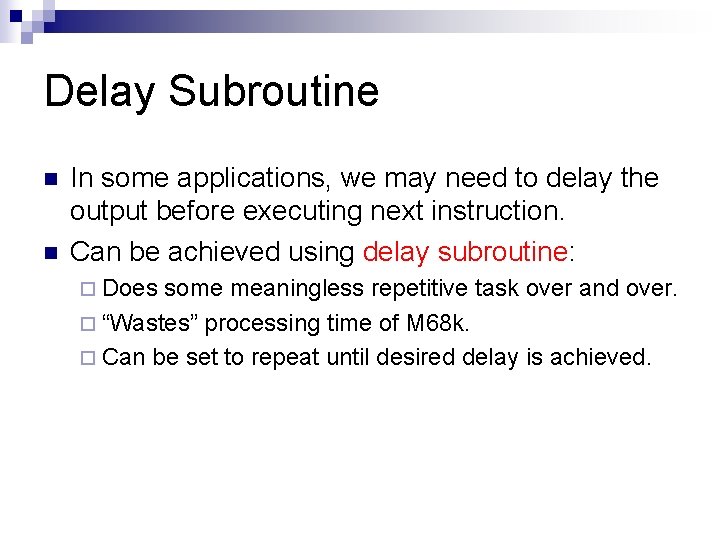
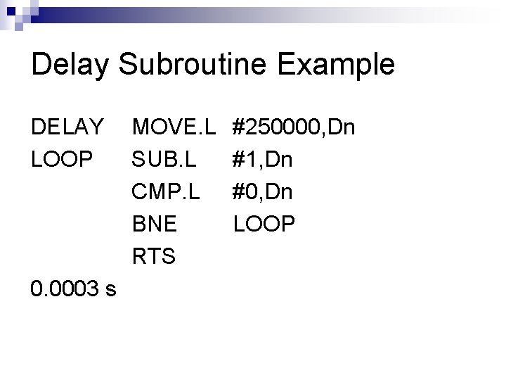
Delay Subroutine n n In some applications, we may need to delay the output before executing next instruction. Can be achieved using delay subroutine: ¨ Does some meaningless repetitive task over and over. ¨ “Wastes” processing time of M 68 k. ¨ Can be set to repeat until desired delay is achieved.

Delay Subroutine Example DELAY LOOP 0. 0003 s MOVE. L SUB. L CMP. L BNE RTS #250000, Dn #1, Dn #0, Dn LOOP

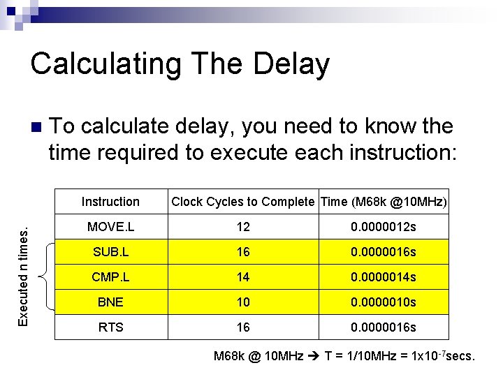
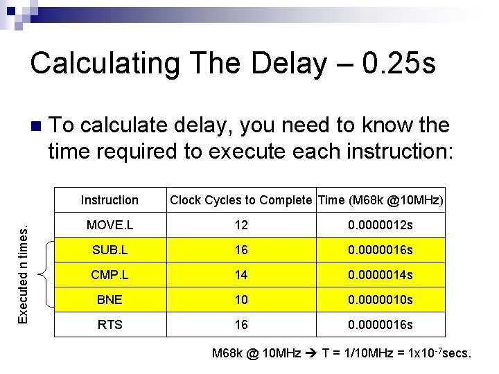
Calculating The Delay n To calculate delay, you need to know the time required to execute each instruction: Executed n times. Instruction Clock Cycles to Complete Time (M 68 k @10 MHz) MOVE. L 12 0. 0000012 s SUB. L 16 0. 0000016 s CMP. L 14 0. 0000014 s BNE 10 0. 0000010 s RTS 16 0. 0000016 s M 68 k @ 10 MHz T = 1/10 MHz = 1 x 10 -7 secs.

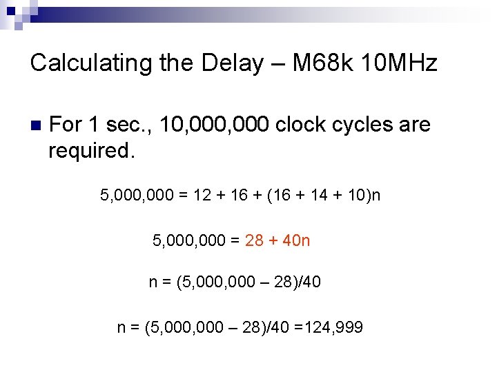
Calculating the Delay – M 68 k 10 MHz n For 1 sec. , 10, 000 clock cycles are required. 5, 000 = 12 + 16 + (16 + 14 + 10)n 5, 000 = 28 + 40 n n = (5, 000, 000 – 28)/40 =124, 999

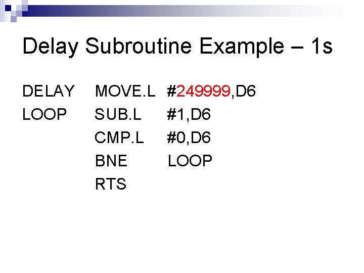
Delay Subroutine Example – 1 s DELAY LOOP MOVE. L SUB. L CMP. L BNE RTS #249999, D 6 #1, D 6 #0, D 6 LOOP

Calculating The Delay – 0. 25 s n To calculate delay, you need to know the time required to execute each instruction: Executed n times. Instruction Clock Cycles to Complete Time (M 68 k @10 MHz) MOVE. L 12 0. 0000012 s SUB. L 16 0. 0000016 s CMP. L 14 0. 0000014 s BNE 10 0. 0000010 s RTS 16 0. 0000016 s M 68 k @ 10 MHz T = 1/10 MHz = 1 x 10 -7 secs.

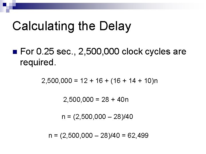
Calculating the Delay n For 0. 25 sec. , 2, 500, 000 clock cycles are required. 2, 500, 000 = 12 + 16 + (16 + 14 + 10)n 2, 500, 000 = 28 + 40 n n = (2, 500, 000 – 28)/40 = 62, 499

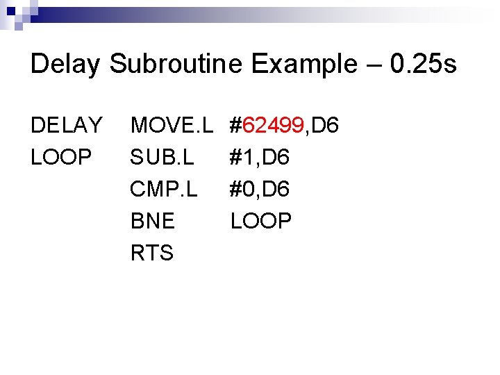
Delay Subroutine Example – 0. 25 s DELAY LOOP MOVE. L SUB. L CMP. L BNE RTS #62499, D 6 #1, D 6 #0, D 6 LOOP

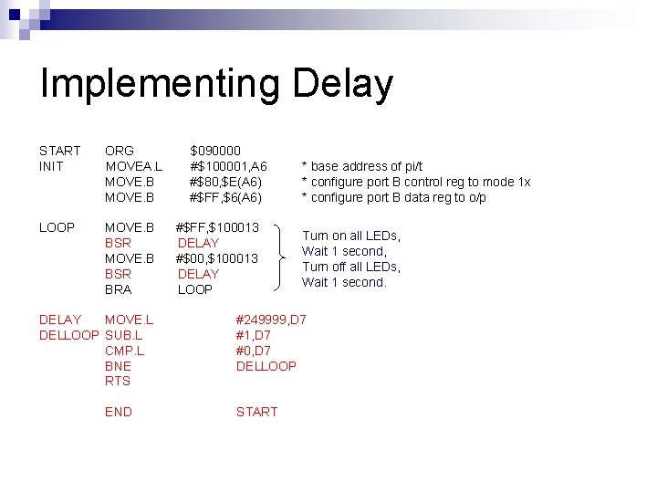
Implementing Delay START INIT ORG MOVEA. L MOVE. B LOOP MOVE. B BSR BRA DELAY MOVE. L DELLOOP SUB. L CMP. L BNE RTS END $090000 #$100001, A 6 #$80, $E(A 6) #$FF, $6(A 6) #$FF, $100013 DELAY #$00, $100013 DELAY LOOP * base address of pi/t * configure port B control reg to mode 1 x * configure port B data reg to o/p Turn on all LEDs, Wait 1 second, Turn off all LEDs, Wait 1 second. #249999, D 7 #1, D 7 #0, D 7 DELLOOP START

Conclusion

Conclusion The M 68230 is a parallel interface used by M 68 k to connect with various devices. n The M 68230 has three ports, which can be configured to interface with many devices. n To use the ports, it MUST be initialized first. n

Conclusion The delay subroutine is used to “waste” the CPU’s time by telling it to do repetitive tasks. n The delay format is basically the same, just adjust the counter to get the delay you want. n

The End Please read: Antonakos, pg. 352 -366 M 68230 Datasheet Ablelogic, Abitec, VTES Manuals