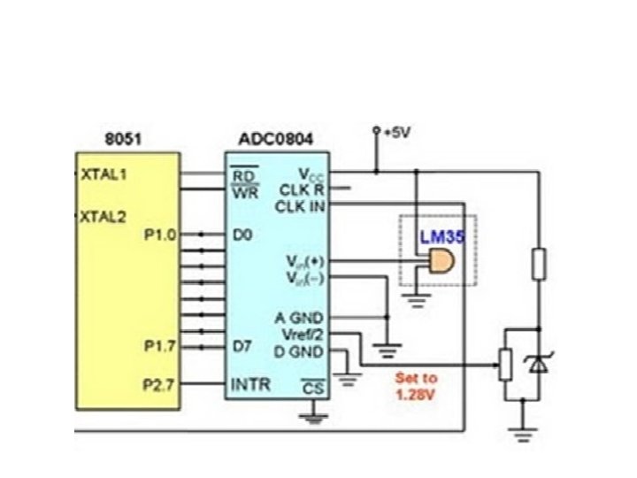
Interfacing ADC to 8051 ADC 0804 is an


- Slides: 12

Interfacing ADC to 8051

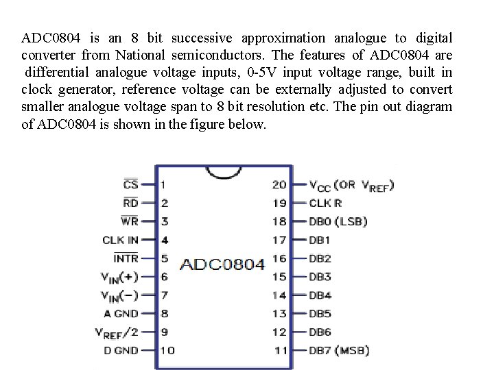
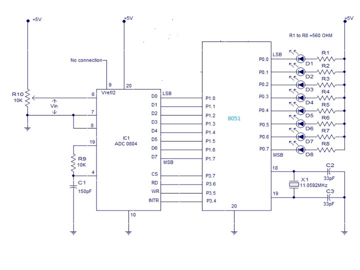
ADC 0804 is an 8 bit successive approximation analogue to digital converter from National semiconductors. The features of ADC 0804 are differential analogue voltage inputs, 0 -5 V input voltage range, built in clock generator, reference voltage can be externally adjusted to convert smaller analogue voltage span to 8 bit resolution etc. The pin out diagram of ADC 0804 is shown in the figure below.

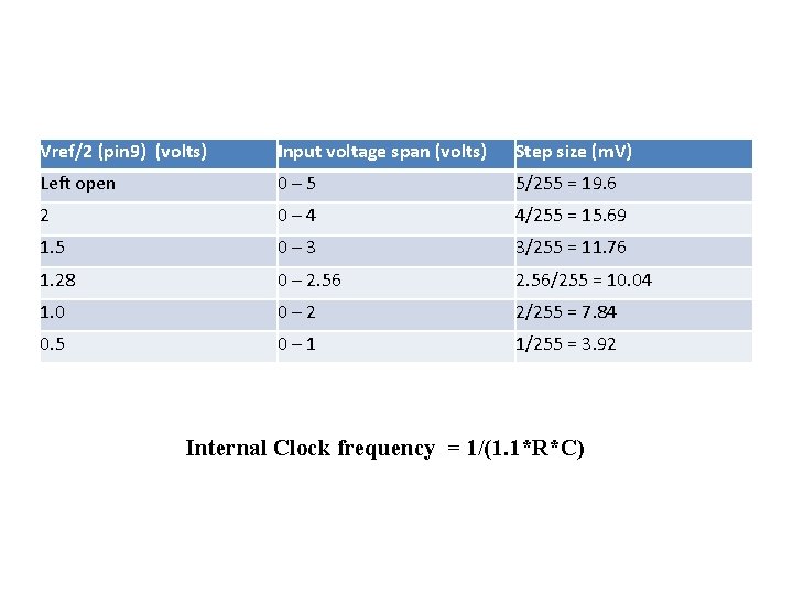
Vref/2 (pin 9) (volts) Input voltage span (volts) Step size (m. V) Left open 0– 5 5/255 = 19. 6 2 0– 4 4/255 = 15. 69 1. 5 0– 3 3/255 = 11. 76 1. 28 0 – 2. 56/255 = 10. 04 1. 0 0– 2 2/255 = 7. 84 0. 5 0– 1 1/255 = 3. 92 Internal Clock frequency = 1/(1. 1*R*C)

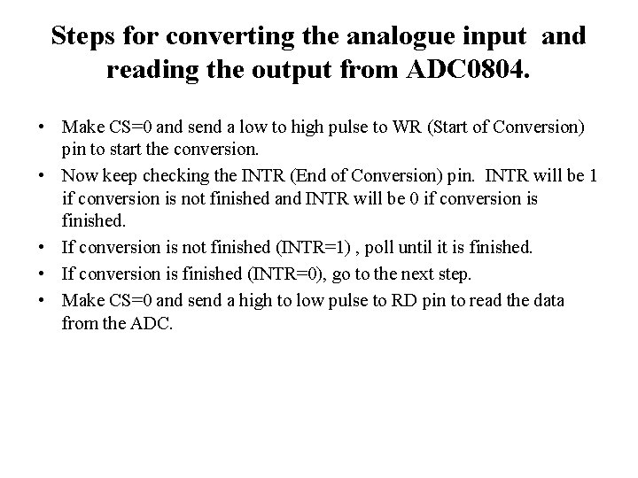
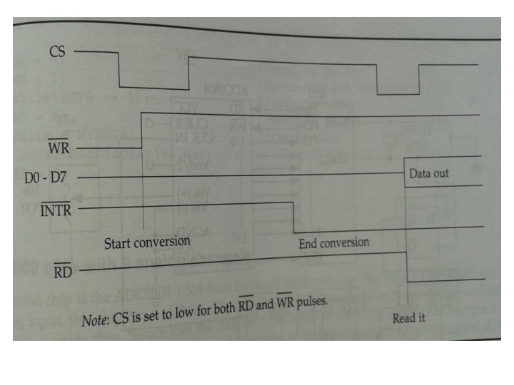
Steps for converting the analogue input and reading the output from ADC 0804. • Make CS=0 and send a low to high pulse to WR (Start of Conversion) pin to start the conversion. • Now keep checking the INTR (End of Conversion) pin. INTR will be 1 if conversion is not finished and INTR will be 0 if conversion is finished. • If conversion is not finished (INTR=1) , poll until it is finished. • If conversion is finished (INTR=0), go to the next step. • Make CS=0 and send a high to low pulse to RD pin to read the data from the ADC.


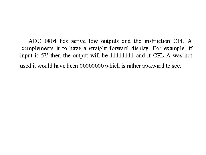
ADC 0804 has active low outputs and the instruction CPL A complements it to have a straight forward display. For example, if input is 5 V then the output will be 1111 and if CPL A was not used it would have been 0000 which is rather awkward to see.

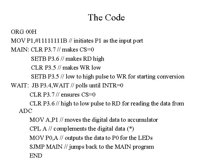
The Code ORG 00 H MOV P 1, #1111 B // initiates P 1 as the input port MAIN: CLR P 3. 7 // makes CS=0 SETB P 3. 6 // makes RD high CLR P 3. 5 // makes WR low SETB P 3. 5 // low to high pulse to WR for starting conversion WAIT: JB P 3. 4, WAIT // polls until INTR=0 CLR P 3. 7 // ensures CS=0 CLR P 3. 6 // high to low pulse to RD for reading the data from ADC MOV A, P 1 // moves the digital data to accumulator CPL A // complements the digital data (*) MOV P 0, A // outputs the data to P 0 for the LEDs SJMP MAIN // jumps back to the MAIN program END

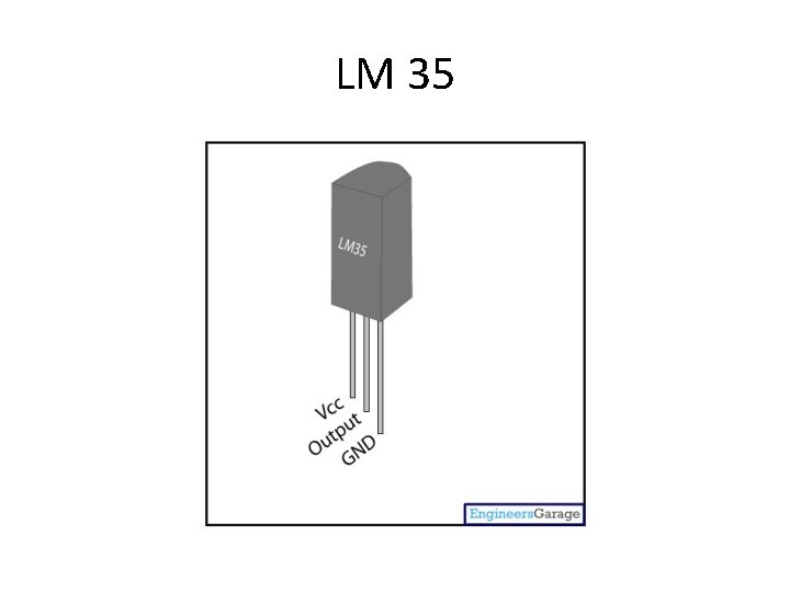
LM 35

Thermistor vs LM 35 • Linear • -55 C to 150 C • Low self heating 0. 1 C

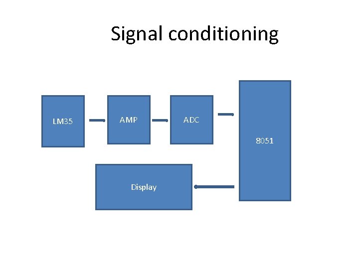
Signal conditioning LM 35 AMP ADC 8051 Display
