UNIT3 IO INTERFACING Presented by R BENSCHWARTZ 1

UNIT-3 I/O INTERFACING Presented by R. BENSCHWARTZ 1

UNIT 3 Syllabus • • • Memory Interfacing & I/O interfacing Parallel communication interface {8255 PPI} Serial communication interface {8251 USART} D/A and A/D Interface {ADC 0800/0809, DAC 0800} Timer {or counter} – {8253/8254 Timer} Keyboard /display controller {8279} Interrupt controller {8259} DMA controller {8237/8257} Programming and applications Case studies 1. Traffic Light control 2. LED display 3. LCD display 4. Keyboard display interface 5. Alarm Controller 2

Data Transfers Synchronous ----- Usually occur when peripherals are located within the same computer as the CPU. Close proximity allows all state bits change at same time on a common clock. Asynchronous ----- Do not require that the source and destination use the same system clock. 3

4 Memory & IO Interfacing MEMORY DEVICES I/O DEVICES Presented by C. GOKUL, AP/EEE , Velalar College of Engg & Tech, Erode
 or I/O devices to 8086")
5 interface memory (RAM, ROM, EPROM'. . . ) or I/O devices to 8086 microprocessor. Several memory chips or I/O devices can connected to a microprocessor. An address decoding circuit is used to select the required I/O device or a memory chip.

IO mapped IO V/s Memory Mapped IO Mapped IO IO is treated as memory. 16 -bit addressing. More Decoder Hardware. Can address 216=64 k locations. Less memory is available. IO is treated IO. 8 - bit addressing. Less Decoder Hardware. Can address 28=256 locations. Whole memory address space is available. 6

7 Memory Mapped IO IO Mapped IO • Memory Instructions are • used. • Memory control signals • are used. • Arithmetic and logic • operations can be performed on data. • Data transfer b/w • register and IO. Special Instructions are used like IN, OUT. Special control signals are used. Arithmetic and logic operations can not be performed on data. Data transfer b/w accumulator and IO.

8 Parallel communication interface INTEL 8255 Presented by C. GOKUL, AP/EEE , Velalar College of Engg & Tech, Erode

9 8255 PPI • • The 8255 chip is also called as Programmable Peripheral Interface. The Intel’s 8255 is designed for use with Intel’s 8 bit, 16 -bit and higher capability microprocessors The 8255 is a 40 pin integrated circuit (IC), designed to perform a variety of interface functions in a computer environment. It is flexible and economical.

PIN DIAGRAM OF 8255 10

Signals of 8085 11

8255 PIO/PPI It has 24 input/output lines which may be individually programmed. 2 groups of I/O pins are named as Group A (Port-A & Port C Upper) Group B (Port-B & Port C Lower) 3 ports(each port has 8 bit) Port A lines are identified by symbols PA 0 -PA 7 Port B lines are identified by symbols PB 0 -PB 7 Port C lines are identified by PC 0 -PC 7 , PC 3 -PC 0 ie: PORT C UPPER(PC 7 -PC 4) , PORT C LOWER(PC 3 -PC 0) 12

D 0 - D 7: data input/output lines for the device. All information read from and written to the 8255 occurs via these 8 data lines. CS (Chip Select). If this line is a logical 0, the microprocessor can read and write to the 8255. RESET : The 8255 is placed into its reset state if this input line is a logical 1 13

14 • • • RD : This is the input line driven by the microprocessor and should be low to indicate read operation to 8255. WR : This is an input line driven by the microprocessor. A low on this line indicates write operation. A 1 -A 0 : These are the address input lines and are driven by the microprocessor.

15 Control Logic CS signal is the master Chip Select A 0 and A 1 specify one of the two I/O Ports CS A 1 A 0 0 0 0 1 1 X X Selected Port A Port B Port C Control Register 8255 is not selected

Block Diagram of 8255 A 16
 It has a 40 pins of 4 parts. 1.")
Block Diagram of 8255 (Architecture) It has a 40 pins of 4 parts. 1. Data bus buffer 2. Read/Write control logic 3. Group A and Group B controls 4. Port A, B and C 17

18 1. Data bus buffer This is a tristate bidirectional buffer used to interface the 8255 to system data bus. Data is transmitted or received by the buffer on execution of input or output instruction by the CPU.
")
19 2. Read/Write control logic This unit accepts control signals ( RD, WR ) and also inputs from address bus and issues commands to individual group of control blocks ( Group A, Group B). It has the following pins. CS , RD , WR , RESET , A 1 , A 0

20 3. Group A and Group B controls These block receive control from the CPU and issues commands to their respective ports. Group A - PA and PCU ( PC 7 –PC 4) Group B – PB and PCL ( PC 3 –PC 0) a) Port A: This has an 8 bit latched/buffered O/P and 8 bit input latch. It can be programmed in 3 modes – mode 0, mode 1, mode 2. •
 Port B: It can be programmed in mode 0, mode 1 c)")
21 b) Port B: It can be programmed in mode 0, mode 1 c) Port C : It can be programmed in mode 0
")
22 CONTROL WORD REGISTER(CWR)
 Mode Set/Reset bits in Port C")
23 Modes of Operation of 8255 Bit Set/Reset(BSR) Mode Set/Reset bits in Port C I/O Mode 0 (Simple input/output) Mode 1 (Handshake mode) Mode 2 (Bidirectional Data Transfer)

1. BSR Mode 24

B 3 B 2 B 1 0 0 1 1 0 1 0 1 Bit/pin of port C selected Concerned only with the 8 -bits of Port C. Set or Reset by control word Ports A and B are not affected PC 0 PC 1 PC 2 PC 3 PC 4 PC 5 PC 6 PC 7 25
 Mode 0 (Simple Input or Output): • Ports A and")
2. I/O MODE a) Mode 0 (Simple Input or Output): • Ports A and B are used as Simple I/O Ports Port C as two 4 -bit ports • Features • Outputs are latched – Inputs are not latched – Ports do not have handshake or interrupt capability – 26

27
 Mode 1: (Input or Output with Handshake) • Handshake signals are exchanged between")
b) Mode 1: (Input or Output with Handshake) • Handshake signals are exchanged between MPU & Peripherals • Features – – Ports A and B are used as Simple I/O Ports Each port uses 3 lines from Port C as handshake signals Input & Output data are latched interrupt logic supported 28
 Mode 2: Bidirectional Data Transfer • • Used primarily in applications such")
29 c) Mode 2: Bidirectional Data Transfer • • Used primarily in applications such as data transfer between two computers Features – – Ports A can be configured as the bidirectional Port B in Mode 0 or Mode 1. Port A uses 5 Signals from Port C as handshake signals for data transfer Remaining 3 Signals from Port C Used as – Simple I/O or handshake for Port B
 Port A: output with handshake (2) Port B: input")
30 Find control word (1) Port A: output with handshake (2) Port B: input with handshake (3) Port CL: output (4)Port CU: input Solution: 1 0 1 1 1 0 = AEH

31 Port A: Output, Port B: Output, Port CU: Output, Port CL: Output Solution: 1 0 0 0 0 = 80 H The control word register for the above ports of Intel 8255 is 80 H.

32 Port A: Input, Port B: Input, Port CU: Input, Port CL: Input Solution: 1 0 0 1 1 = 9 BH The control word register for the above ports of intel 8255 is 9 BH.

Basics of serial communication 1. Transmitter: - A parallel-in, serial-out shift register Receiver: - A serial-in, parallel-out shift register. 2. - 33 Parallel Transfer

TRANSMITTER Receiver 34

Serial communication interface INTEL 8251 USART 35
 Programmable chip designed for synchronous and asynchronous serial")
UNIVERSAL SYNCHRONOUS ASYNCHRONOUS RECEIVER TRANSMITTER (USART) Programmable chip designed for synchronous and asynchronous serial data transmission 28 pin DIP Coverts the parallel data into a serial stream of bits suitable for serial transmission. Receives a serial stream of bits and convert it into parallel data bytes to be 36

37

BLOCK DIAGRAM 38

Five Sections – – – Read/Write Control Logic • Interfaces the chip with MPU • Determine the functions according to the control word • Monitors data flow Transmitter • Converts parallel word received from MPU into serial bits • Transmits serial bits over TXD line to a peripheral. Receiver • Receives serial bits from peripheral • Converts serial bits into parallel word • Transfers the parallel word to the MPU Data Bus Buffer- 8 bit Bidirectional bus. Modem Controller • Used to establish data communication modems over telephone line 39

Input Signals CS – Chip Select When this signal goes low, 8251 is selected by MPU for communication C/D – Control/Data When this signal is high, the control register or status register is addressed When it is low, the data buffer is addressed Control and Status register is differentiated by WR and RD signals, respectively 40

41 • WR – Write – – • RD – Read – – • • writes in the control register or sends outputs to the data buffer. This connected to IOW or MEMW Either reads a status from status register or accepts data from the data buffer This is connected to either IOR or MEMR RESET - Reset CLK - Clock – – Connected to system clock Necessary for communication with microprocessor.

42 CS C/D RD WR Function 0 1 1 0 MPU writes instruction in the control register 0 1 MPU reads status from the status register 0 0 1 0 MPU outputs the data to the Data Buffer 0 0 0 1 MPU accepts data from the Data Buffer 1 X X X USART is not Selected

43 • Control Register – 16 -bit register – This register can be accessed an output port when the C/D pin is high • Status Register – Checks ready status of a peripheral • Data Buffer

Transmitter Section Accepts parallel data and converts it into serial data Two registers Buffer Register Y Output Register Y To hold eight bits Converts eight bits into a stream of serial bits Transmits data on Tx. D pin with appropriate framing bits(Start and Stop) 44

Signals Associated with Transmitter Section • • Tx. D – Transmit Data – Serial bits are transmitted on this line Tx. C – Transmitter Clock – Controls the rate at which bits are transmitted Tx. RDY – Transmitter Ready – Can be used either to interrupt the MPU or indicate the status Tx. E – Transmitter Empty – Logic 1 on this line indicate that the output register is empty 45

Receiver Section Accepts serial data from peripheral and converts it into parallel data The section has two registers Input Register Buffer Register 46

Signals Associated with Receiver Section Rx. D – Receive Data Bits are received serially on this line and converted into parallel byte in the receiver input Rx. C – Receiver Clock Rx. RDY – Receiver Ready It goes high when the USART has a character in the buffer register and is ready to transfer it to the MPU 47

Signals Associated with Modem Control • DSR- Data Set Ready – • DTR – Data Terminal Ready – • device is ready to accept data when the 8251 is communicating with a modem. RTS – Request to send Data – • Normally used to check if the Data Set is ready when communicating with a modem the receiver is ready to receive a data byte from modem CTS – Clear to Send 48

49 Control words

50

51

52

53
 with 8085 processor: 54")
Interfacing of 8255(PPI) with 8085 processor: 54

55

11 -56 Programming 8251 q 8251 mode register 7 6 5 Number of Stop bits 00: invalid 01: 1 bit 10: 1. 5 bits 11: 2 bits 4 3 2 1 0 Mode register Baud Rate 00: Syn. Mode 01: x 1 clock 10: x 16 clock Character length 11: x 64 clock 00: 5 bits 01: 6 bits Parity 10: 7 bits 0: odd 11: 8 bits 1: even Parity enable 0: disable 1: enable

11 -57 q 8251 command register EH IR RTS ER SBRK Rx. E DTR Tx. E command register Tx. E: transmit enable DTR: data terminal ready, DTR pin will be low Rx. E: receiver enable SBPRK: send break character, Tx. D pin will be low ER: error reset RTS: request to send, CTS pin will be low IR: internal reset EH: enter hunt mode (1=enable search for SYN character)

11 -58 q 8251 status register DSR SYNDET FE OE Tx. RDY: Rx. RDY: Tx. EMPTY: PE: OE: FE: SYNDET: DSR: PE Tx. EMPTY Rx. RDY Tx. RDY transmit ready receiver ready transmitter empty parity error overrun error framing error sync. character detected data set ready status register
 INTERFACE")
59 ANALOG TO DIGITAL (A/D) INTERFACE

60 ADC 0808/0809 The analog to digital converter chips 0808 and 0809 are 8 -bit CMOS, successive approximation converters. Successive approximation technique is one of the fast techniques for analog to digital conversion. The conversion delay is 100 µs at a clock frequency of 640 k. Hz.

61 BLOCK DIAGRAM ADC 0808/0809

62

Interfacing ADC 0808 with 8086 63

64
 INTERFACE")
65 DIGITAL TO ANALOG (D/A) INTERFACE

INTERFACING DIGITAL TO ANALOG ONVERTERS The digital to analog converters convert binary numbers into their analog equivalent voltages or currents. Techniques are employed for digital to analog conversion. i. Weighted resistor network ii. R-2 R ladder network iii. Current output D/A converter 66

67 The DAC find applications in areas like digitally controlled gains, motor speed control, programmable gain amplifiers, digital voltmeters, panel meters, etc. In a compact disk audio player for example a 14 or 16 -bit D/A converter is used to convert the binary data read off the disk by a laser to an analog audio signal. Characteristics : 1. Resolution: It is a change in analog output for one LSB change in digital input. It is given by(1/2^n )*Vref. If n=8 (i. e. 8 -bit DAC) 1/256*5 V=39. 06 m. V 2. Settling time: It is the time required for the DAC to settle for a full scale code change.

68 DAC 0800 8 -bit Digital to Analog converter Features: i. DAC 0800 is a monolithic 8 -bit DAC manufactured by National semiconductor. ii. It has settling time around 100 ms iii. It can operate on a range of power supply voltage i. e. from 4. 5 V to +18 V. Usually the supply V+ is 5 V or +12 V. The V- pin can be kept at a minimum of -12 V. iv. Resolution of the DAC is 39. 06 m. V

69 Pin Diagram of DAC 0800

Interfacing of DAC 0800 with 8086 70

71 TIMER/COUNTER INTEL 8253/8254

72 Pin diagram

RD: read signal WR: write signal CS: chip select signal A 0, A 1: address lines Clock : This is the clock input for the counter. The counter is 16 bits. Out : This single output line is the signal that is the final programmed output of the device. Gate : This input can act as a gate for the clock input line, or it can act as a start pulse, 73

74

75 Control Word Register : This internal register is used to write information

8254 Programming 11 -76

8254 Modes Gate is low the count will be paused Mode 0: An events counter enabled with G. Gate is high Will continue counting Mode 1: One-shot mode. s Counter will be reloaded After gate high. Gate is High output will be high 77

Mode 2: Counter generates a series of pulses 1 clock pulse wide cycle is repeated until reprogrammed or G pin set to 0 Mode 3: Generates a continuous square-wave with G set to 1 If count is even, 50% duty cycle otherwise OUT is high 1 cycle longer 78
")
Mode 4: Software triggered one-shot. In the last counting Will be stop (not repeated) Mode 5: Hardware triggered one-shot. G controls similar to Mode 1. In the last count Out will be low 79

80 Keyboard/Display Controller INTEL 8279

81 Introduction The INTEL 8279 is specially developed for interfacing keyboard and display devices to 8085/8086 microprocessor based system

82 Features of 8279 Simultaneous keyboard and display operations Scanned keyboard mode Scanned sensor mode 8 -character keyboard FIFO 1 6 -character display

Pin Diagram 83

84 4 sections Keyboard section Display section Scan section CPU interface section

85

86

87 Keyboard section The keyboard section consists of 8 return lines RL 0 - RL 7 that can be used to form the columns of a keyboard matrix. It has two additional input : shift and control/strobe. The keys are automatically debounced. The two operating modes of keyboard section are 2 -key lockout and N-key rollover.

In the 2 -key lockout mode, if two keys are pressed simultaneously, only the first key is recognized. In the N-key rollover mode simultaneous keys are recognized and their codes are stored in FIFO. The keyboard section also have an 8 x 8 FIFO (First In First Out) RAM. The FIFO can store eight key codes in the scan keyboard mode. The status of the shift key and control key are also stored along with key code. The 8279 generate an interrupt signal (IRQ)when there is an entry in FIFO. 88

89 Display section The display section has eight output lines divided into two groups A 0 -A 3 and B 0 -B 3. The output lines can be used either as a single group of eight lines or as two groups of four lines, in conjunction with the scan lines for a multiplexed display. The output lines are connected to the anodes through driver transistor in

90 The cathodes are connected to scan lines through driver transistors. The display can be blanked by BD (low) line. The display section consists of 16 x 8 display RAM. The CPU can read from or write into any location of the display RAM.

91 Scan section The scan section has a scan counter and four scan lines, SL 0 to SL 3. In decoded scan mode, the output of scan lines will be similar to a 2 -to-4 decoder. In encoded scan mode, the output of scan lines will be binary count, and so an external decoder should be used to convert the binary count to decoded output. The scan lines are common for keyboard and display.

92 CPU interface section The CPU interface section takes care of data transfer between 8279 and the processor. This section has eight bidirectional data lines DB 0 to DB 7 for data transfer between 8279 and CPU. It requires two internal address A =0 for selecting data buffer and A = 1 for selecting control register of 8279.
, RD (low), CS (low) and A 0 are")
93 The control signals WR (low), RD (low), CS (low) and A 0 are used for read/write to 8279. It has an interrupt request line IRQ, for interrupt driven data transfer with processor. The 8279 require an internal clock frequency of 100 k. Hz. This can be obtained by dividing the input clock by an internal prescaler.

94 Command Words of 8279 All the command words or status words are written or read with A 0 = 1 and CS = 0 to or from 8279. a) Keyboard Display Mode Set : The format of the command word to select different modes of operation of 8279 is given below with its bit definitions. D 7 D 6 D 5 D 4 D 3 D 2 D 1 D 0 0 D D K K K

95 SENSOR MATRIX
 Programmable clock : ØThe clock for operation of 8279 is obtained by")
96 B) Programmable clock : ØThe clock for operation of 8279 is obtained by dividing the external clock input signal by a programmable constant called prescaler. Ø PPPPP is a 5 -bit binary constant. ØThe input frequency is divided by a decimal constant ranging from 2 to 31, decided by the bits of an internal prescaler, PPPPP. D 7 D 6 D 5 D 4 D 3 D 2 D 1 D 0 0 0 1 P P P
 Read FIFO / Sensor RAM : The format of this command is 97")
c) Read FIFO / Sensor RAM : The format of this command is 97 given below. D 7 D 6 D 5 D 4 D 3 D 2 D 1 D 0 0 1 0 AI X A AI – Auto Increment Flag AAA – Address pointer to 8 bit FIFO RAM X- Don’t care üThis word is written to set up 8279 for reading FIFO/ sensor RAM. üIn scanned keyboard mode, AI and AAA bits are of no use. The 8279 will automatically drive data bus for each subsequent read, in the same sequence, in which the data was entered. üIn sensor matrix mode, the bits AAA select one of the 8 rows of RAM. üIf AI flag is set, each successive read will be from the subsequent RAM location.
 Read Display RAM : This command enables a programmer to read the")
98 d) Read Display RAM : This command enables a programmer to read the display RAM data. D 7 D 6 D 5 D 4 D 3 D 2 D 1 D 0 0 1 1 AI A A v. The CPU writes this command word to 8279 to prepare it for display RAM read operation. v. AI is auto increment flag and AAAA, the 4 -bit address points to the 16 -byte display RAM that is to be read. v. If AI=1, the address will be automatically, incremented after each read or write to the Display RAM. v. The same address counter is used for reading and writing.
 Write Display RAM : This command enables a programmer to write the")
99 d) Write Display RAM : This command enables a programmer to write the display RAM data. D 7 D 6 D 5 D 4 D 3 D 2 D 1 D 0 1 0 0 AI A A AI – Auto increment Flag. AAAA – 4 bit address for 16 -bit display RAM to be written. e) Display Write Inhibit/Blanking : D 7 D 6 D 5 D 4 D 3 D 2 D 1 D 0 1 X IW IW BL BL IW - inhibit write flag BL - blank display bit flags
 Clear Display RAM : D 7 D 6 D 5 D 4")
100 g) Clear Display RAM : D 7 D 6 D 5 D 4 D 3 D 2 D 1 D 0 1 1 0 CD 2 CD 1 CD 0 CF CA CD 2 CD 1 CD 0 0 X - All zeros ( x don’t care ) AB=00 ENABLES CLEAR DISPLAY 10 - A 3 -A 0 =2 (0010) and B 3 -B 0=00 (0000) WHEN CD 2=1 11 - All ones (AB =FF), i. e. clear RAM • CD 2 must be 1 for enabling the clear display command. • If CD 2 = 0, the clear display command is invoked by setting CA(CLEAR ALL) =1 and maintaining CD 1, CD 0 bits exactly same as above. • If CF(CLEAR FIFO RAM STATUS) =1, FIFO status is cleared and IRQ line is pulled down and the sensor RAM pointer is set to row 0. • If CA=1, this combines the effect of CD and CF bits.
 End Interrupt / Error mode Set : D 7 D 6 D")
101 h) End Interrupt / Error mode Set : D 7 D 6 D 5 D 4 D 3 D 2 D 1 D 0 1 1 1 E X X X 1 E- Error mode X- don’t care ØFor the sensor matrix mode, this command lowers the IRQ line and enables further writing into the RAM. ØOtherwise, if a change in sensor value is detected, IRQ goes high that inhibits writing in the sensor RAM. Ø For N-Key roll over mode, if the E bit is programmed to be ‘ 1’, the 8279 operates in special Error mode

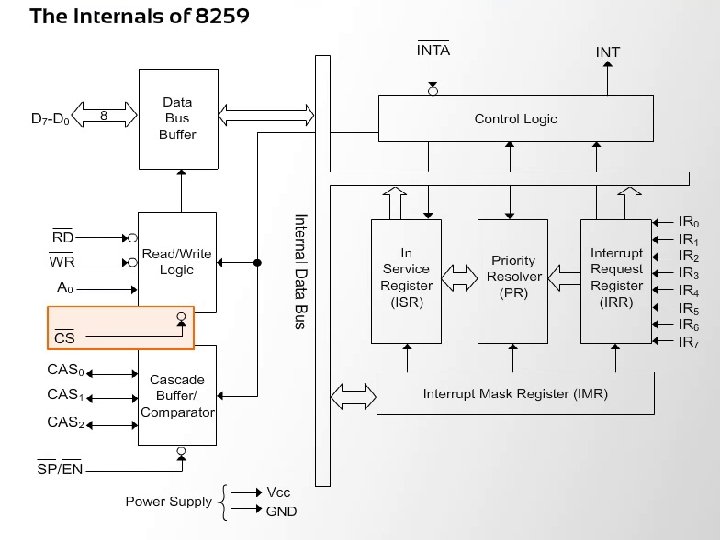
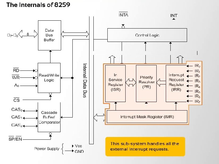
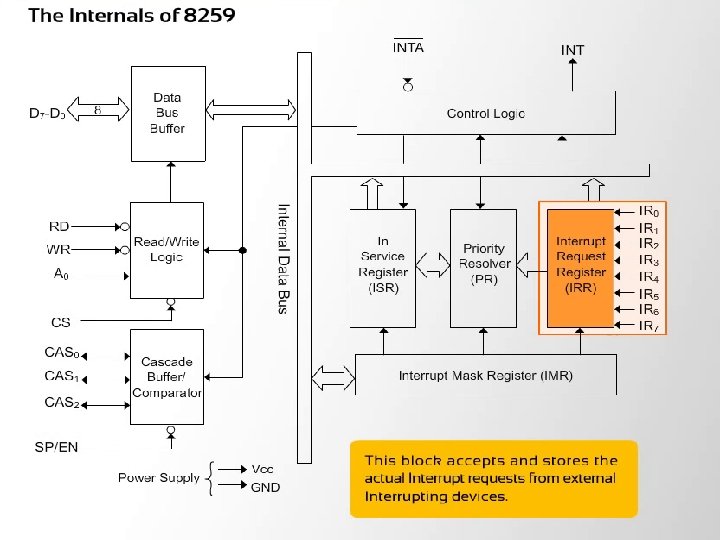
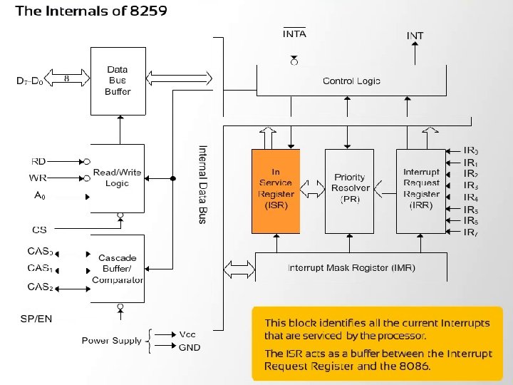
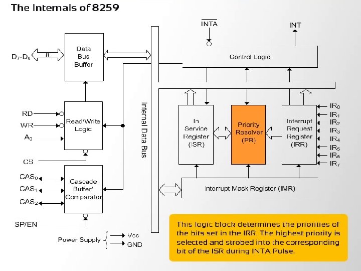
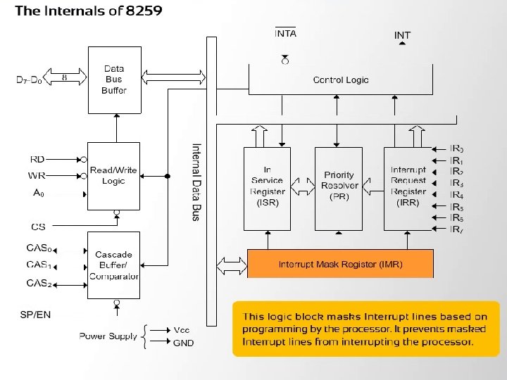
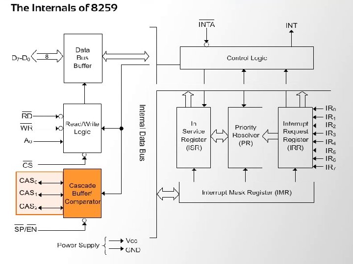
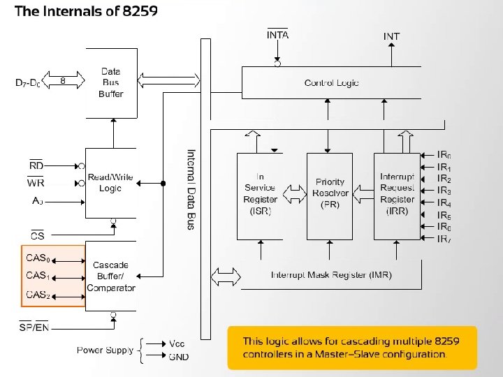
102 INTERRUPT CONTROLLER INTEL 8259
 1. This IC is designed to simplify the implementation")
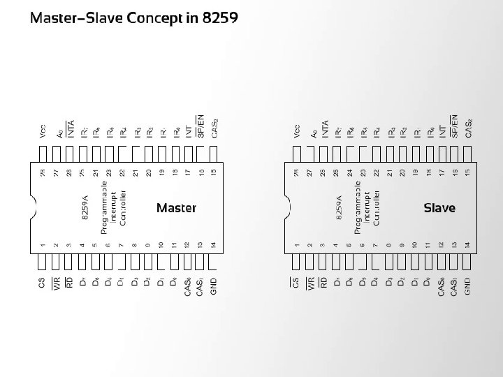
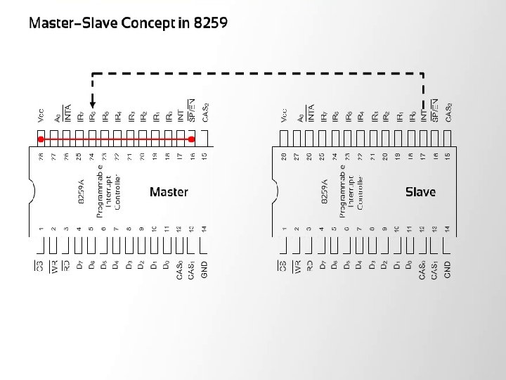
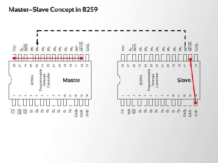
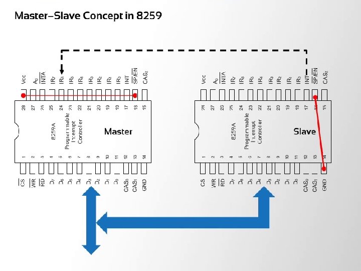
8259 Programmable Interrupt Controller (PIC) 1. This IC is designed to simplify the implementation of the interrupt interface in the 8088 and 8086 based microcomputer systems. 2. This device is known as a ‘Programmable Interrupt Controller’ or PIC. 3. It is manufactured using the NMOS technology and It is available in 28 -pin DIP. 4. The operation of the PIC is programmable under software control (Programmable)and it can be configured for a wide variety of applications. 5. 8259 A is treated as peripheral in a microcomputer system. 6. 8259 A PIC adds eight vectored priority encoded interrupts to the microprocessor. 7. This controller can be expanded without additional hardware to accept up to 64 interrupt request inputs. This expansion required a master 8259 A and eight 8259 A slaves. 8. Some of its programmable features are: · The ability to accept level-triggered or edge-triggered inputs. · The ability to be easily cascaded to expand from 8 to 64 interrupt-inputs. · Its ability to be configured to implement a wide variety of priority schemes.

8259 A PIC- PIN DIGRAM 8 2 5 9
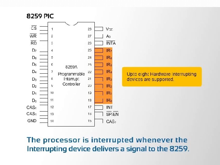

ASSINGMENT OF SIGNALS FOR 8259: 1. D 7 - D 0 is connected to microprocessor data bus D 7 -D 0 (AD 7 -AD 0). 2. IR 7 - IR 0, Interrupt Request inputs are used to request an interrupt and to connect to a slave in a system with multiple 8259 As. 3. WR - the write input connects to write strobe signal of microprocessor. 4. RD - the read input connects to the IORC signal. 5. INT - the interrupt output connects to the INTR pin on the microprocessor from the master, and is connected to a master IR pin on a slave. 6. INTA - the interrupt acknowledge is an input that connects to the INTA signal on the system. In a system with a master and slaves, only the master INTA signal is connected. 7. A 0 - this address input selects different command words within the 8259 A. 8. CS - chip select enables the 8259 A for programming and control. 9. SP/EN - Slave Program/Enable Buffer is a dual-function pin.

v When the 8259 A is in buffered mode, this pin is an output that controls the data bus transceivers in a large microprocessor-based system. v When the 8259 A is not in buffered mode, this pin programs the device as a master (1) or a slave (0). v CAS 2 -CAS 0, the cascade lines are used as outputs from the master to the slaves for cascading multiple 8259 As in a system.

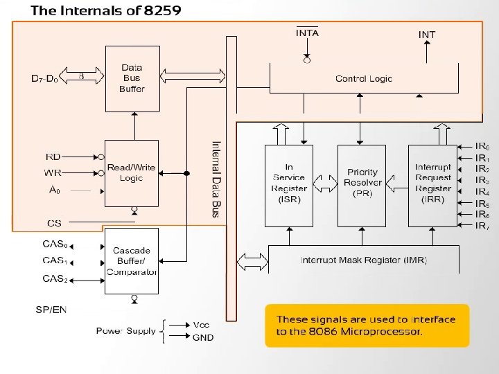
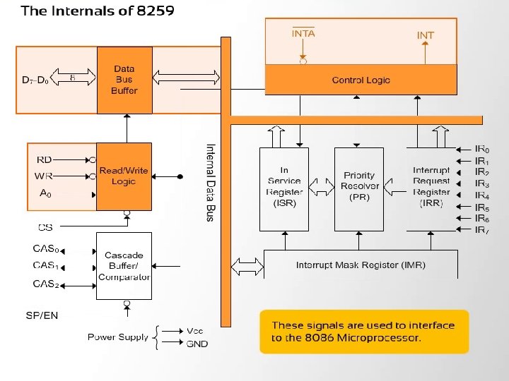
8259 A PIC- BLOCK DIAGRAM


Programming the 8259 A: The 82 C 59 A accepts two types of command words generated by the CPU: 1. Initialization Command Words (ICWs): Before normal operation can begin, each 82 C 59 A in the system must be brought to a starting point - by a sequence of 2 to 4 bytes timed by WR pulses. 2. Operational Command Words (OCWs): These are the command words which command the 82 C 59 A to operate in various interrupt modes. Among these modes are: a. Fully nested mode. b. Rotating priority mode. c. Special mask mode. d. Polled mode. The OCWs can be written into the 82 C 59 A anytime after initialization.

ICW 1: v To program this ICW for 8086 we place a logic 1 in bit IC 4. v Bits D 7, D 6 , D 5 and D 2 are don’t care for microprocessor operation and only apply to the 8259 A when used with an 8 -bit 8085 microprocessor. v This ICW selects single or cascade operation by programming the SNGL bit. If cascade operation is selected, we must also program ICW 3. v The LTIM bit determines whether the interrupt request inputs are positive edge triggered or level-triggered.

ICW 2: v Selects the vector number used with the interrupt request inputs. v For example, if we decide to program the 8259 A so that it functions at vector locations 08 H-0 FH, we place a 08 H into this command word. v Likewise, if we decide to program the 8259 A for vectors 70 H-77 H, we place a 70 H in this ICW.

ICW 3: v Is used only when ICW 1 indicates that the system is operated in cascade mode. v This ICW indicates where the slave is connected to the master. v For example, if we connected a slave to IR 2, then to program ICW 3 for this connection, in both master and slave, we place a 04 H in ICW 3. v Suppose we have two slaves connected to a master using IR 0 and IR 1. The master is programmed with an ICW 3 of 03 H; one slave is programmed with an ICW 3 of 01 H and the other with an ICW 3 of 02 H.

ICW 4: v Is programmed for use with the 8088/8086. This ICW is not programmed in a system that functions with the 8085 microprocessors. v The rightmost bit must be logic 1 to select operation with the 8086 microprocessor, and the remaining bits are programmed as follows:

Operation Command Words OCW 1: v Is used to set and read the interrupt mask register. v When a mask bit is set, it will turn off (mask) the corresponding interrupt input. The mask register is read when OCW 1 is read. v Because the state of the mask bits is known when the 8259 A is first initialized, OCW 1 must be programmed after programming the ICW upon initialization.

OCW 2: v Is programmed only when the AEOI mod is not selected for the 8259 A. v In this case, this OCW selects how the 8259 A responds to an interrupt. v The modes are listed as follows in next slide:

OCW 3: Ø Selects the register to be read, the operation of the special mask register, and the poll command. Ø If polling is selected, the P-bit must be set and then output to the 8259 A. The next read operation would read the poll word. The rightmost three bits of the poll word indicate the active interrupt request with the highest priority. Ø The leftmost bit indicates whethere is an interrupt, and must be checked to determine whether the rightmost three bits contain valid information.

8237 DMA CONTROLLER 135
 is a method of 136 allowing data to")
Introduction: � Direct Memory Access (DMA) is a method of 136 allowing data to be moved from one location to another in a computer without intervention from the central processor (CPU). �It is also a fast way of transferring data within (and sometimes between) computer. �The DMA I/O technique provides direct access to the memory while the microprocessor is temporarily disabled. �The DMA controller temporarily borrows the address bus, data bus and control bus from the microprocessor and transfers the data directly from the external devices to a series of memory locations (and vice versa).

The 8237 DMA controller • Supplies memory and I/O with control signals and addresses during DMA transfer • 4 -channels (expandable) – – 0: DRAM refresh 1: Free 2: Floppy disk controller 3: Free • 1. 6 MByte/sec transfer rate • 64 KByte section of memory address capability with single programming • “fly-by” controller (data does not pass through the DMA-only memory to I/O transfer capability) • Initialization involves writing into each channel: • i) The address of the first byte of the block of data that must be transferred (called the base address). • ii) The number of bytes to be transferred (called the word count). 137
 • RESET:")
8237 pins • CLK: System clock • CS΄: Chip select (decoder output) • RESET: Clears registers, sets mask register • READY: 0 for inserting wait states • HLDA: Signals that the μp has relinquished buses • DREQ 3 – DREQ 0: DMA request input for each channel • DB 7 -DB 0: Data bus pins • IOR΄: Bidirectional pin used during programming and during a DMA write cycle • IOW΄: Bidirectional pin used during programming and during a DMA read cycle • EOP΄: End of process is a bidirectional signal used as input to terminate a DMA process or as output to signal the end of the DMA transfer • A 3 -A 0: Address pins for selecting internal registers • A 7 -A 4: Outputs that provide part of the DMA transfer address • HRQ: DMA request output • DACK 3 -DACK 0: DMA acknowledge for each channel. • AEN: Address enable signal • ADSTB: Address strobe • MEMR΄: Memory read output used in DMA read cycle • MEMW΄: Memory write output used in DMA write cycle 138

8237 block diagram 139

Block Diagram Description 1. 2. 3. 4. 5. It containing Five main Blocks. Data bus buffer Read/Control logic block Priority resolver DMA channels. 140

DATA BUS BUFFER: It contain tristate , 8 bit bi-directional buffer. Slave mode , it transfer data between microprocessor and internal data bus. Master mode , the outputs A 8 -A 15 bits of memory address on data lines (Unidirectional). READ/CONTROL LOGIC: It control all internal Read/Write operation. Slave mode , it accepts address bits and control signal from microprocessor. Master mode , it generate address bits and control signal. 141

Control logic block 1. 2. 3. It contains , Control logic Mode set register and Status Register. CONTROL LOGIC: Master mode , It control the sequence of DMA operation during all DMA cycles. It generates address and control signals. It increments 16 bit address and decrement 14 bit counter registers. It activate a HRQ signal on DMA channel Request. Slave , mode it is disabled. 142

DMA controller details 143

Programming and applications Case studies 144 1. Traffic Light control 2. LED display 3. LCD display 4. Keyboard display interface 5. Alarm Controller

1. TRAFFIC LIGHT CONTROL 145

Traffic lights, which may also be known as stoplights, traffic lamps, traffic signals, signal lights, robots or semaphore, are signaling devices positioned at road intersections, pedestrian crossings and other locations to control competing flows of traffic. INTERFACING TRAFFIC LIGHT WITH 8086 The Traffic light controller section consists of 12 Nos. point led’s arranged by 4 Lanes in Traffic light interface card. Each lane has Go(Green), Listen(Yellow) and Stop(Red) LED is being placed. 146

LAN Direction SOUTH EAST NORTH WEST PWR 147 8086 LINES MODULES PA. 0 GO PA. 1 LISTEN PA. 2 STOP PA. 3 GO PA. 4 LISTEN PA. 5 STOP PA. 6 GO PA. 7 LISTEN PB. 0 STOP PB. 1 GO PB. 2 LISTEN PB. 3 STOP 13 -16 No Connection 17, 189 Supply from microcontroller 18, 20

CIRCUIT DIAGRAM TO INTERFACE TRAFFIC LIGHT WITH 8086 148

8086 ALP: 149 1100: START: MOV BX, 1200 H MOV CX, 0008 H MOV AL, [BX] MOV DX, CONTROL PORT OUT DX, AL INC BX NEXT: MOV AL, [BX] MOV DX, PORT A OUT DX, AL CALL DELAY INC BX LOOP NEXT JMP START DELAY: PUSH CX MOV CX, 0005 H REPEAT: MOV DX, 0 FFFFH LOOP 2: DEC DX JNZ LOOP 2 LOOP REPEAT POP CX RET

Lookup Table 1200 80 H 1201 21 H, 09 H, 10 H, 00 H (SOUTH WAY) 1205 0 CH, 09 H, 80 H, 00 H (EAST WAY) 1209 64 H, 08 H, 00 H, 04 H (NOURTH WAY) 120 D 24 H, 03 H, 02 H, 00 H (WEST WAY) 1211 END 150

2. LED DISPLAY 151
 is the most commonly used components, usually for displaying pins")
Light Emitting Diodes (LED) is the most commonly used components, usually for displaying pins digital states. Typical uses of LEDs include alarm devices, timers and confirmation of user input such as a mouse click or keystroke. INTERFACING LED Anode is connected through a resistor to GND & the Cathode is connected to the Microprocessor pin. So when the Port Pin is HIGH the LED is OFF & when the Port Pin is LOW the LED is turned ON. 152

PIN ASSIGNMENT WITH 8086 153

INTERFACE LED WITH 8255 154

8086 ALP LED interface 1100: START: MOV AL, 80 MOV DX, FF 36 OUT DX, AL BEGIN: MOV AL, 00 MOV DX, FF 30 OUT DX, AL CALL DELAY MOV AL, FF OUT DX, AL CALL DELAY JMP BEGIN DELAY: MOV CX, FFFF PO: DEC CX JNE PO RET 155

3. LCD DISPLAY 156

157

HARDWARE CONFIGURATION OF LCD WITH 8051/8086/8085 158
 J 1 Connector PORTS")
LCD INTERFACING WITH 8086 TRAINER KIT � GPIO- I (8255) J 1 Connector PORTS Control port PORT A PORT B PORT C ADDRESS FF 26 FF 20 FF 22 FF 24 �GPIO- I (8255) J 4 Connector PORTS Control port PORT A PORT B PORT C 159 ADDRESS FF 36 FF 30 FF 32 FF 34

160

LCD INTERFACING WITH 8051 Used in UNIT 5 also TRAINER KIT � GPIO- I (8255) J 1 Connector PORTS Control port PORT A PORT B PORT C 161 ADDRESS 4003 4000 4001 4002

162

4. Keyboard display interface 163

HARDWARE DESCRIPTION OF 8279 INTERFACE CARD Keyboard and display is configured in the encoded mode. In the encoded mode, a binary count sequence is put on the scan lines SL 0 -SL 3. These lines must be externally decoded to provide the scan lines for keyboard and display. A 3 to 8 decoder 74 LS 138 is provided for this purpose. The S 0 -S 1 output lines of this decoder are connected to the two rows of the keyboard. And QA 0 to QA 7 is connected to 7 Segment Display 164

165 PIN DIAGRAM OF 8279 PIN DIAGRAMOF 74 LS 138 Presented by C. GOKUL, AP/EEE , Velalar College of Engg & Tech, Erode

Detecting a Matrix Keyboard Key press 166

167

MVI A, 00 H Initialize keyboard/display in encoded OUT 81 H scan keyboard 2 key lockout mode MVI A, 34 H OUT 81 H Initialize prescaler count MVI A, 0 BH Load mask pattern to enable RST 7. 5 SIM mask other interrupts EI Enable Interrupt HERE: JMP HERE Wait for the interrupt Interrupt service routine MVI A, 40 H Initialize 8279 in read FIFO RAM mode OUT 81 H IN 80 H Get keycode MVI H, 62 H Initialize memory pointer to point MOV L, A 7 -Segment code MVI A, 80 H : Initialize 8279 in write display RAM mode OUT 81 H MOV A, M : Get the 7 segment code OUT 80 H : Write 7 -segment code in display RAM EI : Enable interrupt RET : Return to main program 168

169 5. ALARM CONTROLLER Relevant Material Not exact

HARDWARE DESCRIPTION OF RELAY & BUZZER INTERFACE 170

171 To interface Relay and Buzzer with 8086 Trainer Kit and To ON/OFF Relay and Buzzer card GPIO- I J 1 Connecter PORTS ADDRESS Control port FF 26 PORT A FF 20 PORT B FF 22 PORT C GPIO- II J 1 Connecter FF 24 PORTS ADDRESS Control port FF 36 PORT A FF 30 PORT B FF 32
- Slides: 171