8086 Pin diagram 8086 is a 40 pin


 0 1(HIGH) A 16/S 3 0 1 0 Characteristics")


 indicating 8086 is on")


 0 No operation 0 1 First Byte of")


 for")


")


 is a process in which an external device takes over")


- Slides: 83
8086 Pin diagram 8086 is a 40 pin DIP using MOS technology. It has 2 GND’s as circuit complexity demands a large amount of current flowing through the circuits, and multiple grounds help in dissipating the accumulated heat etc. 8086 works on two modes of operation namely, Maximum Mode and Minimum Mode.
Power Connections GND 1 40 8086 CLK 19 GND 20 VCC Pin Description: GND – Pin no. 1, 20 Ground CLK – Pin no. 19 – Type I Clock: provides the basic timing for the processor and bus controller. It is asymmetric with a 33% duty cycle to provide optimized internal timing. VCC – Pin no. 40 VCC: +5 V power supply pin
Address/ Data Lines AD 14 AD 13 AD 12 AD 11 AD 10 AD 9 AD 8 AD 7 AD 6 AD 5 AD 4 AD 3 AD 2 AD 1 AD 0 2 3 4 5 6 7 8 9 10 11 12 39 AD 15 8086 13 14 15 16 Continued…
Pin Description AD 15 -AD 0 – Pin no. 2 -16, 39 – Type I/O Address Data bus: These lines constitute the time multiplexed memory/ IO address (T 1) and data (T 2, T 3, TW, T 4) bus. A 0 is analogous to BHE* for the lower byte of the data bus, pins D 7 -D 0. It is low when a byte is to be transferred on the lower portion of the bus in memory or I/O operations. Eight –bit oriented devices tied to the lower half would normally use A 0 to condition chip select functions. These lines are active HIGH
Address Lines A 14 A 13 A 12 A 11 A 10 A 9 A 8 A 7 A 6 A 5 A 4 A 3 A 2 A 1 A 0 2 3 4 5 6 7 8 9 10 11 39 A 15 38 37 8086 36 35 12 13 14 15 16 Continued…
A 19/S 6, A 18/S 5, A 17/S 4, A 16/S 3 – Pin no. 35 -38 – Type O Address / Status: During T 1 these are the four most significant address lines for memory operations. During I/O operations these lines are low. During memory and I/O operations, status information is available on these lines during T 2, T 3, TW and T 4. The status of the interrupt enable FLAG bit (S 5) is updated at the beginning of each CLK cycle. A 17/S 4 and A 16/S 3 are encoded as shown. Continued…
A 17/S 4 0 (LOW) 0 1(HIGH) A 16/S 3 0 1 0 Characteristics Alternate Data Stack Code or None 1 S 6 is 0 (LOW) 1 Data This information indicates which relocation register is presently being used for data accessing.
Status Pins S 0 -S 7 8086 38 S 3 37 S 4 36 S 5 35 S 6 34 S 7 28 27 26 Continued…
Pin Description , , - Pin no. 26, 27, 28 – Type O Status: active during T 4, T 1 and T 2 and is returned to the passive state (1, 1, 1) during T 3 or during TW when READY is HIGH. This status is used by the 8288 Bus Controller to generate all memory and I/O access control signals. Any change by , or during T 4 is used to indicate the beginning of a bus cycle and the return to the passive state in T 3 or TW is used to indicate the end of a bus cycle. Continued…
These signals float to 3 -state OFF in “hold acknowledge”. These status lines are encoded as shown. S 2* S 1* S 0* Characteristics 0(LOW) 0 0 Interrupt acknowledge 0 0 1 Read I/O Port 0 1 0 Write I/O Port 0 1 1 Halt 1(HIGH) 0 0 Code Access 1 0 1 Read Memory 1 1 0 Write Memory 1 1 1 Passive Continued…
Status Details Indication 0 0 1 1 0 1 0 1 Interrupt Acknowledge Read I/O port Write I/O port Halt Code access Read memory Write memory Passive Continued…
S 4 S 3 Indications 0 0 Alternate data 0 1 Stack 1 0 Code or none 1 1 Data Continued…
----- Value of Interrupt Enable flag ----- Always low (logical) indicating 8086 is on the bus. If it is tristated another bus master has taken control of the system bus. ----- Used by 8087 numeric coprocessor to determine whether the CPU is a 8086 or 8088
Interrupts 8086 NMI 17 INTR 18 Pin Description: NMI – Pin no. 17 – Type I Non – Maskable Interrupt: an edge triggered input which causes a type 2 interrupt. A subroutine is vectored to via an interrupt vector lookup table located in system memory. NMI is not maskable internally by software. A transition from a LOW to HIGH initiates the interrupt at the end of the current instruction. This input is internally synchronized. Continued…
INTR – Pin No. 18 – Type I Interrupt Request: is a level triggered input which is sampled during the last clock cycle of each instruction to determine if the processor should enter into an interrupt acknowledge operation. A subroutine is vectored to via an interrupt vector lookup table located in system memory. It can be internally masked by software resetting the interrupt enable bit. INTR is internally synchronized. This signal is active HIGH.
Min mode signals 33 VCC 31 HOLD 30 HLDA 29 8086 28 27 26 25 ALE 24 Continued…
Pin Description HOLD, HLDA – Pin no. 31, 30 – Type I/O HOLD: indicates that another master is requesting a local bus “hold”. To be acknowledged, HOLD must be active HIGH. The processor receiving the “hold” request will issue HLDA (HIGH) as an acknowledgement in the middle of a T 1 clock cycle. Simultaneous with the issuance of HLDA the processor will float the local bus and control lines. After HOLD is detected as being LOW, the processor will LOWer the HLDA, and when the processor needs to run another cycle, it will again drive the local bus and control lines. The same rules as apply regarding when the local bus will be released. HOLD is not an asynchronous input. External synchronization should be provided if the system can not otherwise guarantee the setup time. Continued…
WR* - Pin no. 29 – Type O Write: indicates that the processor is performing a write memory or write I/O cycle, depending on the state of the M/IO* signal. WR* is active for T 2, T 3 and TW of any write cycle. It is active LOW, and floats to 3 -state OFF in local bus “hold acknowledge”. M/IO* - Pin no. 28 – type O Status line: logically equivalent to S 2 in the maximum mode. It is used to distinguish a memory access from an I/O access. M/IO* becomes valid in the T 4 preceding a bus cycle and remains valid until the final T 4 of the cycle (M=HIGH), IO=LOW). M/IO* floats to 3 -state OFF in local bus “hold acknowledge”. Continued…
DT/R* - Pin no. 27 – Type O Data Transmit / Receive: needed in minimum system that desires to use an 8286/8287 data bus transceiver. It is used to control the direction of data flow through the transceiver. Logically DT/R* is equivalent to S 1* in the maximum mode, and its timing is the same as for M/IO*. (T=HIGH, R=LOW). This signal floats to 3 -state OFF in local bus “hold acknowledge”. DEN* - Pin no. 26 – Type O Data Enable: provided as an output enable for the 8286/8287 in a minimum system which uses the transceiver. DEN* is active LOW during each memory and I/O access and for INTA cycles. For a read or INTA* cycle it is active from the middle of T 2 until the middle of T 4, while for a write cycle it is active from the beginning of T 2 until the middle of T 4. DEN* floats to 3 -state OFF in local bus “hold acknowledge”. Continued…
ALE – Pin no. 25 – Type O Address Latch Enable: provided by the processor to latch the address into the 8282/8283 address latch. It is a HIGH pulse active during T 1 of any bus cycle. Note that ALE is never floated. INTA* - Pin no. 24 – Type O INTA* is used as a read strobe for interrupt acknowledge cycles. It is active LOW during T 2, T 3 and TW of each interrupt acknowledge cycle.
Max mode signals 33 GND 31 30 29 8086 28 27 26 25 QS 0 24 QS 1 Continued…
Pin Description: RQ*/GT 0*, RQ*/GT 1* - Pin no. 30, 31 – Type I/O Request /Grant: pins are used by other local bus masters to force the processor to release the local bus at the end of the processor’s current bus cycle. Each pin is bidirectional with RQ*/GT 0* having higher priority than RQ*/GT 1*. RQ*/GT* has an internal pull up resistor so may be left unconnected. The request/grant sequence is as follows: Continued…
1. A pulse of 1 CLK wide from another local bus master indicates a local bus request (“hold”) to the 8086 (pulse 1) 2. During a T 4 or T 1 clock cycle, a pulse 1 CLK wide from the 8086 to the requesting master (pulse 2), indicates that the 8086 has allowed the local bus to float and that it will enter the “hold acknowledge” state at the next CLK. The CPU’s bus interface unit is disconnected logically from the local bus during “hold acknowledge”. 3. A pulse 1 CLK wide from the requesting master indicates to the 8086 (pulse 3) that the “hold” request is about to end and that the 8086 can reclaim the local bus at the next CLK. Continued…
Each master-master exchange of the local bus is a sequence of 3 pulses. There must be one dead CLK cycle after each bus exchange. Pulses are active LOW. If the request is made while the CPU is performing a memory cycle, it will release the local bus during T 4 of the cycle when all the following conditions are met: Ø Request occurs on or before T 2. Ø Current cycle is not the low byte of a word (on an odd address) Ø Current cycle is not the first acknowledge of an interrupt acknowledge sequence. Ø A locked instruction is not currently executing. Continued…
LOCK* - Pin no. 29 – Type O LOCK* : output indicates that other system bus masters are not to gain control of the system bus while LOCK* is active LOW. The LOCK* signal is activated by the “LOCK” prefix instruction and remains active until the completion of the next instruction. This signal is active LOW, and floats to 3 -state OFF in “hold acknowledge”. QS 1, QS 0 – Pin no. 24, 25 – Type O Queue Status: the queue status is valid during the CLK cycle after which the queue operation is performed. QS 1 and QS 0 provide status to allow external tracking of the internal 8086 instruction queue. Continued…
QS 1 QS 0 Characteristics 0(LOW) 0 No operation 0 1 First Byte of Op Code from Queue 1 (HIGH) 0 Empty the Queue 1 1 Subsequent byte from Queue
Common Signals Continued…
Pin Description: RD* - Pin no. 34, Type O Read: Read strobe indicates that the processor is performing a memory of I/O read cycle, depending on the state of the S 2 pin. This signal is used to read devices which reside on the 8086 local bus. RD* is active LOW during T 2, T 3 and TW of any read cycle, and is guaranteed to remain HIGH in T 2 until the 8086 local bus has floated. This signal floats to 3 -state OFF in “hold acknowledge”. READY – Pin no. 22, Type I READY: is the acknowledgement from the addressed memory or I/O device that it will complete the data transfer. The READY signal from memory / IO is synchronized by the 8284 A Clock Generator to form READY. This signal is active HIGH. The 8086 READY input is not synchronized. Correct operation is not guaranteed if the setup and hold times are not met. Continued…
TEST* - Pin No 23 – Type I TEST* : input is examined by the “Wait” instruction. If the TEST* input is LOW execution continues, otherwise the processor waits in an “idle” state. This input is synchronized internally during each clock cycle on the leading edge of CLK. RESET – Pin no. 21 – Type I Reset: causes the processor to immediately terminate its present activity. The signal must be active HIGH for at least four clock cycles. It restarts execution, as described in the instruction set description, when RESET returns LOW. RESET is internally synchronized. Continued…
BHE*/S 7 - Pin No. 34 – Type O Bus High Enable / Status: During T 1 the Bus High Enable signal (BHE*) should be used to enable data onto the most significant half of the data bus, pins D 15 -D 8. Eight bit oriented devices tied to the upper half of the bus would normally use BHE* to condition chip select functions. BHE* is LOW during T 1 for read, write, and interrupt acknowledge cycles when a byte is to be transferred on the high portion of the bus. The S, 7 status information is available during T 2, T 3 and T 4. The signal is active LOW and floats to 3 -state OFF in “hold”. It is LOW during T 1 for the first interrupt acknowledge cycle. BHE* A 0 Characteristics 0 0 Whole word 0 1 Upper byte from / to odd address 1 0 Lower byte from / to even address 1 1 None Continued…
MN/MX* - Pin no. 33 – Type - I Minimum / Maximum: indicates what mode the processor is to operate in. If the local bus is idle when the request is made the two possible events will follow: Ø Local bus will be released during the next clock. Ø A memory cycle will start within 3 clocks. Now the four rules for a currently active memory cycle apply with condition number 1 already satisfied.
Minimum Mode 8086 System DMUX MRD MWR IORD IOWR
A minimum mode of 8086 configuration depicts a stand alone system of computer where no other processor is connected. This is similar to 8085 block diagram with the following difference. The Data transceiver block which helps the signals traveling a longer distance to get boosted up. Two control signals data transmit/ receive are connected to the direction input of transceiver (Transmitter/Receiver) and DEN* signal works as enable for this block.
Read Cycle timing Diagram for Minimum Mode
In the bus timing diagram, data transmit / receive signal goes low (RECEIVE) for Read operation. To validate the data, DEN* signal goes low. The Address/ Status bus carries A 16 to A 19 address lines during BHE* (low) and for the remaining time carries Status information. The Address/Data bus carries A 0 to A 15 address information during ALE going high and for the remaining time it carries data. The RD* line going low indicates that this is a Read operation. The curved arrows indicate the relationship Continued… between valid data and RD* signal. The TW is Wait time needed to synchronize the fast processor with slow memory etc. The Ready pin is checked to see whether any peripheral needs more time for data transmission.
Write Cycle timing Diagram for Minimum Operation
This is the same as Read cycle Timing Diagram except that the DT/R* line goes high indicating it is a Data Transmission operation for the processor to memory / peripheral. Again DEN* line goes low to validate data and WR* line goes low, indicating a Write operation.
Bus Request & Bus Grant Timings in Minimum Mode System The HOLD and HLDA timing diagram indicates in Time Space HOLD (input) occurs first and then the processor outputs HLDA (Hold Acknowledge).
Maximum Mode 8086 System
In the maximum mode of operation of 8086, wherein either a numeric coprocessor of the type 8087 or another processor is interfaced with 8086. The Memory, Address Bus, Data Buses are shared resources between the two processors. The control signals for Maximum mode of operation are generated by the Bus Controller chip 8788. The three status outputs S 0*, S 1*, S 2* from the processor are input to 8788. The outputs of the bus controller are the Control Signals, namely DEN, DT/R*, IORC*, IOWTC*, MRDC*, ALE etc. These control signals perform the same task as the minimum mode operation. However the DEN is an active HIGH signal which has to be converted to active LOW by means of an inverter.
Here MRDC* signal is used instead of RD* as in case of Minimum Mode S 0* to S 2* are active and are used to generate control signal. Memory Read timing in Maximum Mode
Here the maximum mode write signals are shown. Please note that the T states correspond to the time during which DEN* is LOW, WRITE Control goes LOW, DT/R* is HIGH and data output in available from the processor on the data bus. Memory Write Timing in Maximum Mode
RQ*/ GT* Timings in Maximum Mode Request / Grant pin may appear that both signals are active low. But in reality, Request signal goes low first (input to processor), and then the processor grants the request by outputting a low on the same pin.
8284 Clock Generator The clock Generator 8284 performs the following tasks in addition to generating the system clock for the 8086/8088. ü Generating the Ready signal for h 8086/8088 ü Generating the Reset signal for h 8086/8088
8284 Block Diagram TANK CSYNC X 1 X 2 EFI OSC CLOCK LOGIC PCLK READY LOGIC READY CLK RDY 1 RDY 2 RESET LOGIC RESET
8284 Pin Diagram CSYNC 1 18 VCC PCLK 2 17 X 2 3 16 X 1 RDY 1 4 15 TANK READY 5 14 EFI RDY 2 6 8284 13 7 12 CLK 8 11 GND 9 10 OSC RESET
Clock Logic Continued…
The clock logic generates the three output signals OSC, CLOCK, and PCLK. OSC: OSC is a TTL clock signal generated by the crystal oscillator in 8284. Its frequency is same as the frequency of the crystal connected between X 1 and X 2 pins of 8284. In a PC, a crystal of 14. 31 MHz is connected between X 1 and X 2. thus OSC output frequency will be 14. 31 MHz. This signal is used by the Color Graphics Adapter (CGA). The Tank input is used by the crystal oscillator only if the crystal is an overtone type crystal. An LC circuit is connected to the TANK input to tune the oscillator to the overtone frequency of the crystal. Generally, in PCs, the TANK input is connected to ground, as fundamental type crystal is used in a PC. Continued…
Clock: The Clock output of 8284 is used as the system clock for the 8086/8088, 8087, and the bus controller 8288. It is having a duty cycle of 33%. It is derived from the OSC frequency generated by the crystal oscillator, or from an External Frequency Input (EFI). These two signals are inputs to a multiplexer. The F/C* (external frequency/crystal) input to the multiplexer decides this aspect. If F/C*=0, OSC frequency is used for deriving Clock. If F/C*=1, EFI input is used for deriving clock. The output of the multiplexer, which is OSC or EFI, is divided by 3 to provide the Clock output. Thus, if F/C*=0, clock frequency will be 14. 31 MHz/3=4. 77 MHz. Continued…
Turbo PCs use 30 MHz crystal oscillator circuit for generating EFI input. With F/C*=1, they allow turbo clock speed of 10 MHz. Such PCs provide a choice of switching between 4. 77 MHz and 10 MHz using a toggle switch or manual operation. The switching can also be controlled by software using an output port. The CSYNC input is a synchronization signal for synchronizing multiple 8284 s in a system. In a PC, CSYNC is tied to ground, as there is a single 8284. Continued…
PCLK: PCLK frequency output is obtained by dividing clock frequency by 2. PCLK is used by support chips like 8254 timer, which need a lower frequency for their operation. Continued…
Pin functions of 8284 A: X 1 and X 2 The Crystal Oscillator pins connect to an external crystal used as the timing source for the clock generator and all its functions. EFI The External Frequency input is used when the F/C is pulled high. EFI supplies the timing whenever the F/C* pin is high. F/C* The Frequency/Crystal select input results the clocking source for the 8284 A. If this pin is held high, an external clock is provided to the EFI input pin, and if it is held low, the internal crystal oscillator provides the timing signal. Continued…
CSYNC The clock synchronization pin is used whenever the EFI input provides synchronization in systems with multiple processors. When the internal crystal oscillator is used, this pin must be grounded. OSC The Oscillator output is a TTL level signal that is at the same frequency as the crystal or EFI input. (The OSC output provides and EFI input to other 8284 A clock generators in some multiple processor systems). Continued…
CLK The clock output pin provides CLK input signal to the 8086/8088 microprocessors (and other components in the system). The CLK pin has an output signal that is one-third of the crystal or EFI input frequency and has a 33 percent duty cycle, which is required by the 8086/8088. PCLK The Peripheral Clock signal is one-sixth the crystal or EFI input frequency and has a 50 percent duty cycle. The PCLK output provides a clock signal o the peripheral equipment in the system.
Clock Generator (8284 A and the 8086/8088 microprocessor illustrating the connection for the clock and reset signals (A 15 MHz crystal provides the 5 MHz clock for the microprocessor)
Ready Logic The Ready Logic generates the Ready signal for the 8086/8088. If the Ready signal is made low by this circuit during T 2 state of a machine cycle, the microprocessor introduces a wait state between T 3 and T 4 states of the machine cycle. Continued…
The Ready logic is indicated in the figure. There are two pairs of signals in 8284 which can make the Ready output of 8284 to go low. If (RDY 1=0 or SEN 1*=1) and (RDY 2=0 or AEN 2*=1), the Ready output becomes low when the next clock transition takes place. In PCs, RDY 2 and AEN 2* are not used, and as such RDY 2 is tied to Ground and /or AEN 2* is tied to +5 V. AEN 1* is used for generating wait states in the 8086/8088 bus cycle, and RDY 1 is used for generating wait state in the DMA bus cycle.
Reset Logic Continued…
Reset Logic The Reset logic generates the Reset input signal for the 8086/8088. When the RESET* pin goes low, the Reset output is generated by the 8284 when the next clock transition takes place. In PCs, the RES* input is activated by one of the following. ü From the manual Reset button on the front panel. ü From the ‘Power on Reset’ circuit, which uses RC components. ü If the ‘Power Good’ signal from the SMPS is not active.
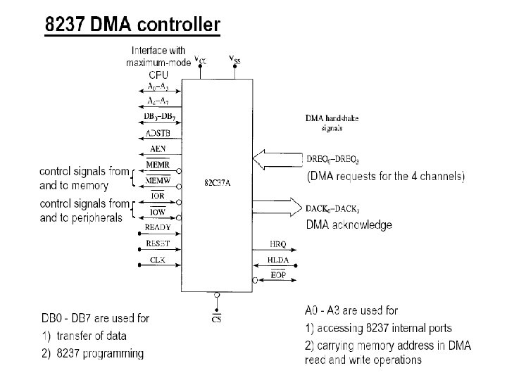
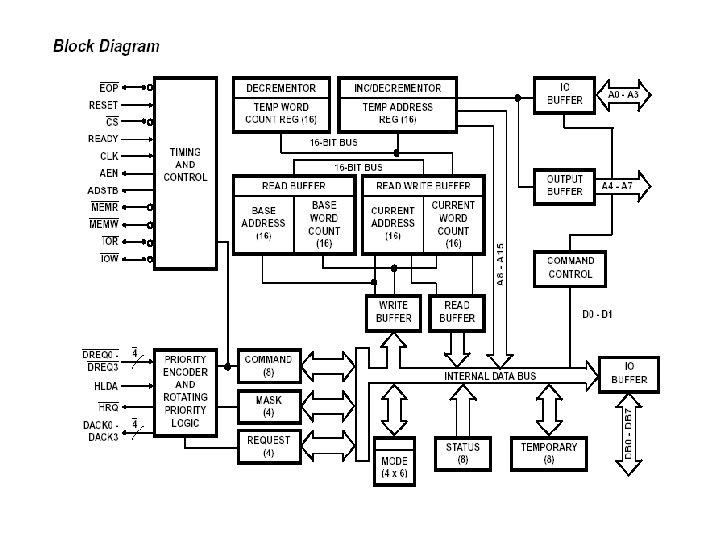
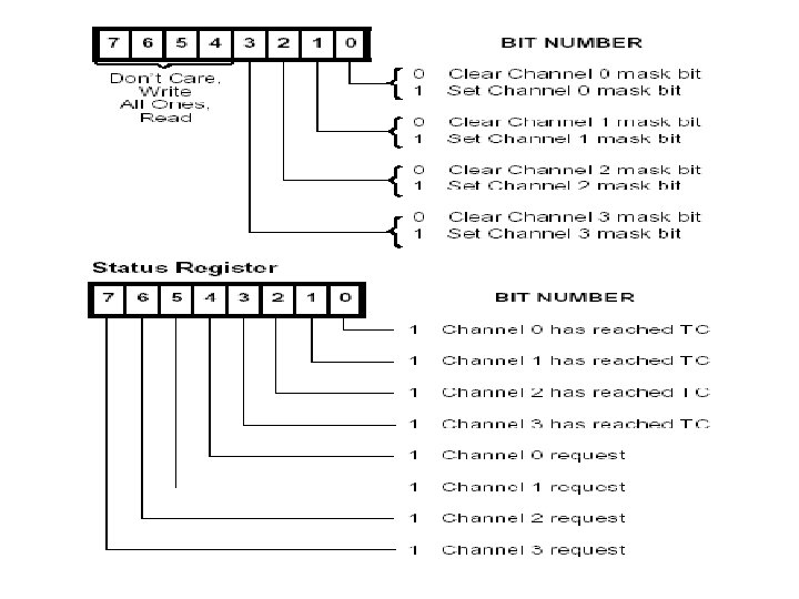
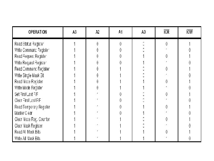
8237 DMA Controller
Address Size Expansion: (32 X 4 RAM module using 8 X 4 RAM chips) ACOE 255 Microprocessors I - Frederick University 61
Memory Maps • Tables that show the addresses occupied by each memory device in a system. • In the previous example it is assumed that the processor has only 7 address line, thus it can address 128 memory locations. • The size of the RAM memory module is 32 bytes, thus the module can be mapped to occupy one out of the four available memory blocks in the memory map. • The memory block occupied by the memory module depends on the connection of the address selection circuit (AND gate) that enables the decoder. ACOE 255 Microprocessors I - Frederick University 62
Effect of the Address Selection Circuit • The memory block occupied by the memory module depends on the connection of the address selection circuit (AND gate) that enables the decoder. • Two address lines are used to control the address selection circuit, thus the circuit can be configured to occupy four different areas in the address space. ACOE 255 Microprocessors I - Frederick University 63
Example: (32 X 4 RAM module using 8 X 4 RAM chips - Assume an 8 -address line processor) ACOE 255 Microprocessors I - Frederick University 64
Memory Map for previous example. • There are three address lines connected on the address selection circuit. Thus there can be eight different memory map configurations. • Three possible memory map configurations are shown below. ACOE 255 Microprocessors I - Frederick University 65
Design Example: Design an 8 KX 8 RAM module using 2 KX 8 RAM chips. The module should be connected on an 8 -bit processor with a 16 -bit address bus, and occupy the address range starting from the address A 000. Show the circuit and the memory map. • Number of memory devices needed = 8 K/2 K = 4 • Decoder needed = 2 X 4 • Number of address lines on each 2 KX 8 memory chip = 11 2 m = 2 K = 21 x 210 = 211 (A 0. . A 10) • Decoder needed = 2 X 4 2 address lines are needed for the decoder. (A 11. . A 12) • Number of address lines needed for the address selection circuit = 16 - 11 - 2 = 3 (A 13, A 14 A 15) ACOE 255 Microprocessors I - Frederick University 66
Circuit Diagram ACOE 255 Microprocessors I - Frederick University 67
Address Decoding • The physical address space, or memory map, of a microprocessor refers to the range of addresses of memory location that can accessed by the microprocessor. The size of the address space depends on the number of address lines of the microprocessor. • At least two memory devices are required in a microprocessor system: one for the ROM and one for the RAM. • In an 8088/8086 the high addresses in the memory map should always be occupied by a ROM, while the low addresses in the memory map should always be occupied by a RAM. • Address decoding is required in order to enable the connection of more than one memory devices on the microprocessor. Each device will occupy a unique area in the memory map. • A memory system is not fully decoded if some of the address lines are not used by the address decoding circuit or memory. In this case a memory device will occupy more than one sections in the memory map. This is referred as memory mirroring or memory imaging. ACOE 255 Microprocessors I - Frederick University 68
Address Decoding Circuits • A number of types of address decoding circuits can be used in a microprocessor system. The main issues related to the selection of an address decoding circuit are: – The time delays introduced by the address decoding circuit. This delays are added to the access time of the memory devices, and might yield to the insertion of wait states. – The number of chips required by the address decoding circuit, as well as the complexity of the circuit (number of tracks required on the board. • An address decoding circuit must ensure that an address section is occupied by only one memory device. If two or more devices occupy the same addresses then bus contention will occur. Bus contention occurs if two of more devices drive the bus at the same time. Bus contention can be either static or dynamic. – Static bus contention occurs when two or more devices drive a bus for a prolonged time period. This might damage some of the components of the system. Static bus contention might be caused by improper address decoding design, or by other faults in the system such as a short circuit of the CS of a device to the ground. – Dynamic bus contention occurs when two or more devices drive a bus for a short period of time. This might change the logic levels on the bus and cause system malfunctions. Dynamic bus contention might be caused by improper address decoding design, or by wrong memory timing analysis. ACOE 255 Microprocessors I - Frederick University 69
Address decoding circuits using Only NAND gates • A single NAND gate is used to decode each memory device. The inputs of the NAND gate can be connected on the address lines either directly, or through inverters, according to the required memory map. • This decoding circuit has the advantage that it adds a short time delay in the memory path. (td = 2 X gate delay <10 ns) • The disadvantage of this circuit is that too many gates (NAND and NOT) are needed for memory systems that have a few memory chips. This increases the cost of the system, adds to the complexity of the PCB board (too many chips and lines) and might create fanout problems. ACOE 255 Microprocessors I - Frederick University 70
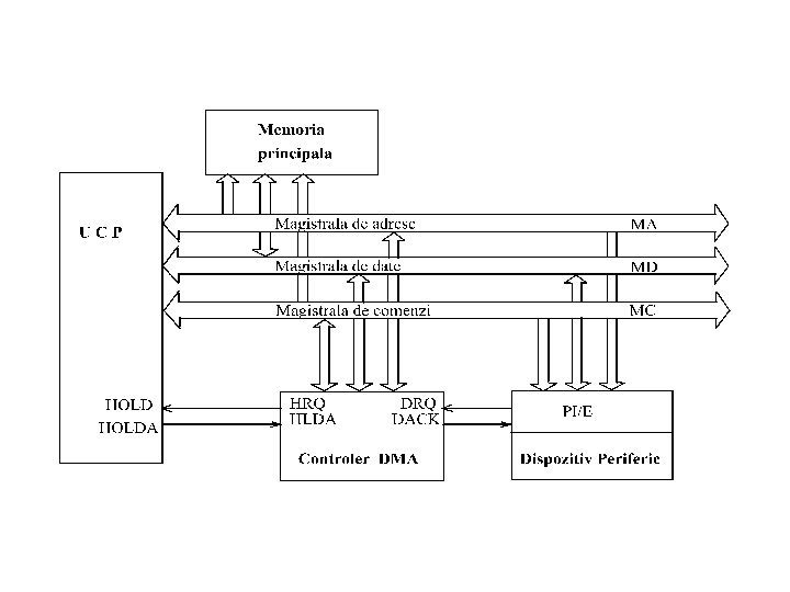
Direct memory access (DMA) is a process in which an external device takes over the control of system bus from the CPU. DMA is for high-speed data transfer from/to mass storage peripherals, e. g. harddisk drive, magnetic tape, CD-ROM, and sometimes video controllers. For example, a hard disk may boasts a transfer rate of 5 M bytes per second, i. e. 1 byte transmission every 200 ns. To make such data transfer via the CPU is both undesirable and unnecessary. The basic idea of DMA is to transfer blocks of data directly between memory and peripherals. The data don’t go through the microprocessor but the data bus is occupied. “Normal” transfer of one data byte takes up to 29 clock cycles. The DMA transfer requires only 5 clock cycles. Nowadays, DMA can transfer data as fast as 60 M byte per second. The transfer rate is limited by the speed of memory and peripheral devices.
Basic process of DMA For 8086 in maximum mode: The RQ/GT 1 and RQ/GT 0 pins are used to issue DMA request and receive acknowledge signals. Sequence of events of a typical DMA process 1) Peripheral asserts one of the request pins, e. g. RQ/GT 1 or RQ/GT 0 (RQ/GT 0 has higher priority) 2) 8088 completes its current bus cycle and enters into a HOLD state 3) 8088 grants the right of bus control by asserting a grant signal via the same pin as the request signal. 4) DMA operation starts 5) Upon completion of the DMA operation, the peripheral asserts the request/grant pin again to relinquish bus control. For 8086 in minimum mode: The HOLD and HLDA pins are used instead to receive and acknowledge the hold request respectively. Normally the CPU has full control of the system bus. In a DMA operation, the peripheral takes over bus control temporarily.
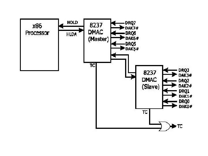
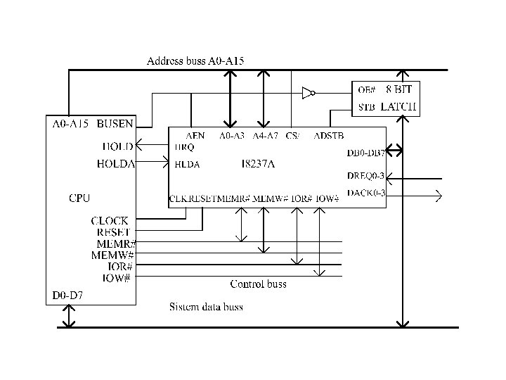
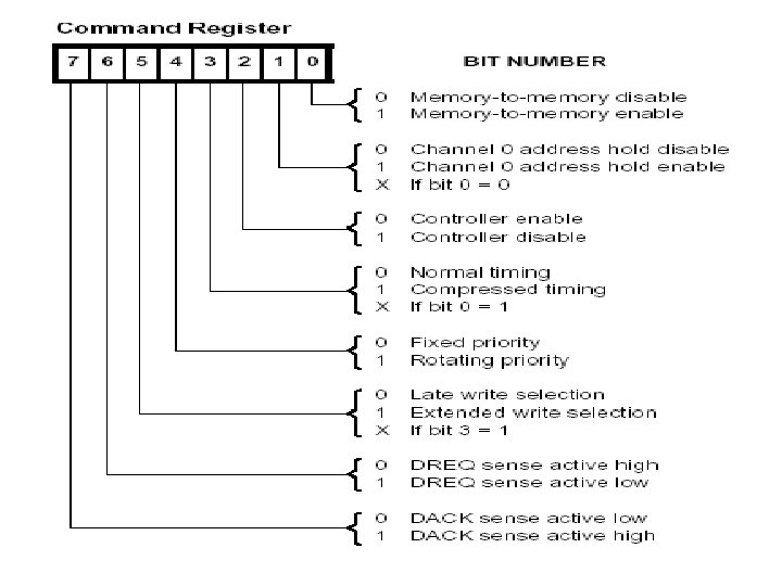
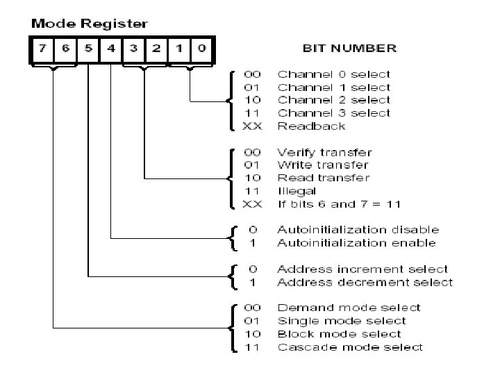
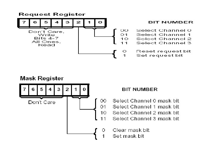
DMA controller A DMA controller interfaces with several peripherals that may request DMA. The controller decides the priority of simultaneous DMA requests communicates with the peripheral and the CPU, and provides memory addresses for data transfer. DMA controller commonly used with 8088 is the 8237 programmable device. The 8237 is in fact a special-purpose microprocessor. Normally it appears as part of the system controller chip-sets. The 8237 is a 4 -channel device. Each channel is dedicated to a specific peripheral device and capable of addressing 64 K bytes section of memory.