DMA Direct Memory Access Introduction to 8237 DMA


 • Single Bus, Detached DMA controller • Each transfer uses bus")
 • Single Bus, Integrated DMA controller • Controller may support >1")
 • Separate I/O Bus • Bus supports all DMA enabled devices")


: Used")
: Enables the DMA address latch")
: bi-dir Used as an input")


 0001 = Base")


- Slides: 42
DMA Direct Memory Access Introduction to 8237
DMA Action Memory CPU Data – Address - Control Handshaking DMA
Three Techniques for Input of a Block of Data
Simple Interrupt Processing Push FLAG and CS and IP Pop FLAG and CS and IP Load new CS and IP and set FLAG
Changes in Memory and Registers for an Interrupt
DMA and Interrupt Breakpoints During an Instruction Cycle
DMA is for high-speed data transfer from/to mass storage peripherals, e. g. harddisk drive, magnetic tape, CD-ROM, and sometimes video controllers. For example, a hard disk may boasts a transfer rate of 5 M bytes per second, i. e. 1 byte transmission every 200 ns. To make such data transfer via the CPU is both undesirable and unnecessary. The basic idea of DMA is to transfer blocks of data directly between memory and peripherals. The data don’t go through the microprocessor but the data bus is occupied. “Normal” transfer of one data byte takes up to 29 clock cycles. The DMA transfer requires only 5 clock cycles. Nowadays, DMA can transfer data as fast as 60 M byte per second. The transfer rate is limited by the speed of memory and peripheral devices.
Typical DMA Module Diagram
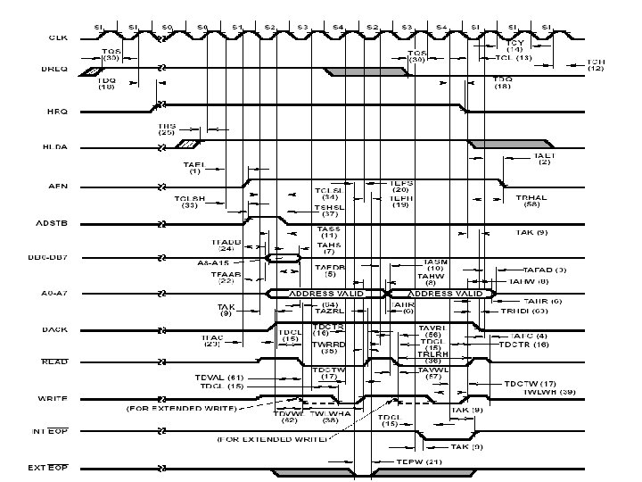
Basic process of DMA In maximum mode: Handshaking Pins: RQ/GT 1 and RQ/GT 0 DMA request and acknowledge Sequences: 1) Peripheral asserts one of the request pins, e. g. RQ/GT 1 or RQ/GT 0 (RQ/GT 0 has higher priority) 2) CPU completes its current bus cycle and enters into a HOLD state 3) CPU grants the right of bus control by asserting a grant signal via the same pin as the request signal. 4) DMA operation starts 5) Upon completion of the DMA operation, the peripheral asserts the request/grant pin again to relinquish bus control. In minimum mode: The HOLD and HLDA pins are used for handshaking
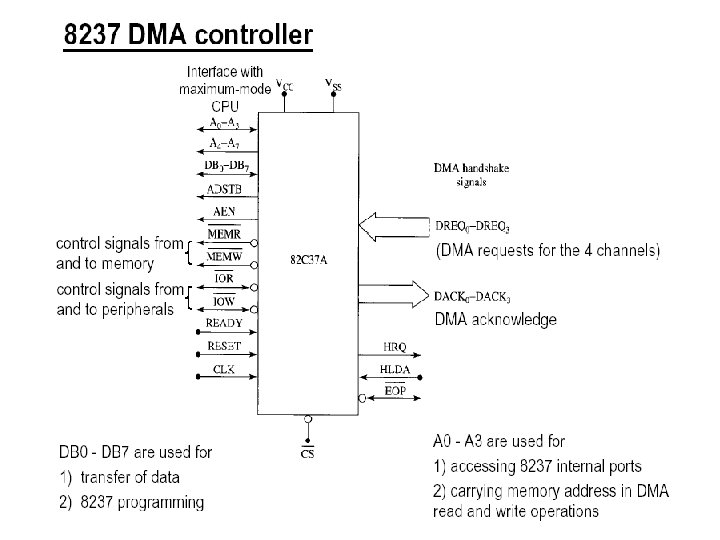
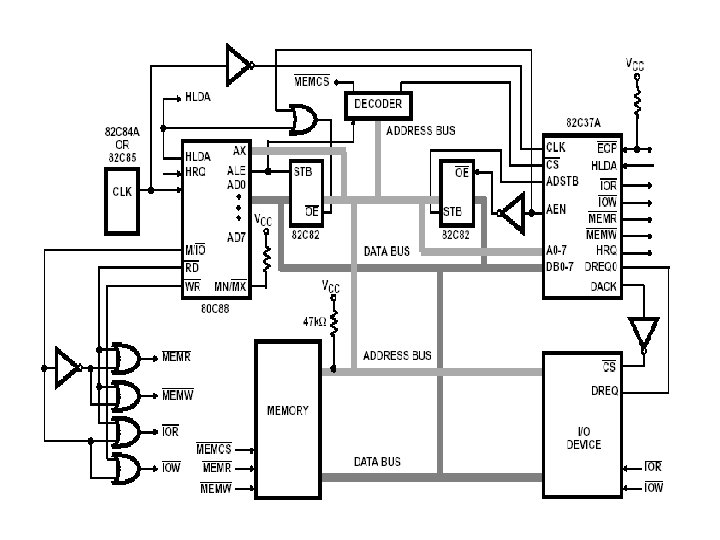
DMA Controller A DMA controller interfaces with several peripherals that may request DMA. The controller decides the priority of simultaneous DMA requests communicates with the peripheral and the CPU, and provides memory addresses for data transfer. DMA controller commonly used with 8086 is the 8237 programmable device. The 8237 is in fact a special-purpose microprocessor. Normally it appears as part of the system controller chip-sets. The 8237 is a 4 -channel device. Each channel is dedicated to a specific peripheral device and capable of addressing 64 K bytes section of memory.
DMA Configurations (1) • Single Bus, Detached DMA controller • Each transfer uses bus twice – I/O to DMA then DMA to memory • CPU is suspended twice
DMA Configurations (2) • Single Bus, Integrated DMA controller • Controller may support >1 device • Each transfer uses bus once – DMA to memory • CPU is suspended once
DMA Configurations (3) • Separate I/O Bus • Bus supports all DMA enabled devices • Each transfer uses bus once – DMA to memory • CPU is suspended once
System Data Bus
DMA Transfer Cycle Stealing • DMA controller takes over bus for a cycle • Transfer of one word of data • Not an interrupt – CPU does not switch context • CPU suspended just before it accesses bus – i. e. before an operand or data fetch or a data write • Slows down CPU but not as much as CPU doing transfer
Intel 8237 A DMA Controller • • • Interfaces to 80 x 86 family and DRAM When DMA module needs buses it sends HOLD signal to processor CPU responds HLDA (hold acknowledge) – • DMA module can use buses E. g. transfer data from memory to disk 1. Device requests service of DMA by pulling DREQ (DMA request) high 2. DMA puts high on HRQ (hold request), 3. CPU finishes present bus cycle (not necessarily present instruction) and puts high on HDLA (hold acknowledge). HOLD remains active for duration of DMA 4. DMA activates DACK (DMA acknowledge), telling device to start transfer 5. DMA starts transfer by putting address of first byte on address bus and activating MEMR; it then activates IOW to write to peripheral. DMA decrements counter and increments address pointer. Repeat until count reaches zero 6. DMA deactivates HRQ, giving bus back to CPU
DMA Some important signal pins: • DREQ 3 – DREQ 0 (DMA request): Used to request a DMA transfer for a particular DMA channel. • DACK 3 – DACK 0 (DMA channel acknowledge): Acknowledges a channel DMA request from a device. • HRQ (Hold request): Requests a DMA transfer. • HLDA (Hold acknowledge) signals the 8237 that the microprocessor has relinquished control of the address, data and control buses.
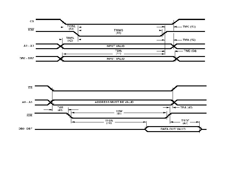
DMA Some important signal pins: • AEN (Address enable): Enables the DMA address latch connected to the 8237 and disable any buffers in the system connected to the microprocessor. (Use to take the control of the address bus from the microprocessor) • ADSTB (Address strobe): Functions as ALE to latch address during the DMA transfer. • EOP (End of process): bi direction, Signals the end of the DMA process. • IOR (I/O read): bi-dir, Used as an input strobe to read data from the 8237 during programming and used as an output strobe to read data from the port during a DMA write cycle.
DMA Some important signal pins: • IOW (I/O write): bi-dir Used as an input strobe to write data to the 8237 during programming and used as an output strobe to write data to the port during a DMA read cycle. • MEMW (Memory write): Used as an output to cause memory to write data during a DMA write cycle. • MEMR (Memory read): Used as an output to cause memory to read data during a DMA read cycle • A 3 – A 0 : address pins select an internal register during programming and provide part of the DMA transfer address during DMA operation.
DMA Some important signal pins: • A 7 – A 4 : address pins are outputs that provide part of the DMA transfer address during a DMA operation. • DB 0 – DB 7 : data bus, connected to microprocessor and are used during the programming DMA controller.
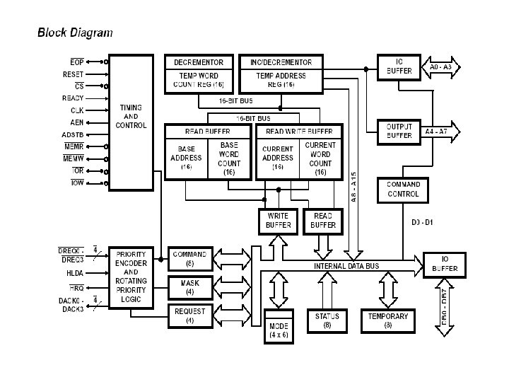
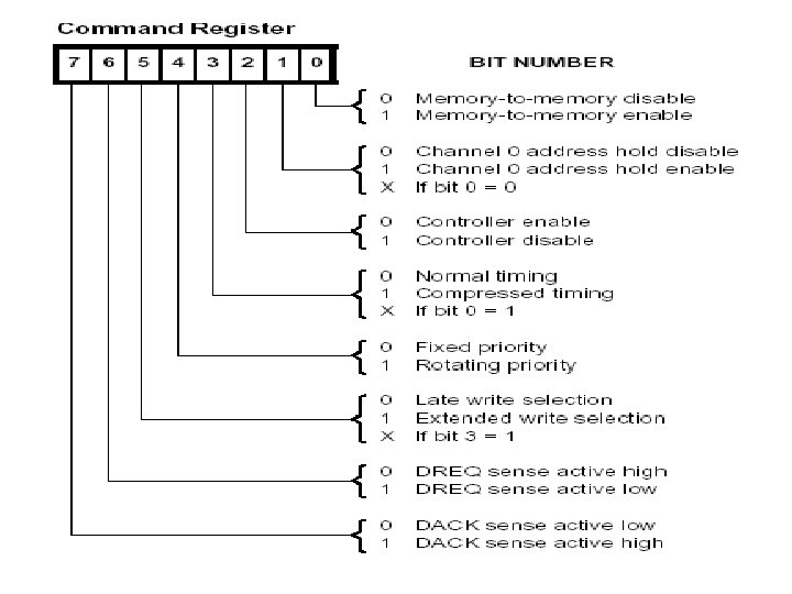
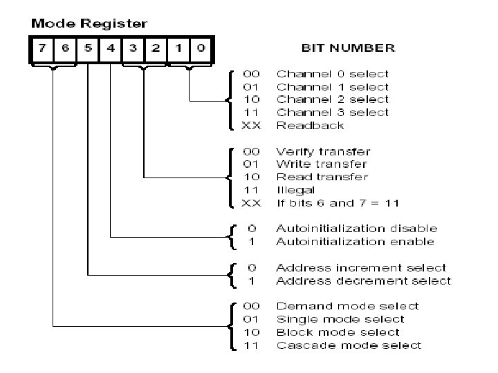
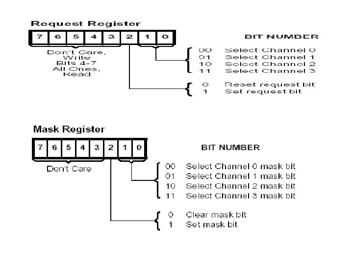
Internal registers: • CAR : The current address register, is used to hold the 16 -bit memory address used for the DMA transfer. • CWCR : The current word count register, programs a channel for the number of bytes (up to 64 K) transferred during a DMA action. • BA & BWC : The base address and base word count , registers are used when auto-initialization is selected for a channel. In this mode, their contents will be reloaded to the CAR and CWCR after the DMA action is completed. • The command register (CR) programs the operation of the 8237 DMA controller • Each channel has its own CAR, CWCR, BA and BWC.
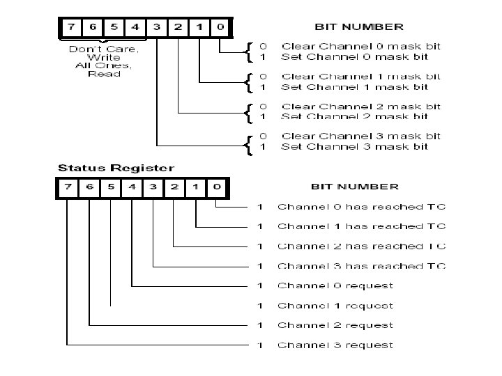
• MR : The mode register, programs the mode of operation for a channel. Each channels has its own mode register (RD/WR-INC/DEC. . ) • RR : The request register, is used to request a DMA transfer via software, which is very useful in memory-to-memory Transfers where external signals is not available for DMA transfer • MRSR : The mask register set/reset, sets or clears the channel mask to disable or enable particular DMA channels. If the mask is set, The channel is disabled • MSR : The mask register, clears or sets all of the masks with one command instead of individual channels as with the MRSR. • SR : The status register, shows the status of each DMA channel. TC Bits indicate, terminal count
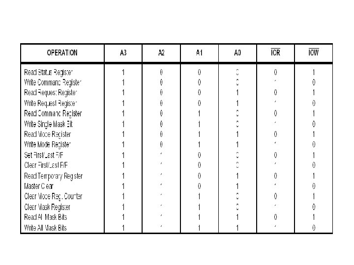
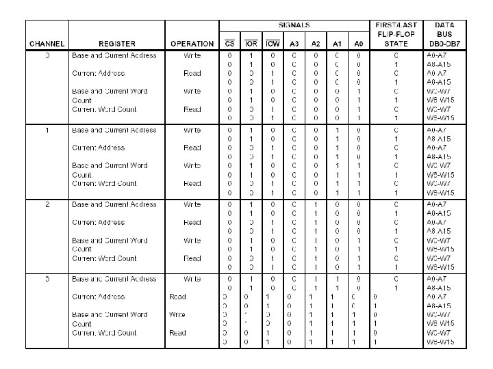
Addresses • • 0000 = Base and Current Address (Ch 0) 0001 = Base and Current Word (Ch 0) 0010 = Base and Current Address (Ch 1) 0011 = Base and Current Word (Ch 1) 0100 = Base and Current Address (Ch 2) 0101 = Base and Current Word (Ch 2) 0110 = Base and Current Address (Ch 3) 0111 = Base and Current Word (Ch 3)
Addresses • • 1000 = RD Status / WR Command 1001 = Request Register 1010 = RD Command / WR single Mask bit 1011 = Mode Register 1100 = Set/ Clear Last F/F 1101 = Read Temp Register / Master clear 1110 = CLR mode , counter / clear mask 1111 = All Masks bit
Data Transfer modes: Single Transfer Mode • In Single Transfer mode the device is programmed to make one transfer only. • The word count will be decremented and the address decremented or incremented following each transfer. • When the word count ``rolls over'' from zero to FFFFH, a Terminal Count (TC) will cause an Auto initialize if the channel has been programmed to do so.
Block Transfer Mode • In Block Transfer mode the device is activated by DREQ to continue making transfers during the service until a TC, caused by word count going to FFFFH, or an external End of Process (EOP) is encountered. • DREQ need only be held active until DACK becomes active. Again, an Autoinitialization will occur at the end of the service if the channel has been programmed for it.
Demand Transfer Mode: • In Demand Transfer mode the device is programmed to continue making transfers until a TC or external EOP is encountered or until DREQ goes inactive. • Transfers may continue until the I/O device has exhausted its data capacity. the DMA service can be re-established by means of a DREQ. • During the time between services when the microprocessor is allowed to operate, the intermediate values of address and word count are stored in the 8237 A Current Address and Current Word Count registers. • EOP can cause an Autoinitialize at the end of the service. EOP is generated either by TC or by an external signal.
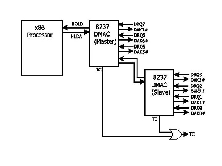
DMA Cascade Mode: • more than one 8237 A together for simple system expansion. • The HRQ and HLDA signals from the additional 8237 A are connected to the DREQ and DACK signals of a channel of the initial 8237 A. • This allows the DMA requests of the additional device to propagate through the priority network circuitry of the preceding device. Advanced Microprocessor 33