Photodetectors Content Physical Principles of Photodiodes pin APD
![Responsivity • The primary photocurrent resulting from absorption is: [6 -3] • Quantum Efficiency: Responsivity • The primary photocurrent resulting from absorption is: [6 -3] • Quantum Efficiency:](https://slidetodoc.com/presentation_image_h/098fa700395b8fb2a060d54b7b23bec8/image-7.jpg)
![Noise calculation (1) • Quantum noise current (lower limit on the sensitivity): [6 -11] Noise calculation (1) • Quantum noise current (lower limit on the sensitivity): [6 -11]](https://slidetodoc.com/presentation_image_h/098fa700395b8fb2a060d54b7b23bec8/image-15.jpg)
![Noise calculation (2) • The total rms photodetector noise current is: [6 -14] • Noise calculation (2) • The total rms photodetector noise current is: [6 -14] •](https://slidetodoc.com/presentation_image_h/098fa700395b8fb2a060d54b7b23bec8/image-16.jpg)
- Slides: 23

Photodetectors

Content • Physical Principles of Photodiodes • pin, APD • Photodetectors characteristics (Quantum efficiency, Responsivity, S/N) • Noise in Photodetector Circuits • Photodiode Response Time • Photodiodes structures

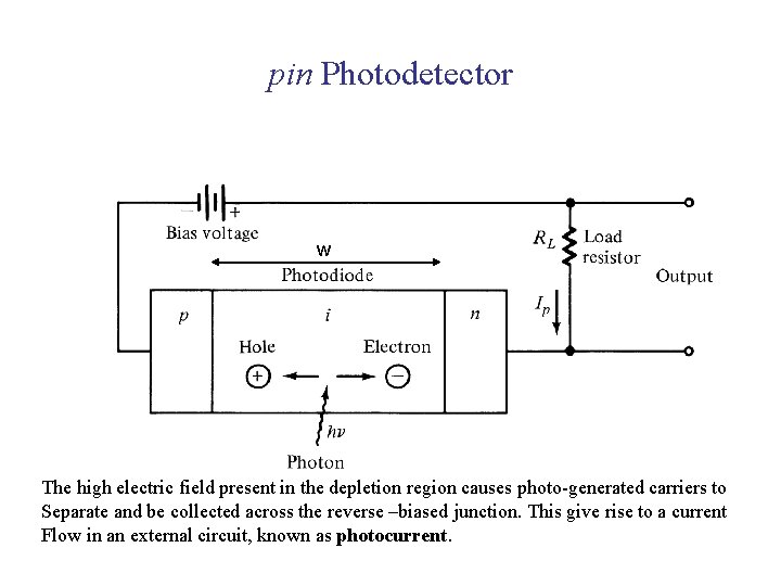
pin Photodetector w The high electric field present in the depletion region causes photo-generated carriers to Separate and be collected across the reverse –biased junction. This give rise to a current Flow in an external circuit, known as photocurrent.

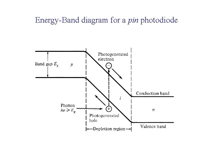
Energy-Band diagram for a pin photodiode

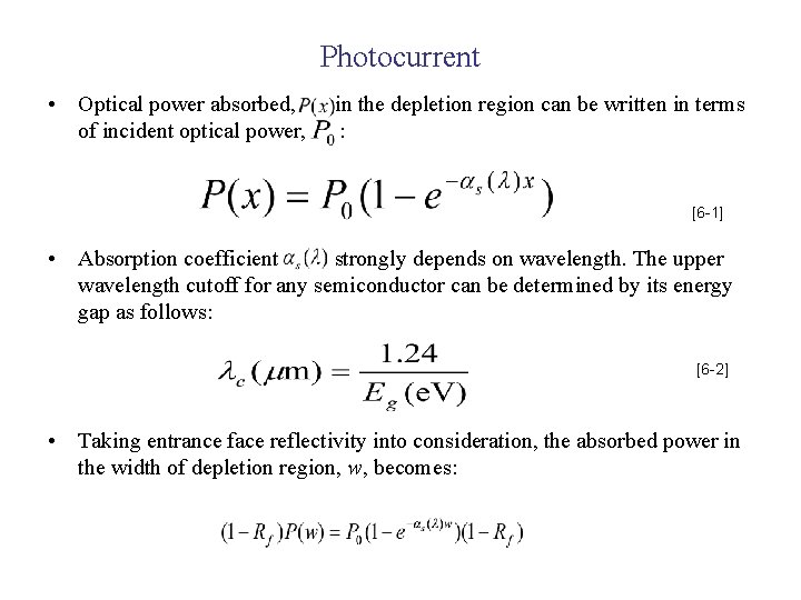
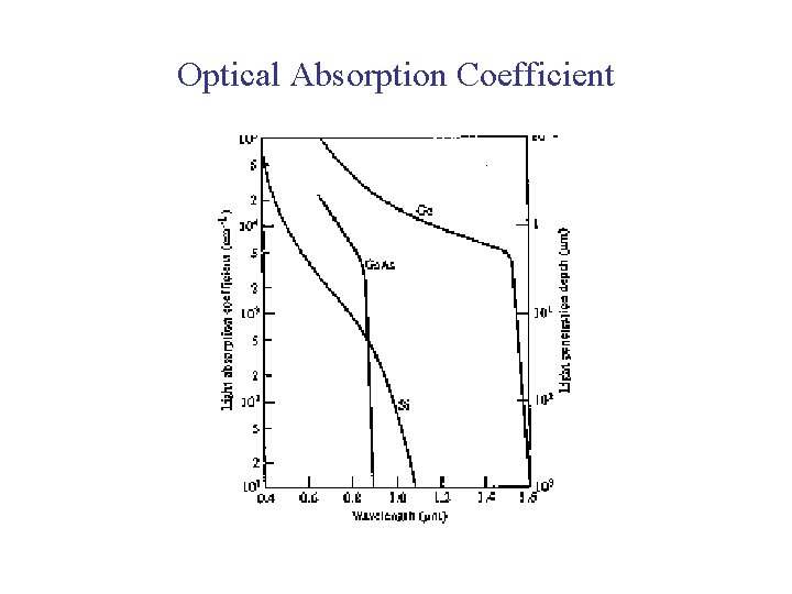
Photocurrent • Optical power absorbed, of incident optical power, in the depletion region can be written in terms : [6 -1] • Absorption coefficient strongly depends on wavelength. The upper wavelength cutoff for any semiconductor can be determined by its energy gap as follows: [6 -2] • Taking entrance face reflectivity into consideration, the absorbed power in the width of depletion region, w, becomes:

Optical Absorption Coefficient
![Responsivity The primary photocurrent resulting from absorption is 6 3 Quantum Efficiency Responsivity • The primary photocurrent resulting from absorption is: [6 -3] • Quantum Efficiency:](https://slidetodoc.com/presentation_image_h/098fa700395b8fb2a060d54b7b23bec8/image-7.jpg)
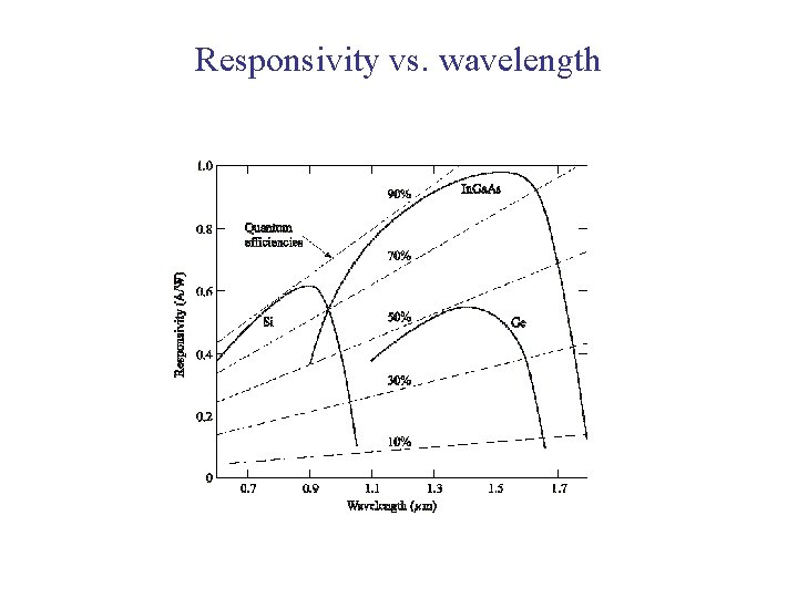
Responsivity • The primary photocurrent resulting from absorption is: [6 -3] • Quantum Efficiency: [6 -4] • Responsivity: [6 -5]

Responsivity vs. wavelength

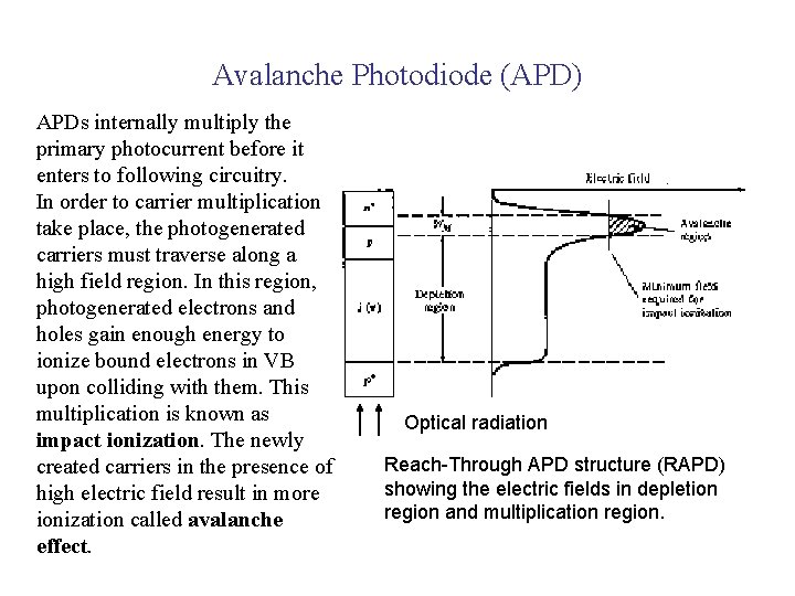
Avalanche Photodiode (APD) APDs internally multiply the primary photocurrent before it enters to following circuitry. In order to carrier multiplication take place, the photogenerated carriers must traverse along a high field region. In this region, photogenerated electrons and holes gain enough energy to ionize bound electrons in VB upon colliding with them. This multiplication is known as impact ionization. The newly created carriers in the presence of high electric field result in more ionization called avalanche effect. Optical radiation Reach-Through APD structure (RAPD) showing the electric fields in depletion region and multiplication region.

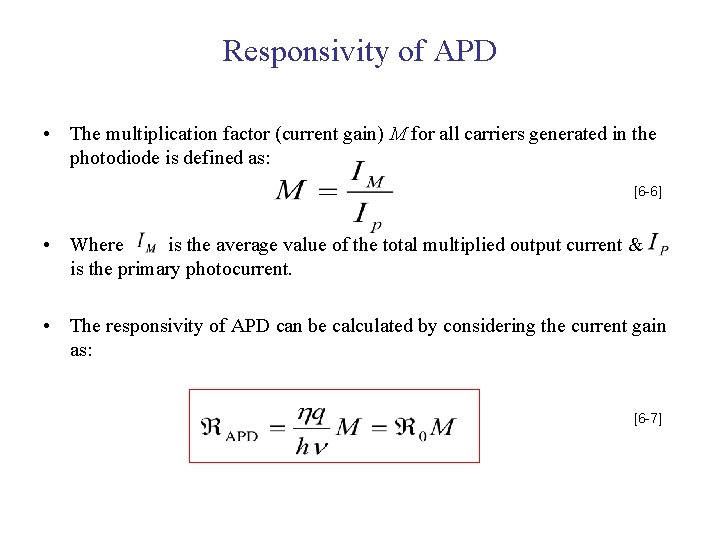
Responsivity of APD • The multiplication factor (current gain) M for all carriers generated in the photodiode is defined as: [6 -6] • Where is the average value of the total multiplied output current & is the primary photocurrent. • The responsivity of APD can be calculated by considering the current gain as: [6 -7]

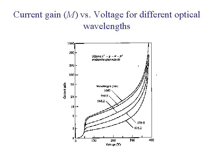
Current gain (M) vs. Voltage for different optical wavelengths

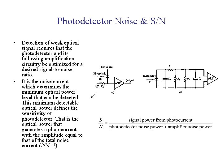
Photodetector Noise & S/N • • Detection of weak optical signal requires that the photodetector and its following amplification circuitry be optimized for a desired signal-to-noise ratio. It is the noise current which determines the minimum optical power level that can be detected. This minimum detectable optical power defines the sensitivity of photodetector. That is the optical power that generates a photocurrent with the amplitude equal to that of the total noise current (S/N=1)

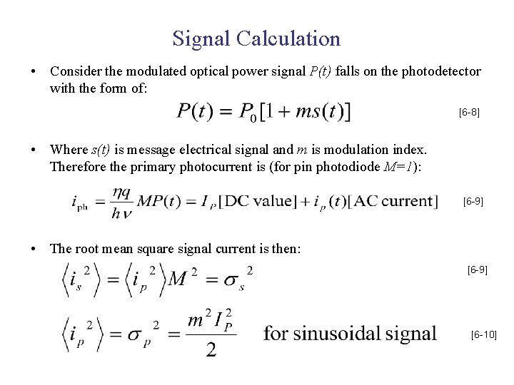
Signal Calculation • Consider the modulated optical power signal P(t) falls on the photodetector with the form of: [6 -8] • Where s(t) is message electrical signal and m is modulation index. Therefore the primary photocurrent is (for pin photodiode M=1): [6 -9] • The root mean square signal current is then: [6 -9] [6 -10]

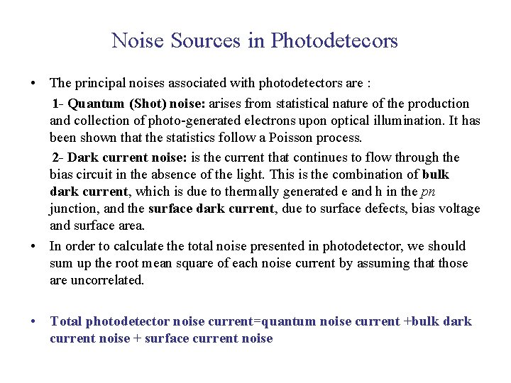
Noise Sources in Photodetecors • The principal noises associated with photodetectors are : 1 - Quantum (Shot) noise: arises from statistical nature of the production and collection of photo-generated electrons upon optical illumination. It has been shown that the statistics follow a Poisson process. 2 - Dark current noise: is the current that continues to flow through the bias circuit in the absence of the light. This is the combination of bulk dark current, which is due to thermally generated e and h in the pn junction, and the surface dark current, due to surface defects, bias voltage and surface area. • In order to calculate the total noise presented in photodetector, we should sum up the root mean square of each noise current by assuming that those are uncorrelated. • Total photodetector noise current=quantum noise current +bulk dark current noise + surface current noise
![Noise calculation 1 Quantum noise current lower limit on the sensitivity 6 11 Noise calculation (1) • Quantum noise current (lower limit on the sensitivity): [6 -11]](https://slidetodoc.com/presentation_image_h/098fa700395b8fb2a060d54b7b23bec8/image-15.jpg)
Noise calculation (1) • Quantum noise current (lower limit on the sensitivity): [6 -11] • B: Bandwidth, F(M) is the noise figure and generally is • Bulk dark current noise: [6 -12] Note that for pin photodiode is bulk dark current • Surface dark current noise: is the surface current. [6 -13]
![Noise calculation 2 The total rms photodetector noise current is 6 14 Noise calculation (2) • The total rms photodetector noise current is: [6 -14] •](https://slidetodoc.com/presentation_image_h/098fa700395b8fb2a060d54b7b23bec8/image-16.jpg)
Noise calculation (2) • The total rms photodetector noise current is: [6 -14] • The thermal noise of amplifier connected to the photodetector is: [6 -15] input resistance of amplifier, and is Boltzmann cte.

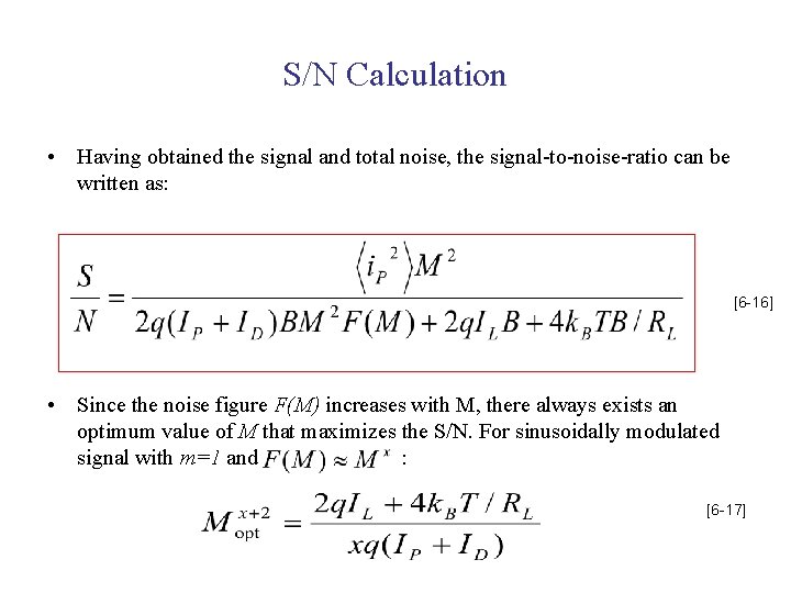
S/N Calculation • Having obtained the signal and total noise, the signal-to-noise-ratio can be written as: [6 -16] • Since the noise figure F(M) increases with M, there always exists an optimum value of M that maximizes the S/N. For sinusoidally modulated signal with m=1 and : [6 -17]

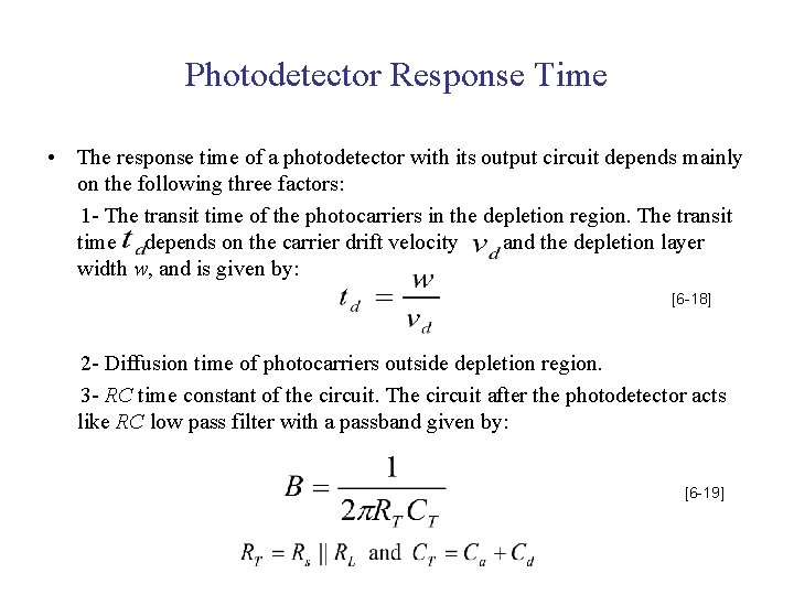
Photodetector Response Time • The response time of a photodetector with its output circuit depends mainly on the following three factors: 1 - The transit time of the photocarriers in the depletion region. The transit time depends on the carrier drift velocity and the depletion layer width w, and is given by: [6 -18] 2 - Diffusion time of photocarriers outside depletion region. 3 - RC time constant of the circuit. The circuit after the photodetector acts like RC low pass filter with a passband given by: [6 -19]

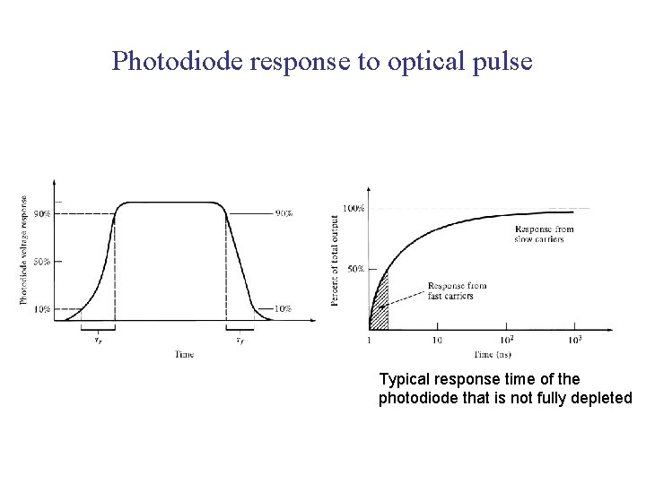
Photodiode response to optical pulse Typical response time of the photodiode that is not fully depleted

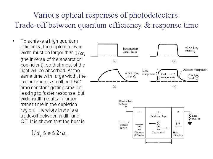
Various optical responses of photodetectors: Trade-off between quantum efficiency & response time • To achieve a high quantum efficiency, the depletion layer width must be larger than (the inverse of the absorption coefficient), so that most of the light will be absorbed. At the same time with large width, the capacitance is small and RC time constant getting smaller, leading to faster response, but wide width results in larger transit time in the depletion region. Therefore there is a trade-off between width and QE. It is shown that the best is:

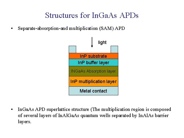
Structures for In. Ga. As APDs • Separate-absorption-and multiplication (SAM) APD light In. P substrate In. P buffer layer INGa. As Absorption layer In. P multiplication layer Metal contact • In. Ga. As APD superlattice structure (The multiplication region is composed of several layers of In. Al. Ga. As quantum wells separated by In. Al. As barrier layers.

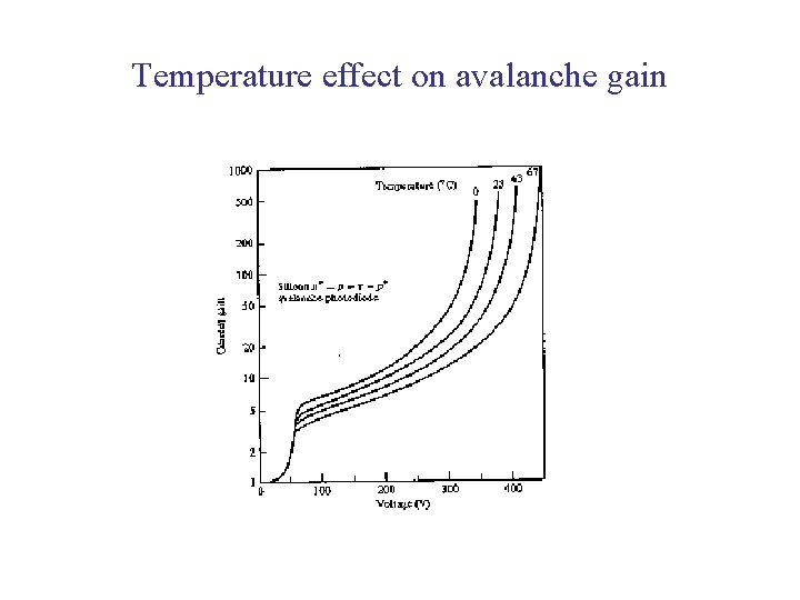
Temperature effect on avalanche gain

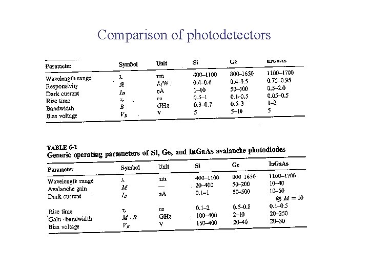
Comparison of photodetectors