Voxtel SPADSi PM ROIC and Multichannel TDC Technologies

- Slides: 28

Voxtel SPAD/Si. PM, ROIC, and Multi-channel TDC Technologies Date: 4/12/2012 Voxtel Contacts: George Williams (georgew@voxtel-inc. com) Vinit Dhulla (vinitd@voxtel-inc. com) Adam Lee (adaml@voxtel-inc. com) Address: 15985 NW Schendel Ave, Suite 200, Beaverton, OR 97006

Presentation Agenda Voxtel Overview Silicon APD Development AQC Based ROIC Development Hybridization Development Other DOE Related ROIC Development Activity Multi-channel, Reconfigurable Pulse-processing Instrumentation

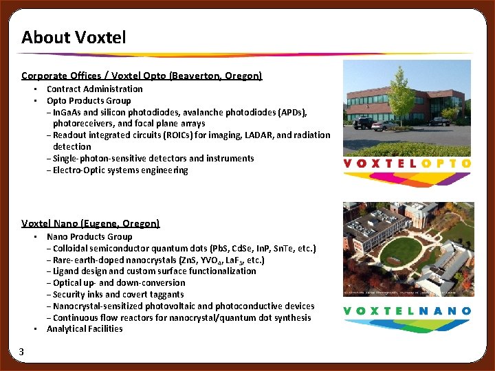
About Voxtel Corporate Offices / Voxtel Opto (Beaverton, Oregon) • Contract Administration • Opto Products Group − In. Ga. As and silicon photodiodes, avalanche photodiodes (APDs), photoreceivers, and focal plane arrays − Readout integrated circuits (ROICs) for imaging, LADAR, and radiation detection − Single-photon-sensitive detectors and instruments − Electro-Optic systems engineering Voxtel Nano (Eugene, Oregon) • Nano Products Group − Colloidal semiconductor quantum dots (Pb. S, Cd. Se, In. P, Sn. Te, etc. ) − Rare-earth-doped nanocrystals (Zn. S, YVO 4, La. F 3, etc. ) − Ligand design and custom surface functionalization − Optical up- and down-conversion − Security inks and covert taggants − Nanocrystal-sensitized photovoltaic and photoconductive devices − Continuous flow reactors for nanocrystal/quantum dot synthesis • Analytical Facilities 3

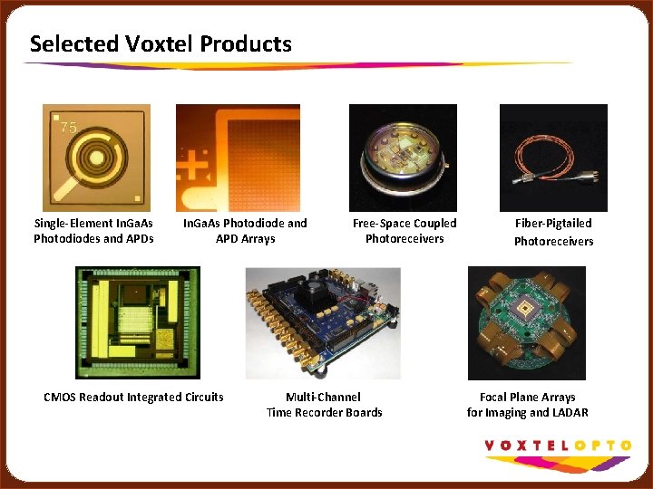
Selected Voxtel Products Single-Element In. Ga. As Photodiodes and APDs In. Ga. As Photodiode and APD Arrays CMOS Readout Integrated Circuits Free-Space Coupled Photoreceivers Multi-Channel Time Recorder Boards Fiber-Pigtailed Photoreceivers Focal Plane Arrays for Imaging and LADAR

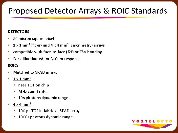
Proposed Detector Arrays & ROIC Standards DETECTORS • 50 micron square pixel • 1 x 1 mm 2 (fiber) and 4 x 4 mm 2 (calorimetry) arrays • compatible with face-to-face (f 2 f) or TSV bonding • Back-illuminated for 300 nm response ROICs: • Matched to SPAD arrays • 1 x 1 mm 2 • nsec TOF on chip • MHz count rates • 10 s photons dynamic range • 4 x 4 mm 2 • 100 ps TOF in fabric of SPAD array • 1000 s photons dynamic range

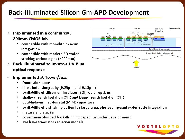
Back-illuminated Silicon Gm-APD Development • Implemented in a commercial, 200 mm CMOS fab • compatible with monolithic circuit integration • compatible with modern 3 D wafer stacking technologies (>200 mm) • Back-illuminated to improve UV-Blue optical response • Implemented at Tower/Jazz • • • Domestic source fine photolithography (0. 25µm and 0. 18µm) availability of silicon-on-insulator (SOI) wafer options shallow Trench Isolation (STI) and Deep Trench Isolation (STI) double-layer metal-metal (Mi. M) capacitors availability of a stitching option for large area, photocomposed wafer-scale integration mature and stabile government-funded back-thinning capabiltiy under development we have transistor radiation models

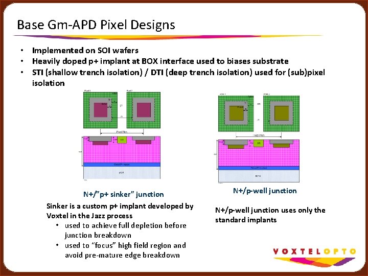
Base Gm-APD Pixel Designs • Implemented on SOI wafers • Heavily doped p+ implant at BOX interface used to biases substrate • STI (shallow trench isolation) / DTI (deep trench isolation) used for (sub)pixel isolation N+/”p+ sinker” junction Sinker is a custom p+ implant developed by Voxtel in the Jazz process • used to achieve full depletion before junction breakdown • used to “focus” high field region and avoid pre-mature edge breakdown N+/p-well junction uses only the standard implants

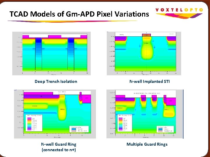
TCAD Models of Gm-APD Pixel Variations Deep Trench Isolation N-well Guard Ring (connected to n+) N-well Implanted STI Multiple Guard Rings

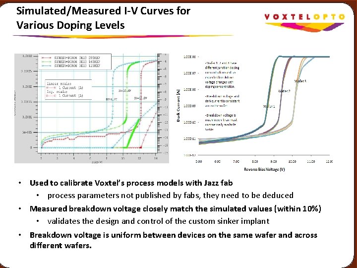
Simulated/Measured I-V Curves for Various Doping Levels • Used to calibrate Voxtel’s process models with Jazz fab • process parameters not published by fabs, they need to be deduced • Measured breakdown voltage closely match the simulated values (within 10%) • validates the design and control of the custom sinker implant • Breakdown voltage is uniform between devices on the same wafer and across different wafers.

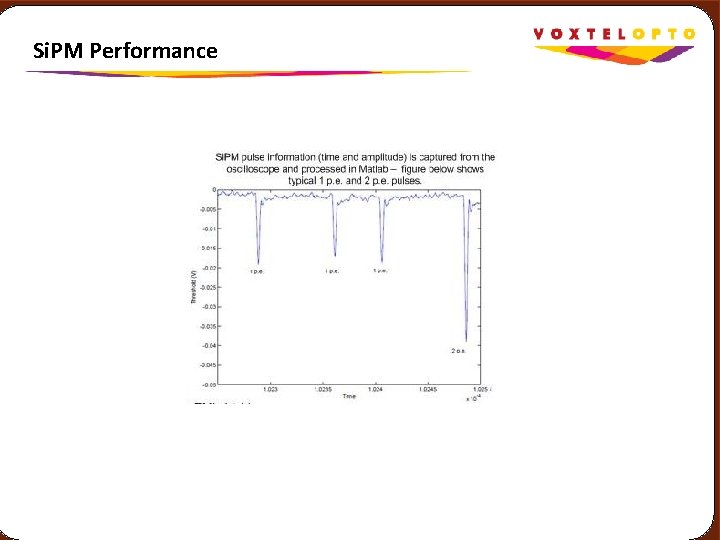
Si. PM Performance

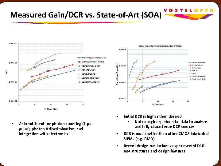
Measured Gain/DCR vs. State-of-Art (SOA) • Gain sufficient for photon counting (1 p. e. pulse), photon # discrimination, and integration with electronics • Initial DCR is higher then desired • Not enough experimental data to analyze and fully characterize DCR sources • DCR is much better than other CMOS fabricated Si. PMs (e. g. RMD) • Recent design run includes experimental DCR test structures and design features

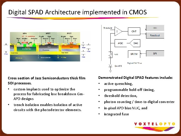
Digital SPAD Architecture implemented in CMOS Cross section of Jazz Semiconductors thick film SOI processes. • custom implants used to optimize the process for fabricating low breakdown Gm. APD designs • trench isolation enables isolation of active circuits with the photodetector elements. Demonstrated Digital SPAD features include: • • • active quenching, programmable hold-off timing, threshold detection, photon counting / time-to-digital converter in-pixel APD bias NUC, and integrated fuse

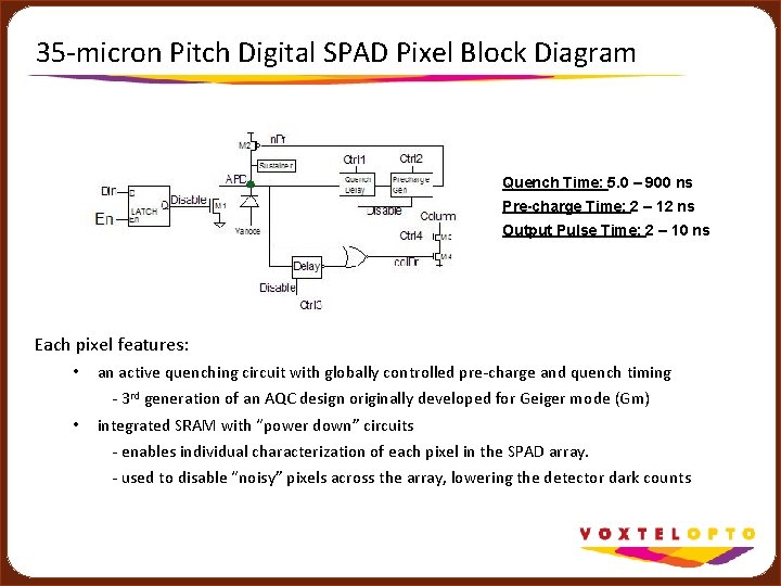
35 -micron Pitch Digital SPAD Pixel Block Diagram Quench Time: 5. 0 – 900 ns Pre-charge Time: 2 – 12 ns Output Pulse Time: 2 – 10 ns Each pixel features: • an active quenching circuit with globally controlled pre-charge and quench timing - 3 rd generation of an AQC design originally developed for Geiger mode (Gm) • integrated SRAM with “power down” circuits - enables individual characterization of each pixel in the SPAD array. - used to disable “noisy” pixels across the array, lowering the detector dark counts

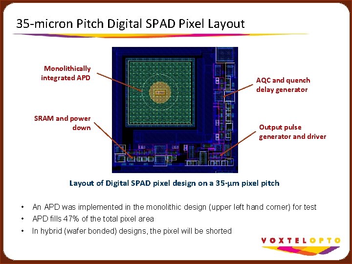
35 -micron Pitch Digital SPAD Pixel Layout Monolithically integrated APD SRAM and power down AQC and quench delay generator Output pulse generator and driver Layout of Digital SPAD pixel design on a 35 -µm pixel pitch • An APD was implemented in the monolithic design (upper left hand corner) for test • APD fills 47% of the total pixel area • In hybrid (wafer bonded) designs, the pixel will be shorted

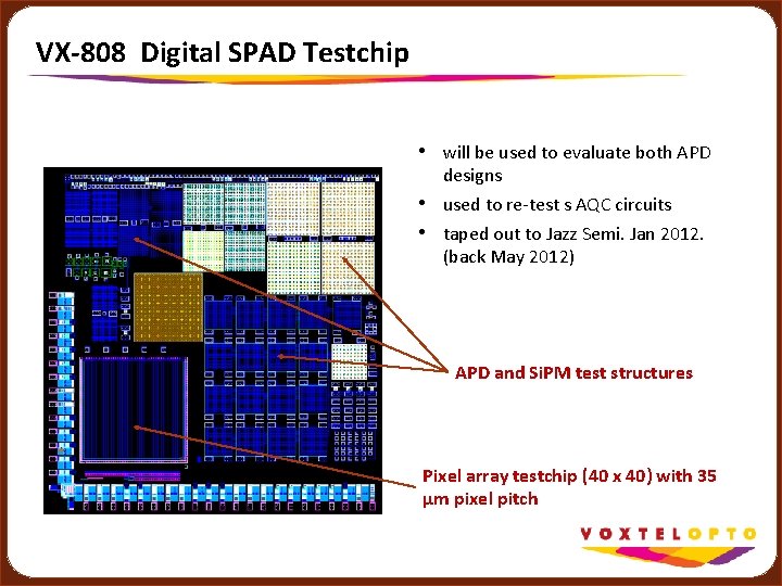
VX-808 Digital SPAD Testchip • will be used to evaluate both APD designs • used to re-test s AQC circuits • taped out to Jazz Semi. Jan 2012. (back May 2012) APD and Si. PM test structures Pixel array testchip (40 x 40) with 35 µm pixel pitch

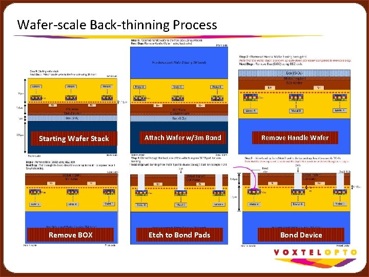
Wafer-scale Back-thinning Process Starting Wafer Stack Remove BOX Attach Wafer w/3 m Bond Etch to Bond Pads Remove Handle Wafer Bond Device

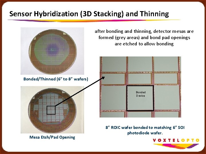
Sensor Hybridization (3 D Stacking) and Thinning after bonding and thinning, detector mesas are formed (grey areas) and bond pad openings are etched to allow bonding Bonded/Thinned (6” to 8” wafers) Bonded Device Mesa Etch/Pad Opening 8” ROIC wafer bonded to matching 6” SOI photodiode wafer.

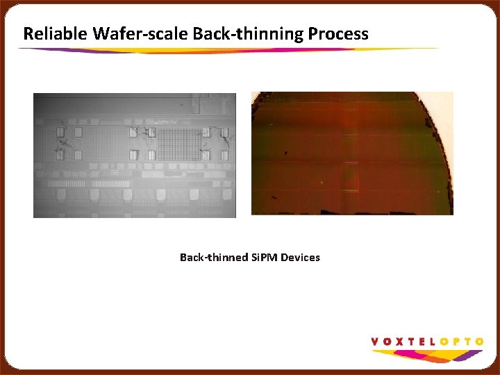
Reliable Wafer-scale Back-thinning Process Back-thinned Si. PM Devices

Voxtel SPAD/Si. PM Phase II SBIR Efforts Under Review Topic 61: Wafer-Scale Geiger-mode Silicon Photomultiplier Arrays Fabricated Using Domestic CMOS Fab Characterize latest generation of Gm APDs fabricated in Phase I Optimize a low DCR Gm SPAD (Si. PM) using Jazz process Assumes a 25 -µm pixel pitch Optimized for backside illumination Compatible with large area stitching, but included in program Topic 63 a: Digital Silicon Photomultiplier Array Readout Integrated Circuits Characterize digital SPAD ROIC fabricated at Jazz in Phase I Develop a 25 micron pitch ROIC for digital SPADS Designed for hybrid stacked circuit of bump bond integration Design includes: In-pixel AQC In-pixel (sub)pixel enable (Optional) monolithic Gm SPAD, which can be shorted for 3 D stacked integration* Sub-block asynchronous TDC Programmable threshold

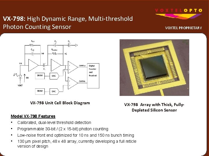
VX-798: High Dynamic Range, Multi-threshold Photon Counting Sensor VX-798 Unit Cell Block Diagram VX-798 Array with Thick, Fully. Depleted Silicon Sensor Model VX-798 Features • • VOXTEL PROPRIETARY Calibrated, dual-level threshold detection Programmable 30 -bit / (2 x 15 -bit) photon counting Low-noise front end optimized for 10 ns and 150 ns bunch timing 130 µm pixel pitch, 48 x 48 array, currently developing a full reticle version of design

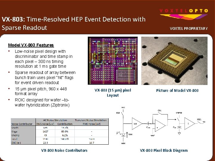
VX-803: Time-Resolved HEP Event Detection with Sparse Readout Model VX-803 Features • Low-noise pixel design with discriminator and time stamp in each pixel – 300 ns timing resolution at 1 ms gate time • Sparse readout of array between bunch train uses pixel “hit” flags for event driven readout • 15 µm pixel pitch, 960 x 448 format array • ROIC designed for wafer –towafer hybridization (Ziptronix) VX-803 Noise Contributors VX-803 (15 µm) pixel Layout VOXTEL PROPRIETARY Picture of Model VX-803 Pixel Block Diagram

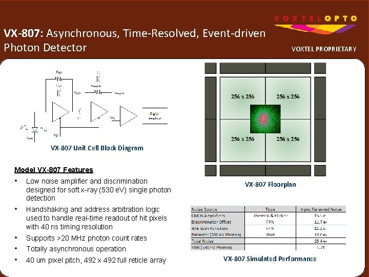
VX-807: Asynchronous, Time-Resolved, Event-driven Photon Detector VOXTEL PROPRIETARY VX-807 Unit Cell Block Diagram Model VX-807 Features • Low noise amplifier and discrimination designed for soft x-ray (530 e. V) single photon detection • Handshaking and address arbitration logic used to handle real-time readout of hit pixels with 40 ns timing resolution • • • Supports >20 MHz photon count rates VX-807 Floorplan Totally asynchronous operation 40 um pixel pitch, 492 x 492 full reticle array VX-807 Simulated Performance

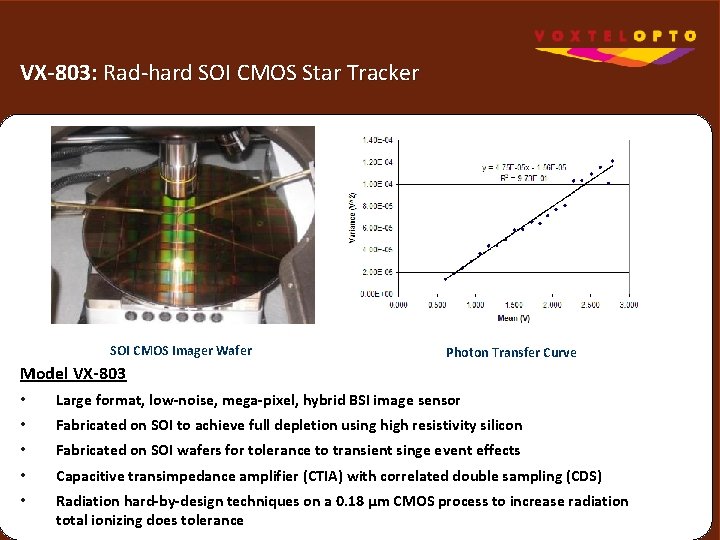
VX-803: R VX-803: ad-hard SOI CMOS Star Tracker SOI CMOS Imager Wafer Photon Transfer Curve Model VX-803 • Large format, low-noise, mega-pixel, hybrid BSI image sensor • Fabricated on SOI to achieve full depletion using high resistivity silicon • Fabricated on SOI wafers for tolerance to transient singe event effects • Capacitive transimpedance amplifier (CTIA) with correlated double sampling (CDS) • Radiation hard-by-design techniques on a 0. 18 µm CMOS process to increase radiation total ionizing does tolerance

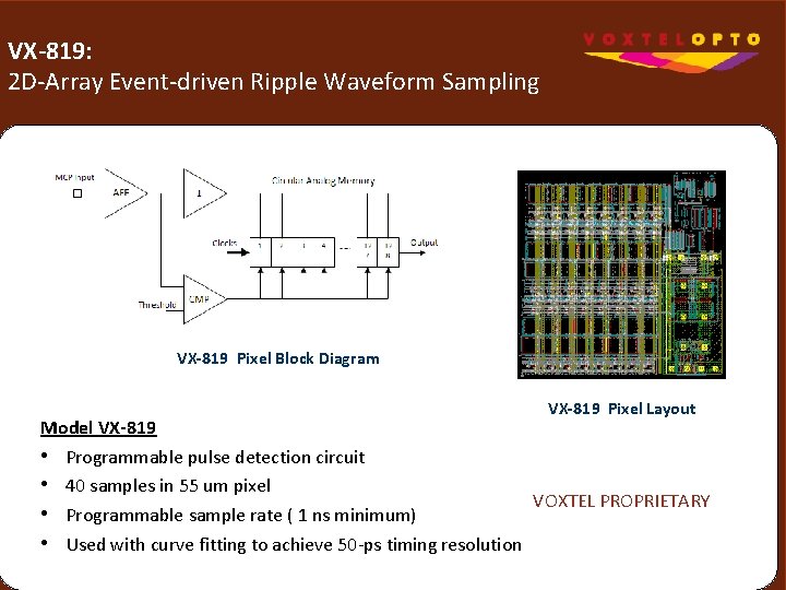
VX-819: 2 D-Array Event-driven Ripple Waveform Sampling VX-819 Pixel Block Diagram VX-819 Pixel Layout Model VX-819 • Programmable pulse detection circuit • 40 samples in 55 um pixel VOXTEL PROPRIETARY • Programmable sample rate ( 1 ns minimum) • Used with curve fitting to achieve 50 -ps timing resolution

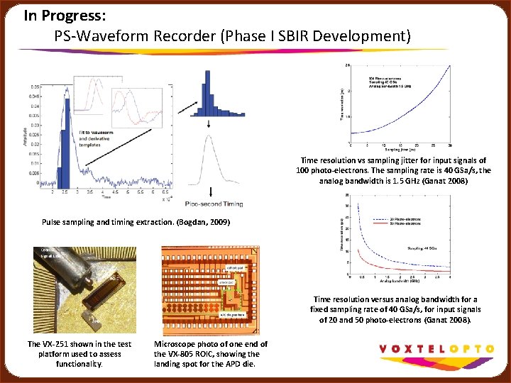
In Progress: PS-Waveform Recorder (Phase I SBIR Development) Time resolution vs sampling jitter for input signals of 100 photo-electrons. The sampling rate is 40 GSa/s, the analog bandwidth is 1. 5 GHz (Ganat 2008) Pulse sampling and timing extraction. (Bogdan, 2009) Time resolution versus analog bandwidth for a fixed sampling rate of 40 GSa/s, for input signals of 20 and 50 photo-electrons (Ganat 2008). The VX-251 shown in the test platform used to assess functionality. Microscope photo of one end of the VX-805 ROIC, showing the landing spot for the APD die.

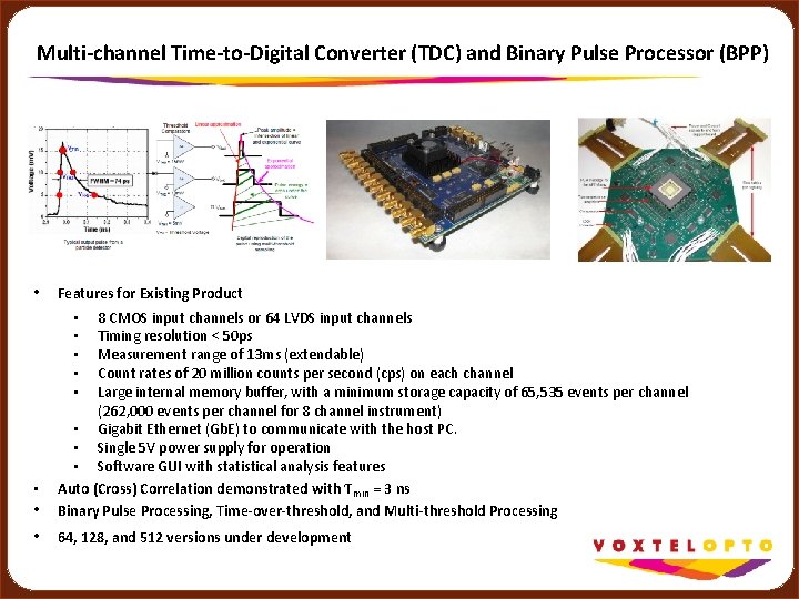
Multi-channel Time-to-Digital Converter (TDC) and Binary Pulse Processor (BPP) • Features for Existing Product • 8 CMOS input channels or 64 LVDS input channels Timing resolution < 50 ps Measurement range of 13 ms (extendable) Count rates of 20 million counts per second (cps) on each channel Large internal memory buffer, with a minimum storage capacity of 65, 535 events per channel (262, 000 events per channel for 8 channel instrument) • Gigabit Ethernet (Gb. E) to communicate with the host PC. • Single 5 V power supply for operation • Software GUI with statistical analysis features Auto (Cross) Correlation demonstrated with Ƭmin = 3 ns Binary Pulse Processing, Time-over-threshold, and Multi-threshold Processing • 64, 128, and 512 versions under development • • •

High channel Count, Re-configurable Multi-Purpose Pulseprocessing Platform Planned Features • Easily reconfigurable pulse-processing platform with multiple daughter boards to meet different application needs • Application-specific, pluggable front-end modules – time-stamping (analog and digital inputs), analog to digital conversion, auto and cross-correlation • Up to 1000 channels • High timing resolution (tens of pico-seconds to sub-ns, depending on the channel count and application) • Data transfer rates of up to 400 MB/s • Variable measurement times, depending on the application • Ability to time-stamp positive and negative edges • Ability to measure really short pulses (<1 ns) • Minimum dead-time between pulses (<3 ns) • High input pulse count rates (> 250 MHz) • User friendly software GUI

Thank You