pico TDC Picosecond TDC for HEP Moritz Horstmann

- Slides: 29


pico. TDC: Pico-second TDC for HEP Moritz Horstmann, Jorgen Christiansen, Bram Faes (KU Leuven), Lukas Perktold (Now AMS), Jeffrey Prinzie (KU Leuven) CERN/EP-ESE

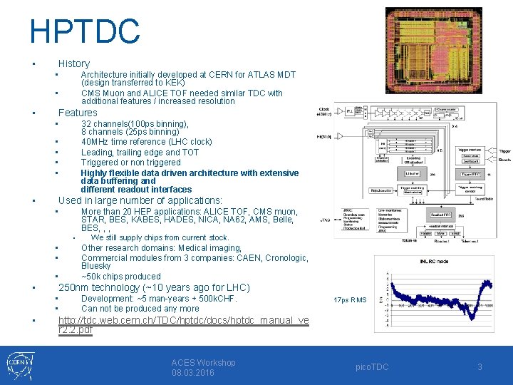
HPTDC • History Architecture initially developed at CERN for ATLAS MDT (design transferred to KEK) CMS Muon and ALICE TOF needed similar TDC with additional features / increased resolution • • • Features 32 channels(100 ps binning), 8 channels (25 ps binning) 40 MHz time reference (LHC clock) Leading, trailing edge and TOT Triggered or non triggered Highly flexible data driven architecture with extensive data buffering and different readout interfaces • • • Used in large number of applications: More than 20 HEP applications: ALICE TOF, CMS muon, STAR, BES, KABES, HADES, NICA, NA 62, AMS, Belle, BES, , , • • • 250 nm technology (~10 years ago for LHC) • • • We still supply chips from current stock. Other research domains: Medical imaging, Commercial modules from 3 companies: CAEN, Cronologic, Bluesky ~50 k chips produced Development: ~5 man-years + 500 k. CHF. Can not be produced any more 17 ps RMS http: //tdc. web. cern. ch/TDC/hptdc/docs/hptdc_manual_ve r 2. 2. pdf ACES Workshop 08. 03. 2016 pico. TDC 3

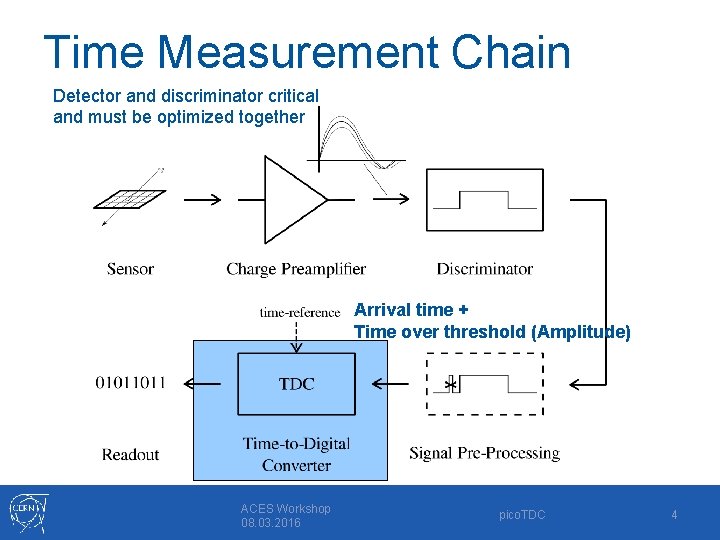
Time Measurement Chain Detector and discriminator critical and must be optimized together Arrival time + Time over threshold (Amplitude) ACES Workshop 08. 03. 2016 pico. TDC 4

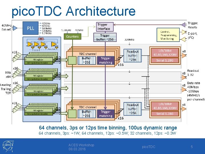
pico. TDC Architecture 64 channels, 3 ps or 12 ps time binning, 100 us dynamic range 64 channels, 3 ps: ~1 W; 64 channels, 12 ps: ~0. 5 W; 32 channels, 12 ps: ~0. 3 W ACES Workshop 08. 03. 2016 pico. TDC 5

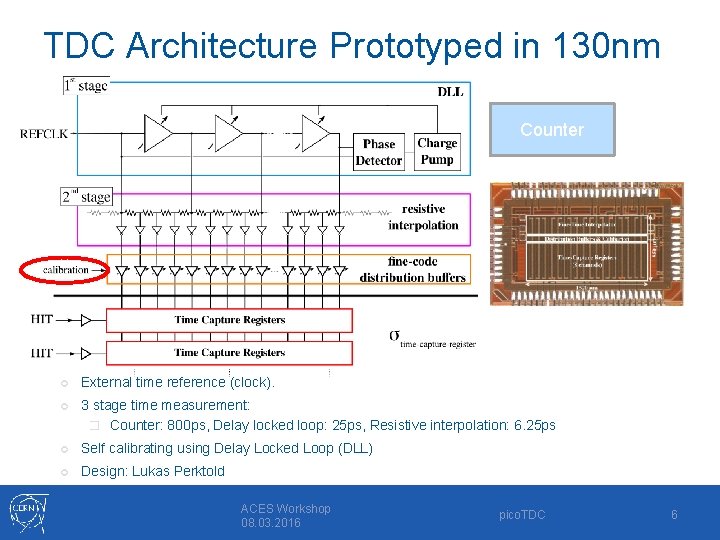
TDC Architecture Prototyped in 130 nm Counter External time reference (clock). 3 stage time measurement: � Counter: 800 ps, Delay locked loop: 25 ps, Resistive interpolation: 6. 25 ps Self calibrating using Delay Locked Loop (DLL) Design: Lukas Perktold ACES Workshop 08. 03. 2016 pico. TDC 6

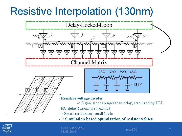
Resistive Interpolation (130 nm) Resistive voltage divider -> Signal slopes longer than delay, stabilized by DLL ● RC delay (capacitive loading) - > Small resistances, small loads ● - > Simulation based optimization of resistor values ACES Workshop 08. 03. 2016 pico. TDC 7

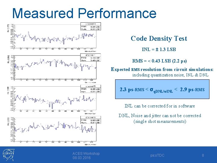
Measured Performance Code Density Test INL = ± 1. 3 LSB RMS = < 0. 43 LSB (2. 2 ps) Expected RMS resolution from circuit simulations: including quantization noise, INL & DNL 2. 3 ps-RMS < σq. DNL/w. INL < 2. 9 ps-RMS INL can be corrected for in software DNL, Noise and jitter can not be corrected (single shot measurements) ACES Workshop 08. 03. 2016 pico. TDC 8

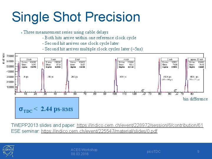
Single Shot Precision ● Three measurement series using cable delays - Both hits arrive within one reference clock cycle - Second hit arrives one clock cycle later - Second hit arrives multiple clock cycles later (~5 ns) bin difference σTDC < 2. 44 ps-RMS TWEPP 2013 slides and paper: https: //indico. cern. ch/event/228972/session/6/contribution/61 ESE seminar: https: //indico. cern. ch/event/225547/material/slides/0. pdf ACES Workshop 08. 03. 2016 pico. TDC 9

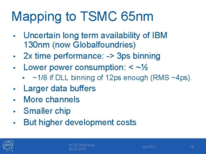
Mapping to TSMC 65 nm Uncertain long term availability of IBM 130 nm (now Globalfoundries) • 2 x time performance: -> 3 ps binning • Lower power consumption: < ~½ • • ~1/8 if DLL binning of 12 ps enough (RMS ~4 ps). Larger data buffers • More channels • Smaller chip • But higher development costs • ACES Workshop 08. 03. 2016 pico. TDC 10

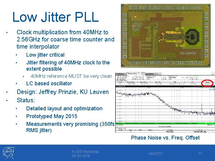
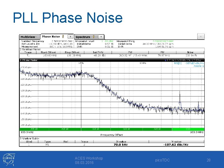
Low Jitter PLL • Clock multiplication from 40 MHz to 2. 56 GHz for coarse time counter and time interpolator Low jitter critical Jitter filtering of 40 MHz clock to the extent possible • • • 40 MHz reference MUST be very clean LC based oscillator Design: Jeffrey Prinzie, KU Leuven Status: • • • Detailed layout and optimization Prototyped May 2015 Measurements very promising (350 fs RMS jitter) Phase Noise vs. Freq. Offset ACES Workshop 08. 03. 2016 pico. TDC 11

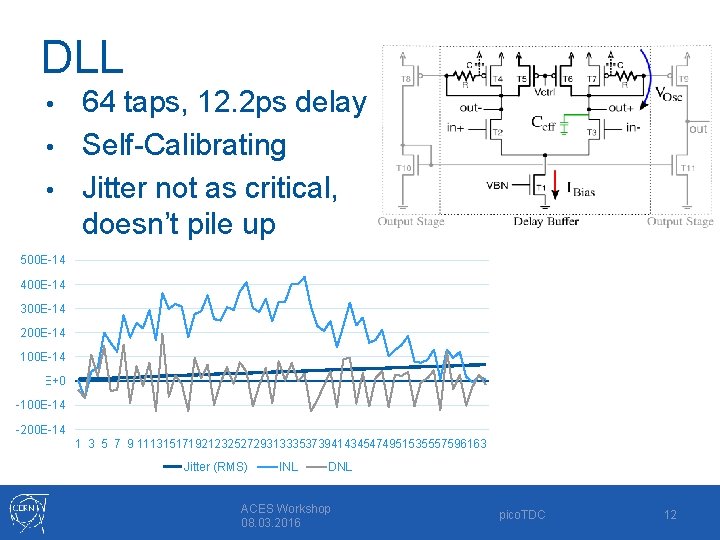
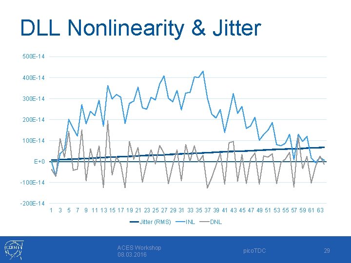
DLL 64 taps, 12. 2 ps delay • Self-Calibrating • Jitter not as critical, doesn’t pile up • 500 E-14 400 E-14 300 E-14 200 E-14 100 E-14 000 E+0 -100 E-14 -200 E-14 1 3 5 7 9 111315171921232527293133353739414345474951535557596163 Jitter (RMS) INL DNL ACES Workshop 08. 03. 2016 pico. TDC 12

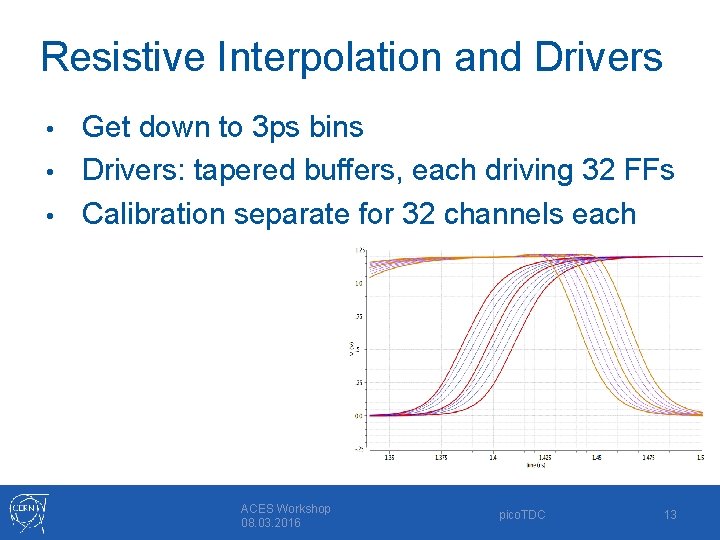
Resistive Interpolation and Drivers Get down to 3 ps bins • Drivers: tapered buffers, each driving 32 FFs • Calibration separate for 32 channels each • ACES Workshop 08. 03. 2016 pico. TDC 13

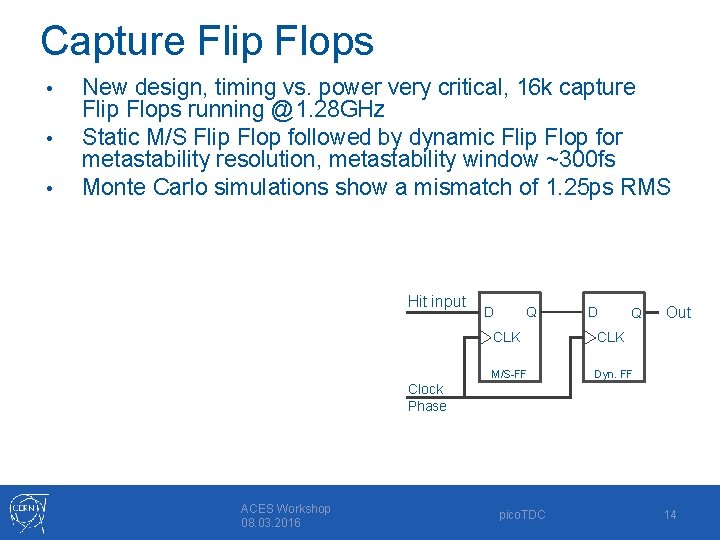
Capture Flip Flops • • • New design, timing vs. power very critical, 16 k capture Flip Flops running @1. 28 GHz Static M/S Flip Flop followed by dynamic Flip Flop for metastability resolution, metastability window ~300 fs Monte Carlo simulations show a mismatch of 1. 25 ps RMS Hit input D Q CLK M/S-FF Dyn. FF Out Clock Phase ACES Workshop 08. 03. 2016 pico. TDC 14

Full Timing Macro • 64 channels, DLL and resistive interpolator in the center • Hit signal input on the left, output on the right ACES Workshop 08. 03. 2016 pico. TDC 15

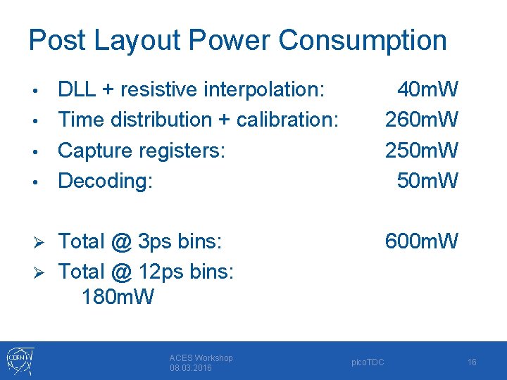
Post Layout Power Consumption • DLL + resistive interpolation: • Time distribution + calibration: • Capture registers: • Decoding: 40 m. W 260 m. W 250 m. W Total @ 3 ps bins: Ø Total @ 12 ps bins: 180 m. W 600 m. W Ø ACES Workshop 08. 03. 2016 pico. TDC 16

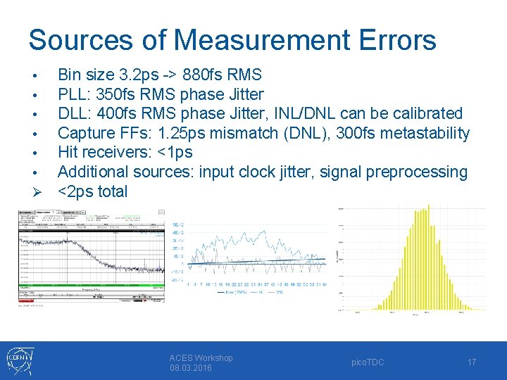
Sources of Measurement Errors • • • Ø Bin size 3. 2 ps -> 880 fs RMS PLL: 350 fs RMS phase Jitter DLL: 400 fs RMS phase Jitter, INL/DNL can be calibrated Capture FFs: 1. 25 ps mismatch (DNL), 300 fs metastability Hit receivers: <1 ps Additional sources: input clock jitter, signal preprocessing <2 ps total ACES Workshop 08. 03. 2016 pico. TDC 17

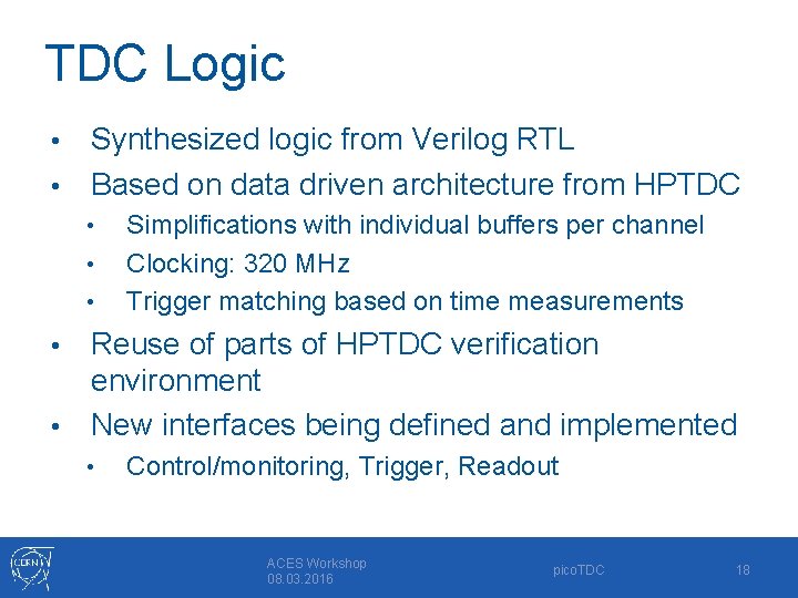
TDC Logic Synthesized logic from Verilog RTL • Based on data driven architecture from HPTDC • • Simplifications with individual buffers per channel Clocking: 320 MHz Trigger matching based on time measurements Reuse of parts of HPTDC verification environment • New interfaces being defined and implemented • • Control/monitoring, Trigger, Readout ACES Workshop 08. 03. 2016 pico. TDC 18

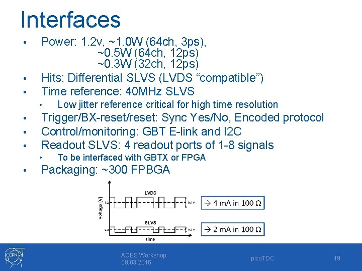
Interfaces • • • Power: 1. 2 v, ~1. 0 W (64 ch, 3 ps), ~0. 5 W (64 ch, 12 ps) ~0. 3 W (32 ch, 12 ps) Hits: Differential SLVS (LVDS “compatible”) Time reference: 40 MHz SLVS • • Trigger/BX-reset/reset: Sync Yes/No, Encoded protocol Control/monitoring: GBT E-link and I 2 C Readout SLVS: 4 readout ports of 1 -8 signals • • Low jitter reference critical for high time resolution To be interfaced with GBTX or FPGA Packaging: ~300 FPBGA ACES Workshop 08. 03. 2016 pico. TDC 19

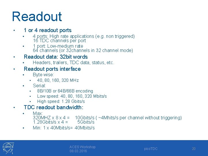
Readout • 1 or 4 readout ports 4 ports: High rate applications (e. g. non triggered) 16 TDC channels per port 1 port: Low-medium rate 64 channels (or 32 channels in 32 channel mode) • • • Readout data: 32 bit words Headers, trailers, TDC data, status, etc. • • Readout ports interface Byte wise: • • Serial: • • • 40, 80, 160, 320 MHz 8 B/10 B or 64 B/66 B encoding Low speed: 40, 80, 160, 320 Mbits/s High speed: 1. 28 Gbits/s TDC readout bandwidth: • • Max: 320 MHZ x 8 x 4 = 10 Gbits/s ( ~4 Mhits/s per channel without triggering) 1. 28 Gbits/s x 4 = 5 Gbits/s Min: 1 x 40 Mbits/s= 40 Mbits/s ACES Workshop 08. 03. 2016 pico. TDC 20

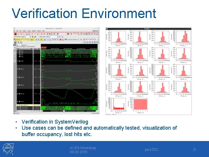
Verification Environment • Verification in System. Verilog • Use cases can be defined and automatically tested, visualization of buffer occupancy, lost hits etc. ACES Workshop 08. 03. 2016 pico. TDC 21

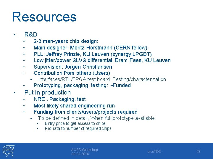
Resources • R&D 2 -3 man-years chip design: Main designer: Moritz Horstmann (CERN fellow) PLL: Jeffrey Prinzie, KU Leuven (synergy LPGBT) Low jitter/power SLVS differential: Bram Faes, KU Leuven Supervision: Jorgen Christiansen Contribution from others (Users) • • Prototyping, packaging, testing: ~Funded • • Interfaces/RTL/FPGA test board: Testing/characterization Put in production NRE , Packaging, test Most likely shared engineering run Funding from clients/users/projects required • • To be defined in detail, When full prototype available. • • Entry price to get access to chips Pro-rata to number of required chips ACES Workshop 08. 03. 2016 pico. TDC 22

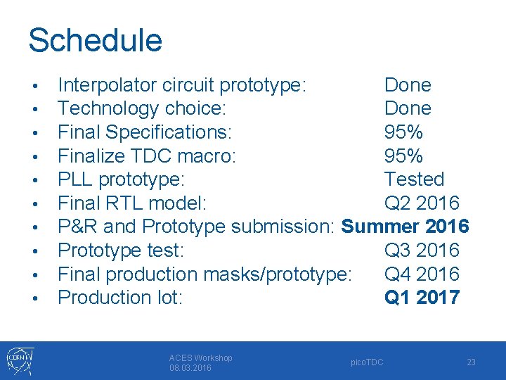
Schedule • • • Interpolator circuit prototype: Done Technology choice: Done Final Specifications: 95% Finalize TDC macro: 95% PLL prototype: Tested Final RTL model: Q 2 2016 P&R and Prototype submission: Summer 2016 Prototype test: Q 3 2016 Final production masks/prototype: Q 4 2016 Production lot: Q 1 2017 ACES Workshop 08. 03. 2016 pico. TDC 23


Backup Slides ACES Workshop 08. 03. 2016 pico. TDC 25

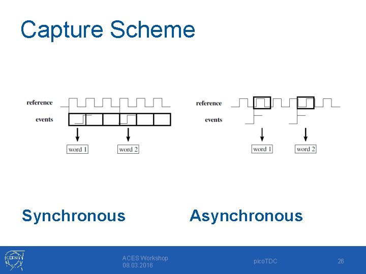
Capture Scheme Synchronous ACES Workshop 08. 03. 2016 Asynchronous pico. TDC 26

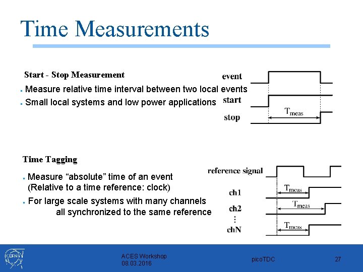
Time Measurements Start - Stop Measurement Measure relative time interval between two local events ● Small local systems and low power applications ● Time Tagging Measure “absolute” time of an event (Relative to a time reference: clock) ● For large scale systems with many channels all synchronized to the same reference ● ACES Workshop 08. 03. 2016 pico. TDC 27

PLL Phase Noise ACES Workshop 08. 03. 2016 pico. TDC 28

DLL Nonlinearity & Jitter 500 E-14 400 E-14 300 E-14 200 E-14 100 E-14 000 E+0 -100 E-14 -200 E-14 1 3 5 7 9 11 13 15 17 19 21 23 25 27 29 31 33 35 37 39 41 43 45 47 49 51 53 55 57 59 61 63 Jitter (RMS) ACES Workshop 08. 03. 2016 INL DNL pico. TDC 29