
Avalanche Photodiodes for 3 D LADAR and Communications



- Slides: 29
Avalanche Photodiodes for 3 -D LADAR and Communications* S. Verghese *This work was sponsored by the National Aeronautics and Space Administration (NASA) Goddard under the Department of the Air Force contract number FA 8721 -05 -C-0002. Opinions, interpretations, conclusions, and recommendations are those of the authors and are not necessarily endorsed by the United States Government. MIT Lincoln Laboratory Verghese_AFRL 101906 -1 S. Verghese 10/19/06
Key Technical Contributors • In. P APDs K. A. Mc. Intosh G. M. Smith K. E. Jensen J. M. Mahan F. J. O’Donnell T. J. Mc. Iver L. Retherford • E. K. Duerr P. I. Hopman J. Aversa C. D. Parker E. A. Dauler J. E. Funk D. Chapman D. C. Oakley C. Vineis S. H. Groves A. Napoleone K. Carbonari S. A. Hamilton D. C. Shaver D. M. Cohen B. F. Aull J. P. Frechette C. N. Stevenson M. Renzi S. Verghese CMOS ROIC E. J. Ouellette J. B. Glettler Verghese_AFRL 101906 -2 S. Verghese 10/19/06 J. P. Donnelly L. J. Mahoney K. M. Molvar Z. -L. Liau M. P. Kesler P. Chapnik G. Lambert MIT Lincoln Laboratory
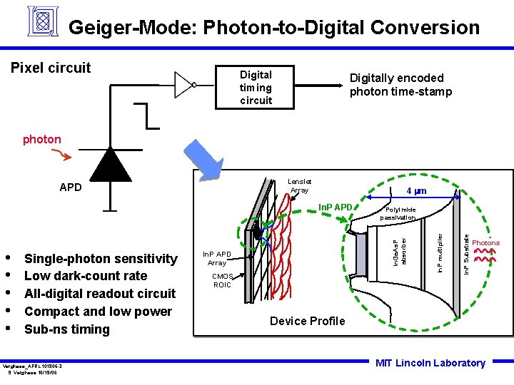
Geiger-Mode: Photon-to-Digital Conversion Pixel circuit Digital timing circuit Digitally encoded photon time-stamp photon Lenslet Array 4 mm Single-photon sensitivity Low dark-count rate All-digital readout circuit Compact and low power Sub-ns timing Verghese_AFRL 101906 -3 S. Verghese 10/19/06 In. P APD Array CMOS ROIC In. P Substrate • • • Polyimide passivation In. Ga. As. P absorber In. P APD In. P multiplier APD Photons Device Profile MIT Lincoln Laboratory
In. P Avalanche Photodiodes Verghese_AFRL 101906 -4 S. Verghese 10/19/06 • Introduction • Applications • APD Figures of Merit • Read-Out Integrated Circuit (ROIC) • Summary MIT Lincoln Laboratory
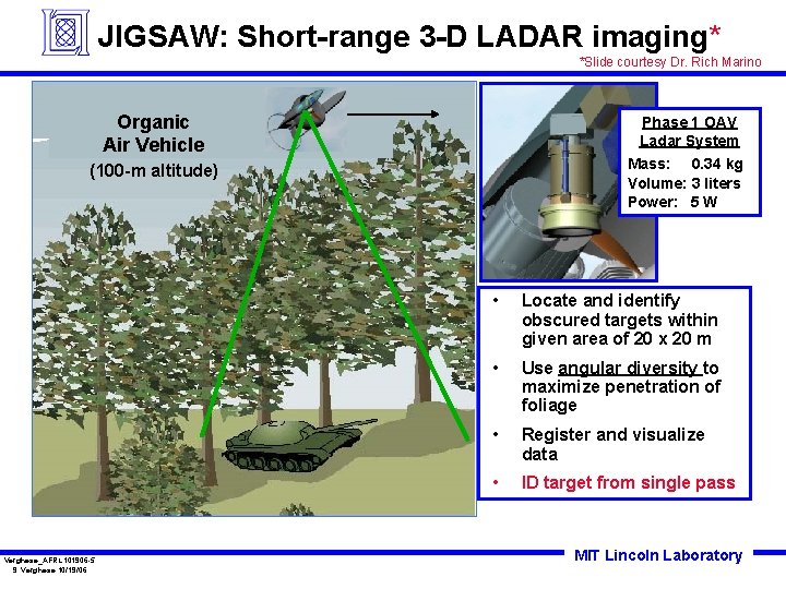
JIGSAW: Short-range 3 -D LADAR imaging* *Slide courtesy Dr. Rich Marino Organic Air Vehicle Phase 1 OAV Ladar System Mass: 0. 34 kg Volume: 3 liters Power: 5 W (100 -m altitude) Verghese_AFRL 101906 -5 S. Verghese 10/19/06 • Locate and identify obscured targets within given area of 20 x 20 m • Use angular diversity to maximize penetration of foliage • Register and visualize data • ID target from single pass MIT Lincoln Laboratory
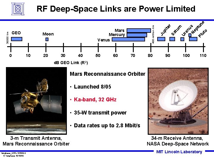
0 10 20 30 40 50 60 70 80 90 ne an u N s ep tu Ur rn tu r Sa ite Mars Mercury Venus Moon Ju p GEO 400 million km 36000 km RF Deep-Space Links are Power Limited 100 u Pl to 110 d. B GEO Link (R 2) Mars Reconnaissance Orbiter • Launched 8/05 • Ka-band, 32 GHz • 35 -W transmit power • Data rates up to 2. 8 Mbit/s 3 -m Transmit Antenna, Mars Reconnaissance Orbiter Verghese_AFRL 101906 -6 S. Verghese 10/19/06 34 -m Receive Antenna, NASA Deep-Space Network MIT Lincoln Laboratory
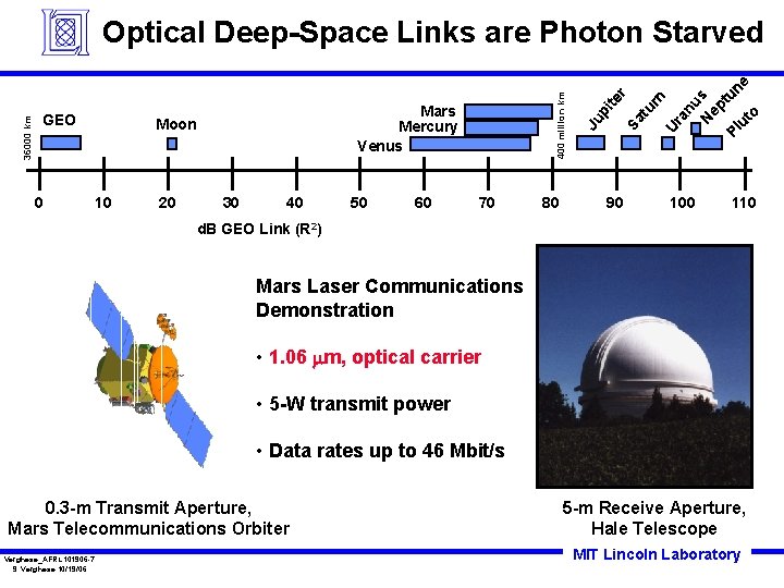
0 10 20 30 40 50 60 70 80 90 ne an u N s ep tu Ur rn tu r Sa ite Mars Mercury Venus Moon Ju p GEO 400 million km 36000 km Optical Deep-Space Links are Photon Starved 100 u Pl 110 d. B GEO Link (R 2) Mars Laser Communications Demonstration • 1. 06 mm, optical carrier • 5 -W transmit power • Data rates up to 46 Mbit/s 0. 3 -m Transmit Aperture, Mars Telecommunications Orbiter Verghese_AFRL 101906 -7 S. Verghese 10/19/06 to 5 -m Receive Aperture, Hale Telescope MIT Lincoln Laboratory
In. P Avalanche Photodiodes • • • Introduction Applications APD Figures of Merit – Photon Detection Efficiency (PDE) – Reset Time – Dark Count Rate (DCR) • • Verghese_AFRL 101906 -8 S. Verghese 10/19/06 Read-Out Integrated Circuit (ROIC) Summary MIT Lincoln Laboratory
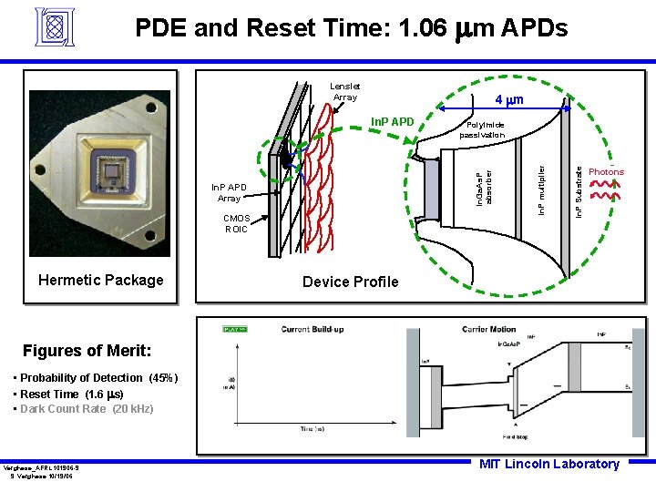
PDE and Reset Time: 1. 06 mm APDs Lenslet Array 4 mm In. P Substrate CMOS ROIC In. P multiplier In. P APD Array Hermetic Package Polyimide passivation In. Ga. As. P absorber In. P APD Photons Device Profile Figures of Merit: • Probability of Detection (45%) • Reset Time (1. 6 ms) • Dark Count Rate (20 k. Hz) Verghese_AFRL 101906 -9 S. Verghese 10/19/06 MIT Lincoln Laboratory
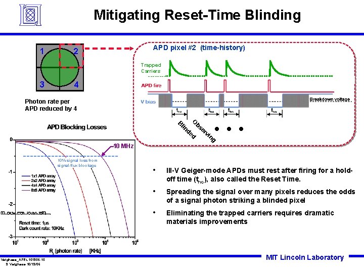
Mitigating Reset-Time Blinding 2 x 2 1 Array APD pixel #2 (time-history) 2 Trapped Carriers 3 4 Photon rate per APD reduced by 4 O B d de lin bs er v in g 10 MHz 10% signal loss from signal-flux blockage Verghese_AFRL 101906 -10 S. Verghese 10/19/06 • III-V Geiger-mode APDs must rest after firing for a holdoff time (tho), also called the Reset Time. • Spreading the signal over many pixels reduces the odds of a signal photon striking a blinded pixel • Eliminating the trapped carriers requires dramatic materials improvements MIT Lincoln Laboratory
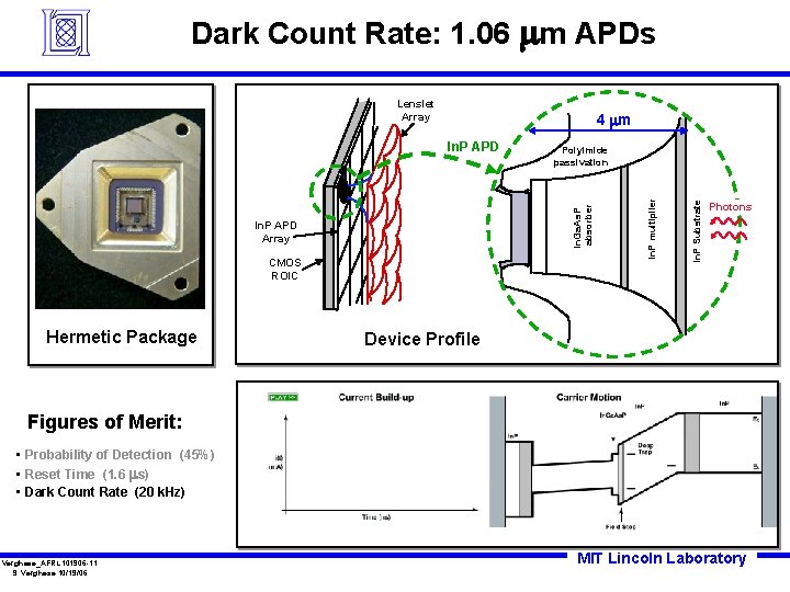
Dark Count Rate: 1. 06 mm APDs Lenslet Array 4 mm In. P Substrate CMOS ROIC In. P multiplier In. P APD Array Hermetic Package Polyimide passivation In. Ga. As. P absorber In. P APD Photons Device Profile Figures of Merit: • Probability of Detection (45%) • Reset Time (1. 6 ms) • Dark Count Rate (20 k. Hz) Verghese_AFRL 101906 -11 S. Verghese 10/19/06 MIT Lincoln Laboratory
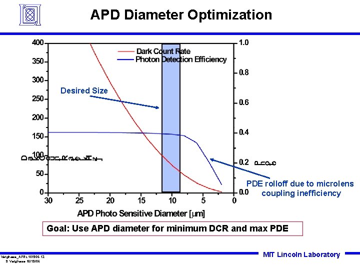
APD Diameter Optimization Desired Size PDE rolloff due to microlens coupling inefficiency Goal: Use APD diameter for minimum DCR and max PDE Verghese_AFRL 101906 -12 S. Verghese 10/19/06 MIT Lincoln Laboratory
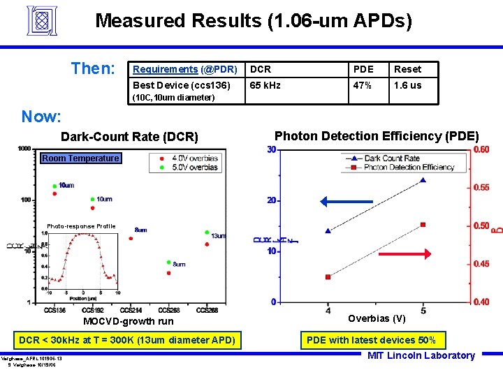
Measured Results (1. 06 -um APDs) Then: Requirements (@PDR) DCR PDE Reset Best Device (ccs 136) 65 k. Hz 47% 1. 6 us (10 C, 10 um diameter) Now: Dark-Count Rate (DCR) Photon Detection Efficiency (PDE) Room Temperature Photo-response Profile Effective device diameter MOCVD-growth run DCR < 30 k. Hz at T = 300 K (13 um diameter APD) Verghese_AFRL 101906 -13 S. Verghese 10/19/06 Overbias (V) PDE with latest devices 50% MIT Lincoln Laboratory
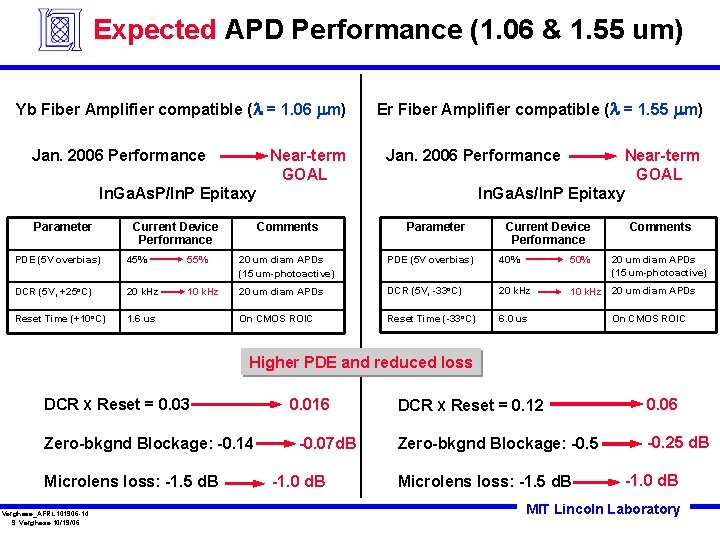
Expected APD Performance (1. 06 & 1. 55 um) Yb Fiber Amplifier compatible (l = 1. 06 mm) Jan. 2006 Performance Near-term GOAL Er Fiber Amplifier compatible (l = 1. 55 mm) Jan. 2006 Performance Near-term GOAL In. Ga. As/In. P Epitaxy In. Ga. As. P/In. P Epitaxy Parameter Current Device Performance Comments PDE (5 V overbias) 45% 55% 20 um diam APDs (15 um-photoactive) PDE (5 V overbias) 40% 50% 20 um diam APDs (15 um-photoactive) DCR (5 V, +25 o. C) 20 k. Hz 10 k. Hz 20 um diam APDs DCR (5 V, -33 o. C) 20 k. Hz 10 k. Hz 20 um diam APDs Reset Time (+10 o. C) 1. 6 us On CMOS ROIC Reset Time (-33 o. C) 6. 0 us On CMOS ROIC Higher PDE and reduced loss DCR X Reset = 0. 03 Zero-bkgnd Blockage: -0. 14 Microlens loss: -1. 5 d. B Verghese_AFRL 101906 -14 S. Verghese 10/19/06 0. 016 -0. 07 d. B -1. 0 d. B DCR X Reset = 0. 12 0. 06 Zero-bkgnd Blockage: -0. 5 -0. 25 d. B Microlens loss: -1. 5 d. B -1. 0 d. B MIT Lincoln Laboratory
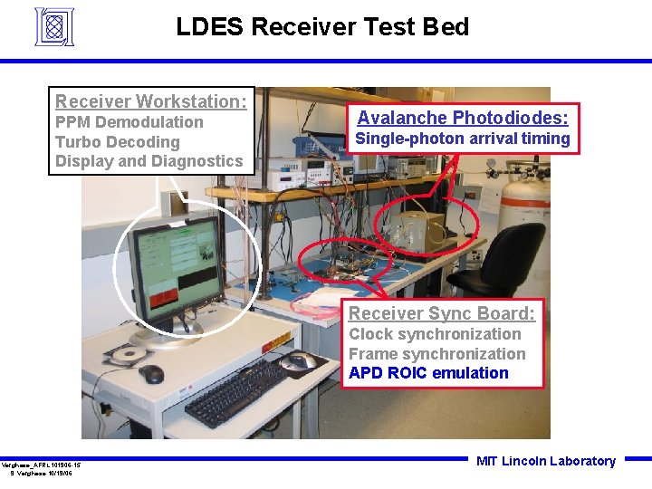
LDES Receiver Test Bed Receiver Workstation: PPM Demodulation Turbo Decoding Display and Diagnostics Avalanche Photodiodes: Single-photon arrival timing Receiver Sync Board: Clock synchronization Frame synchronization APD ROIC emulation Verghese_AFRL 101906 -15 S. Verghese 10/19/06 MIT Lincoln Laboratory
Current development in LADAR APDs Metric • Increased Array Size Requirement • Uniformity 256 x 64, 50 mm • • Reduced Pixel Size 3 D Integration In. P 5 V SOI 2 V SOI Verghese_AFRL 101906 -16 S. Verghese 10/19/06 Carrier wafer • Enhanced Processing, Functionality • Fast Reset, Counting, Low Jitter, Caching • Spectral Coverage • Other Materials MIT Lincoln Laboratory
In. P Avalanche Photodiodes • • • Introduction Applications APD Figures of Merit – Photon Detection Efficiency (PDE) – Reset Time – Dark Count Rate (DCR) • • Verghese_AFRL 101906 -17 S. Verghese 10/19/06 Read-Out Integrated Circuit (ROIC) Summary MIT Lincoln Laboratory
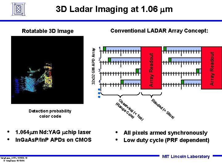
3 D Ladar Imaging at 1. 06 mm Conventional LADAR Array Concept: Detection probability color code • • 1. 064 mm Nd: YAG mchip laser In. Ga. As. P/In. P APDs on CMOS Verghese_AFRL 101906 -18 S. Verghese 10/19/06 Array Readout 1 Array Readout 32 x 32 GM-APD Array Rotatable 3 D Image 2 3 4 Bl O (R bse an rv ge ing Ga (< te 1 u ) s in de d ) • • (> 50 us ) All pixels armed synchronously Low duty cycle (PRF dependent) MIT Lincoln Laboratory
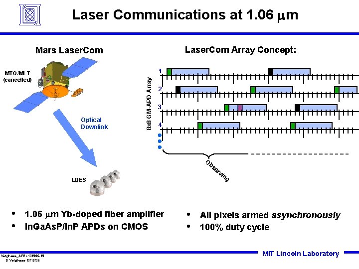
Laser Communications at 1. 06 mm Laser. Com Array Concept: Mars Laser. Com Optical Downlink 8 x 8 GM-APD Array 1 MTO/MLT (cancelled) 2 3 4 Ob se r vi n g LDES • • 1. 06 mm Yb-doped fiber amplifier In. Ga. As. P/In. P APDs on CMOS Verghese_AFRL 101906 -19 S. Verghese 10/19/06 • • All pixels armed asynchronously 100% duty cycle MIT Lincoln Laboratory
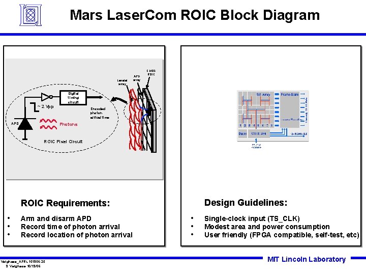
Mars Laser. Com ROIC Block Diagram Lenslet array ~ 2 Vpp APD array CMOS ROIC Digital timing circuit Encoded photon arrival time Photons ROIC Pixel Circuit Design Guidelines: ROIC Requirements: • • • Arm and disarm APD Record time of photon arrival Record location of photon arrival Verghese_AFRL 101906 -20 S. Verghese 10/19/06 • • • Single-clock input (TS_CLK) Modest area and power consumption User friendly (FPGA compatible, self-test, etc) MIT Lincoln Laboratory
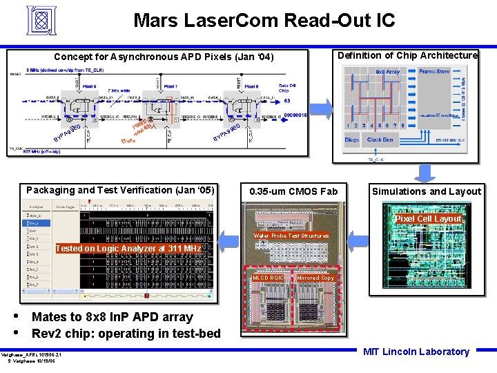
Mars Laser. Com Read-Out IC Definition of Chip Architecture Concept for Asynchronous APD Pixels (Jan ‘ 04) D SE AS YP B ED SS A YP B Packaging and Test Verification (Jan ‘ 05) 0. 35 -um CMOS Fab Simulations and Layout Pixel Cell Layout Wafer-Probe Test Structures Tested on Logic Analyzer at 311 MHz MLCD ROIC • • Mirrored Copy Mates to 8 x 8 In. P APD array Rev 2 chip: operating in test-bed Verghese_AFRL 101906 -21 S. Verghese 10/19/06 MIT Lincoln Laboratory
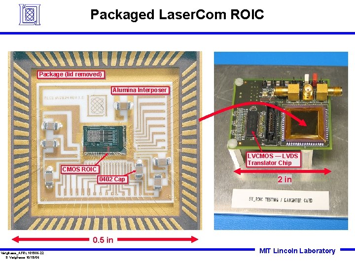
Packaged Laser. Com ROIC Package (lid removed) Alumina Interposer LVCMOS — LVDS Translator Chip CMOS ROIC 0402 Cap 2 in 0. 5 in Verghese_AFRL 101906 -22 S. Verghese 10/19/06 MIT Lincoln Laboratory
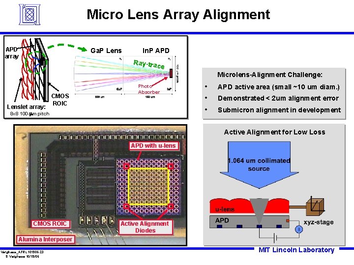
Micro Lens Array Alignment APD array Ga. P Lens In. P APD Ray-trac e Microlens-Alignment Challenge: Lenslet array: CMOS ROIC Photo Absorber 8 x 8 100 -mm pitch • • • APD active area (small ~10 um diam. ) Demonstrated < 2 um alignment error Submicron alignment in development Active Alignment for Low Loss APD with u-lens CMOS ROIC Active Alignment Diodes Alumina Interposer Verghese_AFRL 101906 -23 S. Verghese 10/19/06 MIT Lincoln Laboratory
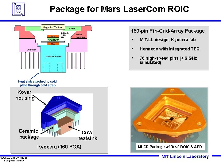
Package for Mars Laser. Com ROIC 160 -pin Pin-Grid-Array Package • MIT/LL design; Kyocera fab • Hermetic with integrated TEC • 70 high-speed pins (< 6 GHz simulated) Kovar housing Ceramic package Cu. W heatsink Kyocera (160 PGA) Verghese_AFRL 101906 -24 S. Verghese 10/19/06 MLCD Package w/ Rev 2 ROIC & APD MIT Lincoln Laboratory
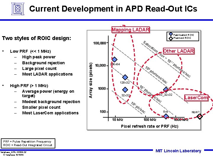
Current Development in APD Read-Out ICs Mapping LADAR Two styles of ROIC design: • Low PRF (<< 1 MHz) – High peak power – Background rejection – Large pixel count – Most LADAR applications High PRF (> 1 MHz) – Average power (energy on target) – Modest background rejection – Smaller pixel count – Most Laser. Com applications Sa tu 100, 000 Array size (pixels) • 10, 000 Fabricated ROIC Planned ROIC ra 256 x 64 10 9 tio n 10 7 1000 ph 32 x 32 10 5 ph on 10 k. Hz = 10 1 1 ph s/ on USD_32 x 32 s/ se c /s e on s/ se c ot c 100 ux ot ph ot 128 x 32 Other LADAR Fl Laser. Com 8 x 8 100 k. Hz Nb. N? 1000 k. Hz Pixel refresh rate or PRF (Hz) PRF = Pulse Repetition Frequency ROIC = Read-Out Integrated Circuit Verghese_AFRL 101906 -25 S. Verghese 10/19/06 MIT Lincoln Laboratory
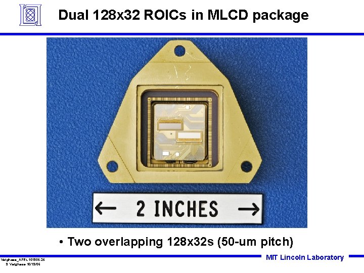
Dual 128 x 32 ROICs in MLCD package • Two overlapping 128 x 32 s (50 -um pitch) Verghese_AFRL 101906 -26 S. Verghese 10/19/06 MIT Lincoln Laboratory
In. P APDs: Summary • We built and demonstrated integrated In. P APD arrays for Laser. Com and LADAR – In. Ga. As. P/In. P for 1. 06 -um wavelength – In. Ga. As for 1. 55 -um wavelength (less mature) • Current focus: – Increasing Photon Detection Efficiency – Decreasing Dark Count Rate • Hybrid-assembly of In. P arrays with Si CMOS enables: – High fill-factor photon counters (up to 4 kpixels) – Compact, low-power sensor (plugs into a pc board) Verghese_AFRL 101906 -27 S. Verghese 10/19/06 MIT Lincoln Laboratory
End S. Verghese MIT Lincoln Laboratory Verghese_AFRL 101906 -28 S. Verghese 10/19/06
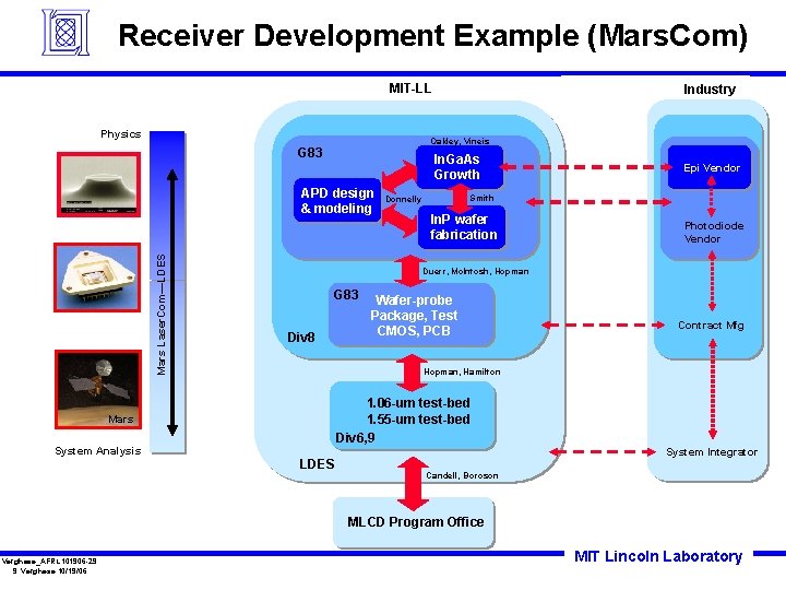
Receiver Development Example (Mars. Com) MIT-LL Physics Oakley, Vineis G 83 In. Ga. As Growth APD design & modeling Mars Laser. Com—LDES Industry Epi Vendor Smith Donnelly In. P wafer fabrication Photodiode Vendor Duerr, Mc. Intosh, Hopman G 83 Div 8 Wafer-probe Package, Test CMOS, PCB Contract Mfg Hopman, Hamilton 1. 06 -um test-bed 1. 55 -um test-bed Div 6, 9 Mars System Analysis LDES System Integrator Candell, Boroson MLCD Program Office Verghese_AFRL 101906 -29 S. Verghese 10/19/06 MIT Lincoln Laboratory