Characterization of Silicon Photodetectors Avalanche Photodiodes in Geiger
- Slides: 34

Characterization of Silicon Photodetectors (Avalanche Photodiodes in Geiger Mode) at Fermilab G. Mavromanolakis, A. Para. N. Saoulidou Novel Phot. Detectors 07, Kobe, June 27, 2007

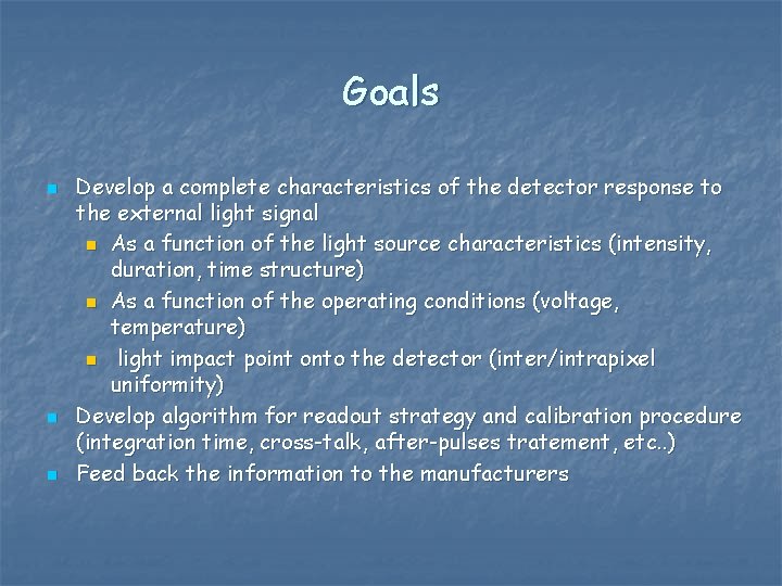
Goals n n n Develop a complete characteristics of the detector response to the external light signal n As a function of the light source characteristics (intensity, duration, time structure) n As a function of the operating conditions (voltage, temperature) n light impact point onto the detector (inter/ intrapixel uniformity) Develop algorithm for readout strategy and calibration procedure (integration time, cross-talk, after-pulses tratement, etc. . ) Feed back the information to the manufacturers

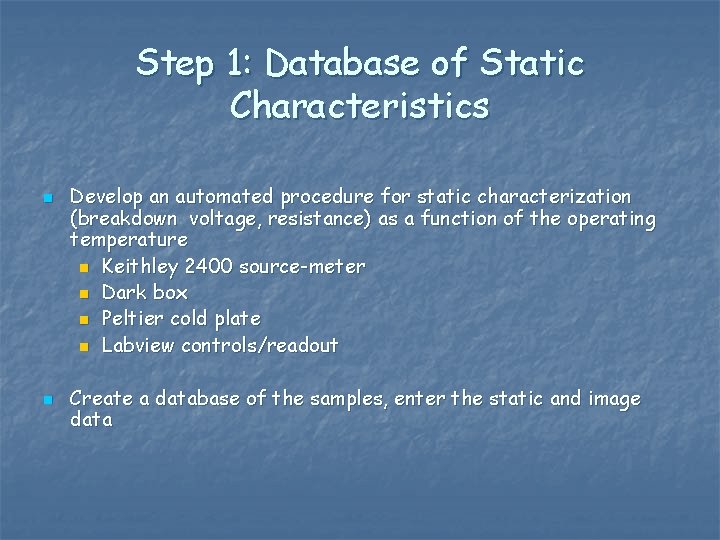
Step 1: Database of Static Characteristics n n Develop an automated procedure for static characterization (breakdown voltage, resistance) as a function of the operating temperature n Keithley 2400 source-meter n Dark box n Peltier cold plate n Labview controls/readout Create a database of the samples, enter the static and image data

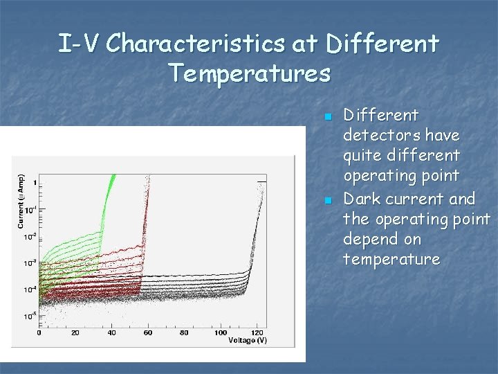
I-V Characteristics at Different Temperatures n n Different detectors have quite different operating point Dark current and the operating point depend on temperature

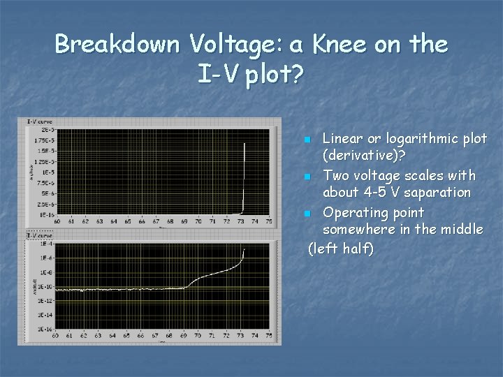
Breakdown Voltage: a Knee on the I-V plot? Linear or logarithmic plot (derivative)? n Two voltage scales with about 4 -5 V saparation n Operating point somewhere in the middle (left half) n

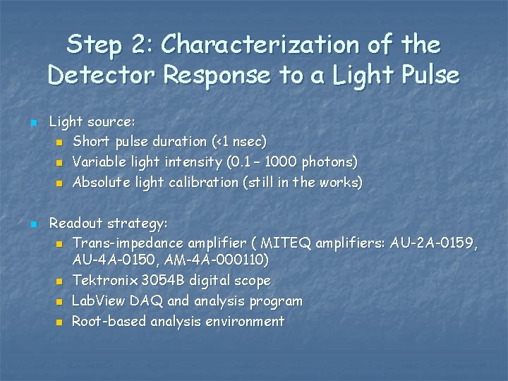
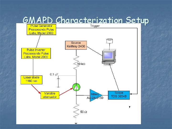
Step 2: Characterization of the Detector Response to a Light Pulse n n Light source: n Short pulse duration (<1 nsec) n Variable light intensity (0. 1 – 1000 photons) n Absolute light calibration (still in the works) Readout strategy: n Trans-impedance amplifier ( MITEQ amplifiers: AU-2 A-0159, AU-4 A-0150, AM-4 A-000110) n Tektronix 3054 B digital scope n Lab. View DAQ and analysis program n Root-based analysis environment

GMAPD Characterization Setup

Disclaimer n n n The following ‘results’ are primarily meant to demonstrate the scope of the data collected. Two analysis chain (root-based and Labview-based) have been just established The results and tentative conclusions are preliminary and are meant as ‘food for thought’ Results shown will be for Hamamatsu MPPC 025 U detector There are much more results coming, the analysis just started last week.

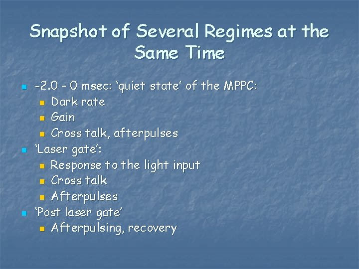
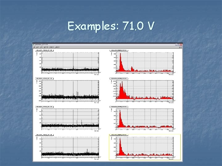
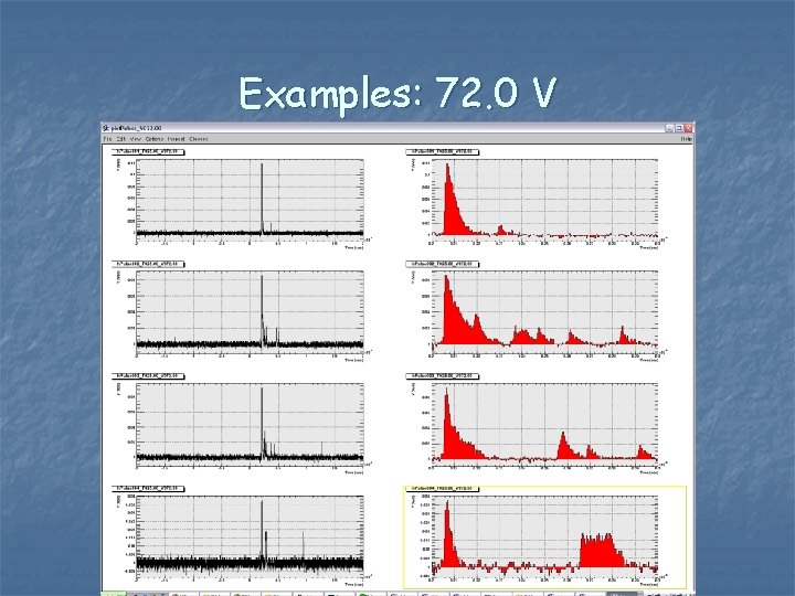
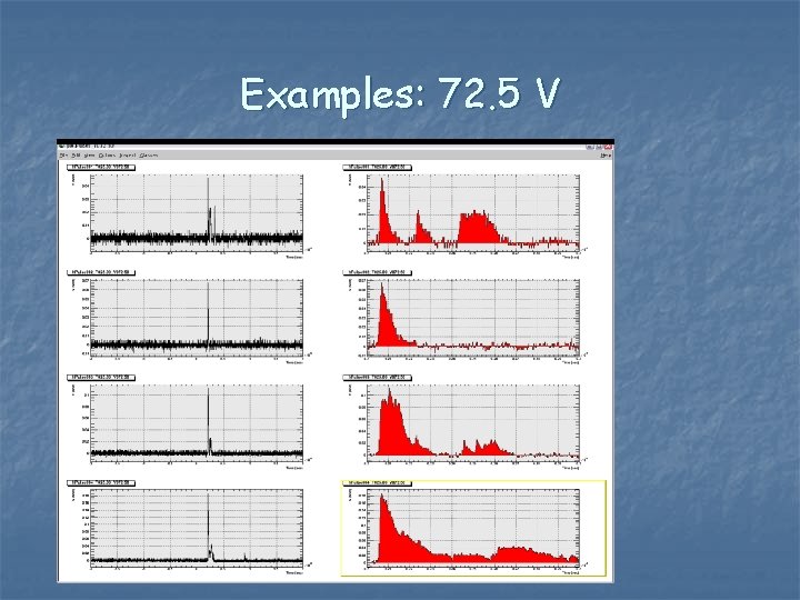
Snapshot of Several Regimes at the Same Time n n n -2. 0 – 0 msec: ‘quiet state’ of the MPPC: n Dark rate n Gain n Cross talk, afterpulses ‘Laser gate’: n Response to the light input n Cross talk n Afterpulses ‘Post laser gate’ n Afterpulsing, recovery

Examples: 71. 0 V

Examples: 72. 0 V

Examples: 72. 5 V

Salient Features: Detector Instabilities n n Often called cross-talk, afterpulsing, etc. These instabilities determine the nature of the response of the detector in a manner which depends on the temporal characteristic of the measured light and/or on the characteristics of the read-out electronics It is very important to understand their origin and to reduce their incidence Tens of years of R&D for the SPAD detectors should be of great help

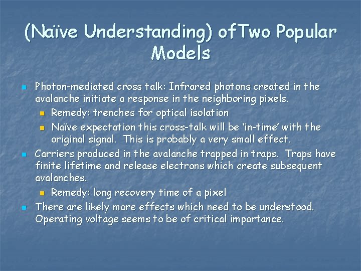
(Naïve Understanding) of. Two Popular Models n n n Photon-mediated cross talk: Infrared photons created in the avalanche initiate a response in the neighboring pixels. n Remedy: trenches for optical isolation n Naïve expectation this cross-talk will be ‘in-time’ with the original signal. This is probably a very small effect. Carriers produced in the avalanche trapped in traps. Traps have finite lifetime and release electrons which create subsequent avalanches. n Remedy: long recovery time of a pixel There are likely more effects which need to be understood. Operating voltage seems to be of critical importance.

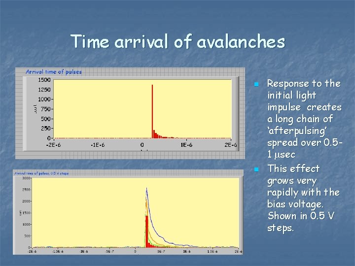
Time arrival of avalanches n n Response to the initial light impulse creates a long chain of ‘afterpulsing’ spread over 0. 51 msec This effect grows very rapidly with the bias voltage. Shown in 0. 5 V steps.

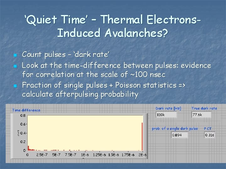
‘Quiet Time’ – Thermal Electrons. Induced Avalanches? n n n Count pulses – ‘dark rate’ Look at the time-difference between pulses: evidence for correlation at the scale of ~100 nsec Fraction of single pulses + Poisson statistics => calculate afterpulsing probability

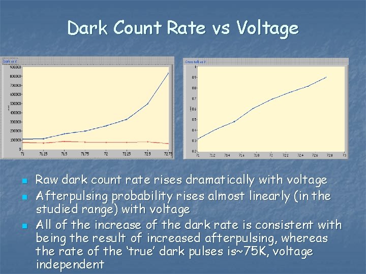
Dark Count Rate vs Voltage n n n Raw dark count rate rises dramatically with voltage Afterpulsing probability rises almost linearly (in the studied range) with voltage All of the increase of the dark rate is consistent with being the result of increased afterpulsing, whereas the rate of the ‘true’ dark pulses is~75 K, voltage independent

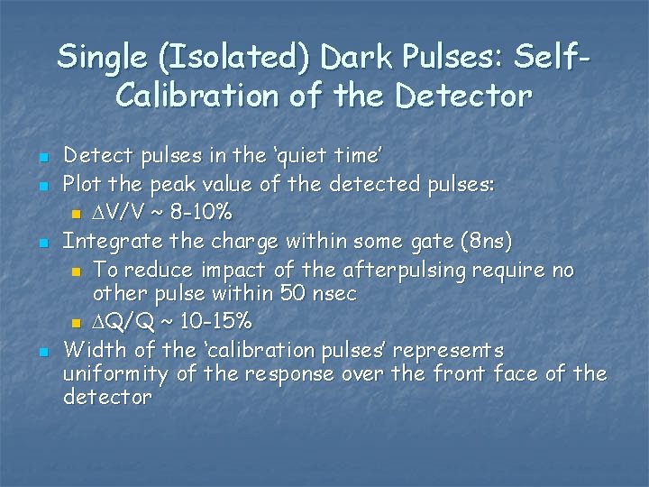
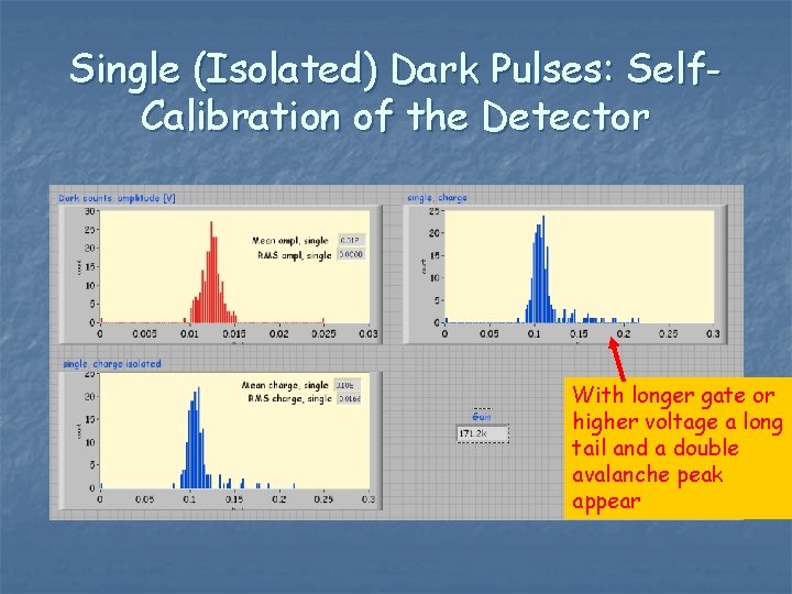
Single (Isolated) Dark Pulses: Self. Calibration of the Detector n n Detect pulses in the ‘quiet time’ Plot the peak value of the detected pulses: n DV/V ~ 8 -10% Integrate the charge within some gate (8 ns) n To reduce impact of the afterpulsing require no other pulse within 50 nsec n DQ/Q ~ 10 -15% Width of the ‘calibration pulses’ represents uniformity of the response over the front face of the detector

Single (Isolated) Dark Pulses: Self. Calibration of the Detector With longer gate or higher voltage a long tail and a double avalanche peak appear

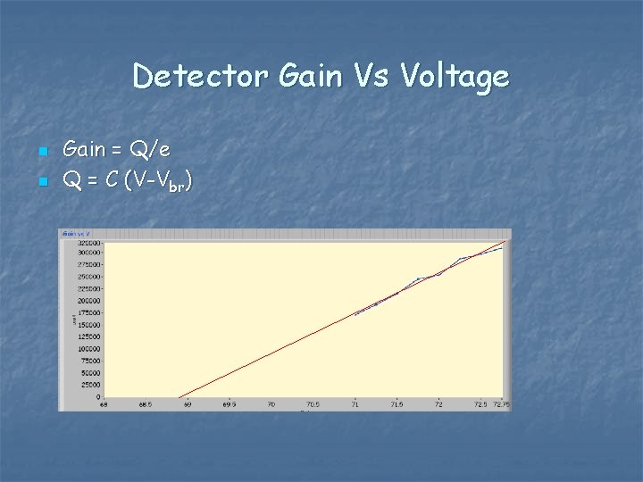
Detector Gain Vs Voltage n n Gain = Q/e Q = C (V-Vbr)

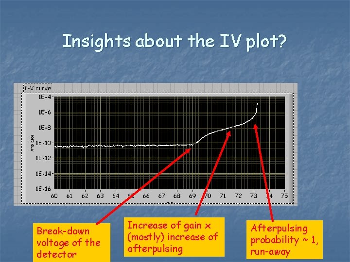
Insights about the IV plot? Break-down voltage of the detector Increase of gain x (mostly) increase of afterpulsing Afterpulsing probability ~ 1, run-away

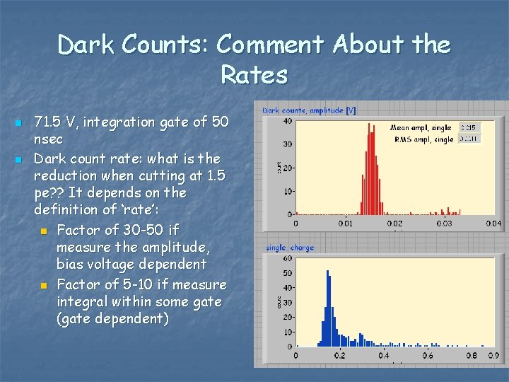
Dark Counts: Comment About the Rates n n 71. 5 V, integration gate of 50 nsec Dark count rate: what is the reduction when cutting at 1. 5 pe? ? It depends on the definition of ‘rate’: n Factor of 30 -50 if measure the amplitude, bias voltage dependent n Factor of 5 -10 if measure integral within some gate (gate dependent)

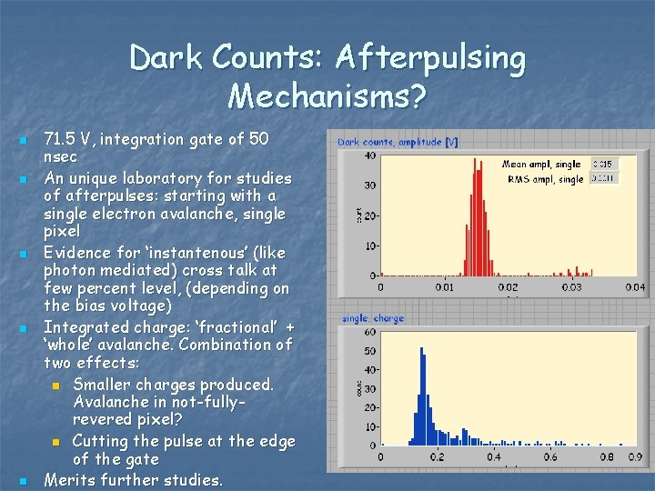
Dark Counts: Afterpulsing Mechanisms? n n n 71. 5 V, integration gate of 50 nsec An unique laboratory for studies of afterpulses: starting with a single electron avalanche, single pixel Evidence for ‘instantenous’ (like photon mediated) cross talk at few percent level, (depending on the bias voltage) Integrated charge: ‘fractional’ + ‘whole’ avalanche. Combination of two effects: n Smaller charges produced. Avalanche in not-fullyrevered pixel? n Cutting the pulse at the edge of the gate Merits further studies.

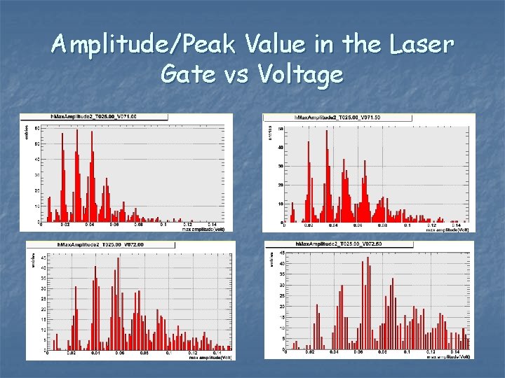
Amplitude/Peak Value in the Laser Gate vs Voltage

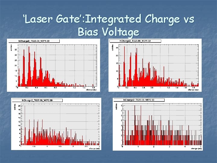
‘Laser Gate’: Integrated Charge vs Bias Voltage

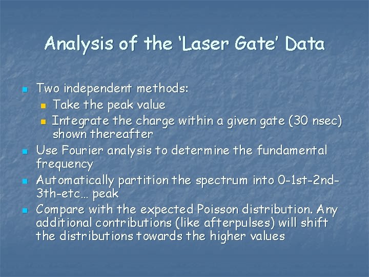
Analysis of the ‘Laser Gate’ Data n n Two independent methods: n Take the peak value n Integrate the charge within a given gate (30 nsec) shown thereafter Use Fourier analysis to determine the fundamental frequency Automatically partition the spectrum into 0 -1 st-2 nd 3 th-etc… peak Compare with the expected Poisson distribution. Any additional contributions (like afterpulses) will shift the distributions towards the higher values

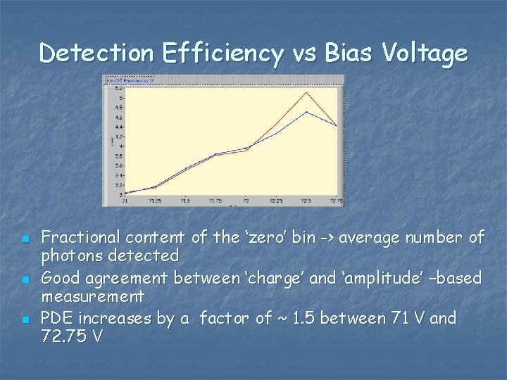
Detection Efficiency vs Bias Voltage n n n Fractional content of the ‘zero’ bin -> average number of photons detected Good agreement between ‘charge’ and ‘amplitude’ –based measurement PDE increases by a factor of ~ 1. 5 between 71 V and 72. 75 V

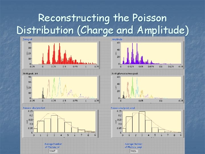
Reconstructing the Poisson Distribution (Charge and Amplitude)

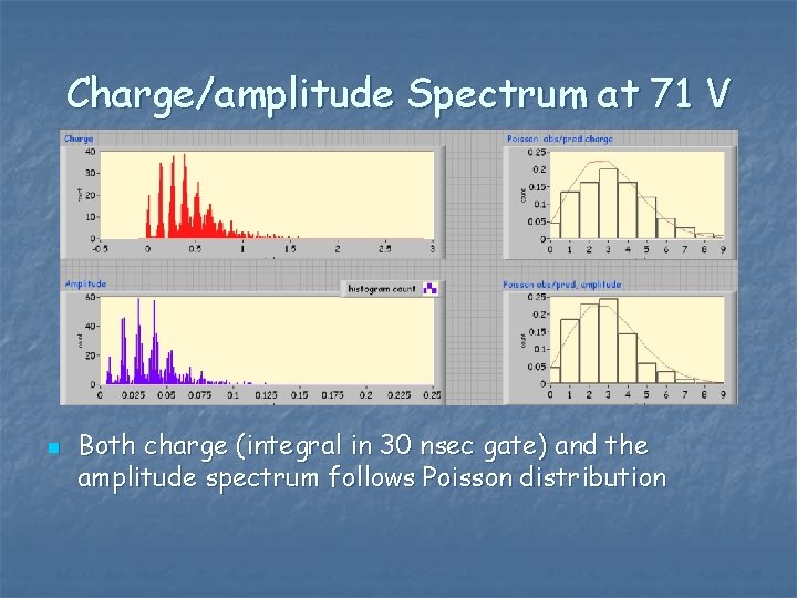
Charge/amplitude Spectrum at 71 V n Both charge (integral in 30 nsec gate) and the amplitude spectrum follows Poisson distribution

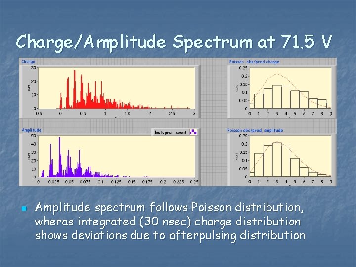
Charge/Amplitude Spectrum at 71. 5 V n Amplitude spectrum follows Poisson distribution, wheras integrated (30 nsec) charge distribution shows deviations due to afterpulsing distribution

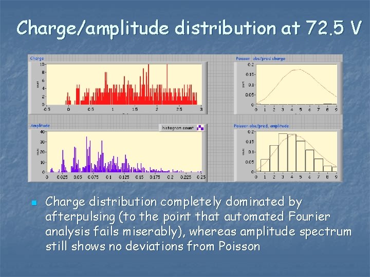
Charge/amplitude distribution at 72. 5 V n Charge distribution completely dominated by afterpulsing (to the point that automated Fourier analysis fails miserably), whereas amplitude spectrum still shows no deviations from Poisson

Lessons From the Charge/Amplitude Comparison n n Amplitude spectrum is not sensitive to afterpulsing but it is sensitive to the instantaneous cross-talk (like photon-mediated). Amplitude spectrum shows no deviation from Poisson, hence the ‘instantaneous’ cross-talk is a very small effe Charge distribution is very sensitive to the integration gate. Even with 30 nsec gate it shows huge effects (and deviations from Poisson distribution). This effect is a very strong function of the bias voltage. The time scale (30 nsec) seems to indicate that these afterpulses are generated in different pixels (no trapping model) What is the mechanism of cross talk at the timescales of the order of tens of nsecs? ? ?

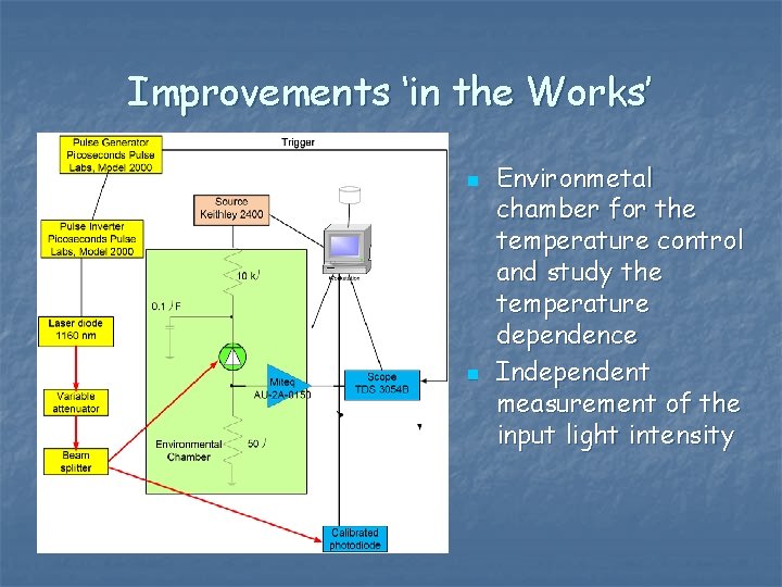
Improvements ‘in the Works’ n n Environmetal chamber for the temperature control and study the temperature dependence Independent measurement of the input light intensity

Conclusions n n Waveforms produced by GMAPD’s under different conditions provide wealth of information about properties and behavior of the detectors Detector instabilities (cross-talk, afterpulsing) are major contribution to the detector response. Their practical consequences depend on the readout details and the experimental conditions (temporal structure of the measured light pulses) Physics of afterpulsing is likely to be rather complicated A lot more understanding can be achieved from the existing setups/data, but (perhaps) special detector samples (different recovery time, different number of pixels of a given size) could be very helpful in disentangling various contributions.
 Photodiode current equation
 Qlids
Qlids Avalanche terminology
 معنیroots
 Avalanche rpc
 Class 5 avalanche
 What are avalanche transit time devices
 Avalanche effect in des with example
 Alptruth avalanche
 Avalanche
 The avalanche devoured everything in its path
 Geiger mullerův počítač
 Cholesteramin
 Quantum random number generator usb
 Jeanne geiger crisis center
 Geiger counter youtube
 Michael geiger uml
 Hans geiger atomic theory
 Compteur geiger-müller
 Geiger counter
 Fission equation
 Michael geiger uml
 Região concentrada
 In the fog by milton geiger story
 Nuclide representation
 Geiger
 Reaciton
 What does indirect characterization mean
 Definition for direct characterization
 Etch silicon
 Silicon valley xray
 Septa prefix
 An industrially important element contains 26
 Chemical formula covalent compounds
 Cz silicon wafer with high resistivity
