Manufacture of High Resistivity Low Oxygen Czochralski Silicon
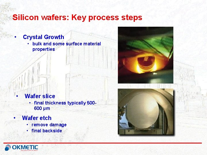
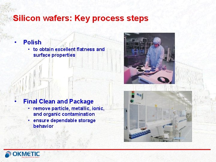
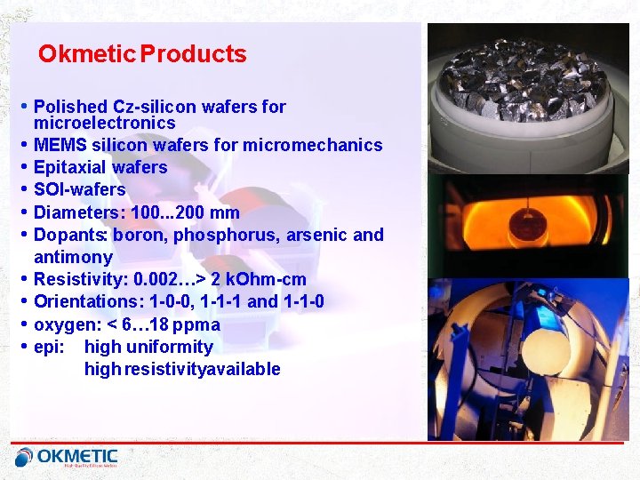
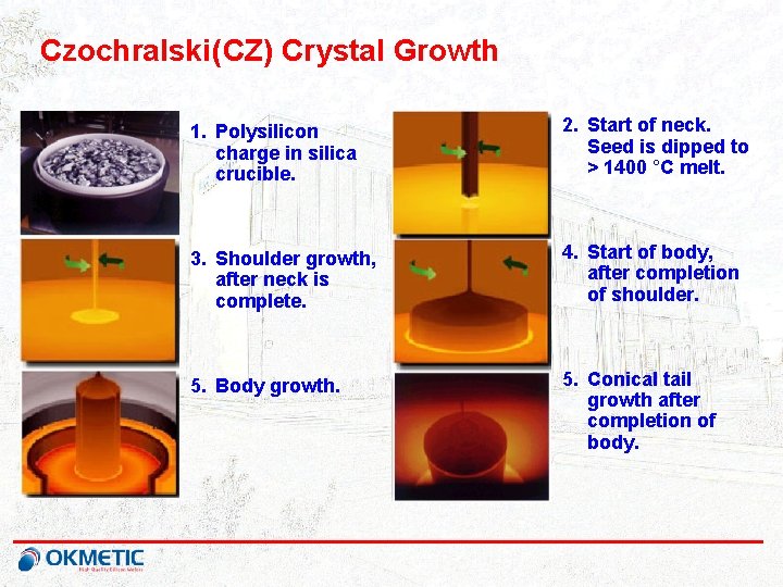

- Slides: 39

Manufacture of High Resistivity, Low Oxygen Czochralski Silicon June 2005 Olli Anttila Okmetic Fellow, Okmetic Oyj

Manufacture of High Resistivity, Low Oxygen Czochralski Silicon Outline • • Background Crystal growth and wafer manufacturing Wafer characteristics High resistivity. CZ • Metals and lifetime • Dopants • Oxygen • Magnetic field • Silicon melt behavior • Conclusions

Okmetic Worldwide Presence

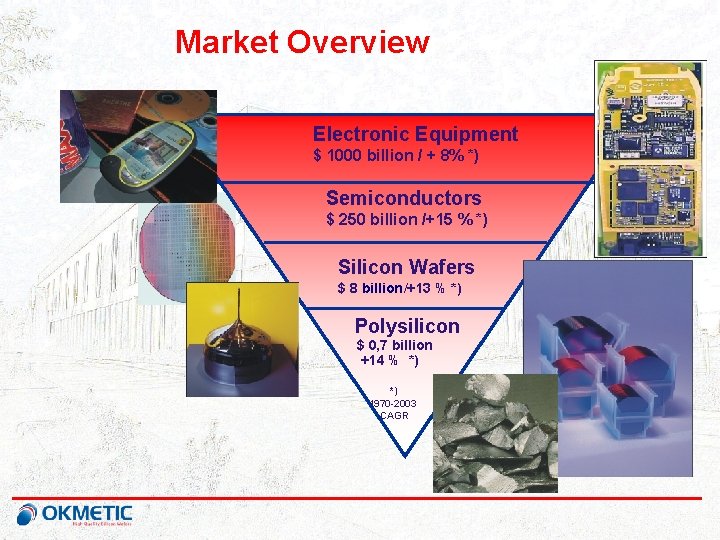
Market Overview Electronic Equipment $ 1000 billion / + 8% *) ©NOKIA MEGATRENDS. PPT / 16. 11. 1998 EKu / page: 6 Semiconductors $ 250 billion /+15 % *) Silicon Wafers $ 8 billion /+13 % *) Polysilicon $ 0, 7 billion +14 % *) *) 1970 -2003 CAGR

Silicon wafers: Key process steps • Crystal Growth • bulk and some surface material properties • Wafer slice • final thickness typically 500600 µm • Wafer etch • remove damage • final backside

Silicon wafers: Key process steps • Polish • to obtain excellent flatness and surface properties • Final Clean and Package • remove particle, metallic, ionic, and organic contamination • ensure dependable storage behavior

Okmetic Products • Polished Cz-silicon wafers for • • • microelectronics MEMS silicon wafers for micromechanics Epitaxial wafers SOI-wafers Diameters: 100. . . 200 mm Dopants: boron, phosphorus, arsenic and antimony Resistivity: 0. 002…> 2 k. Ohm-cm Orientations: 1 -0 -0, 1 -1 -1 and 1 -1 -0 oxygen: < 6… 18 ppma epi: high uniformity high resistivityavailable

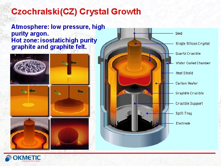
Czochralski (CZ) Crystal Growth 1. Polysilicon charge in silica crucible. 2. Start of neck. Seed is dipped to > 1400 °C melt. 3. Shoulder growth, after neck is complete. 4. Start of body, after completion of shoulder. 5. Body growth. 5. Conical tail growth after completion of body.

Czochralski (CZ) Crystal Growth Atmosphere: low pressure, high purity argon. Hot zone: isostatichigh purity graphite and graphite felt.

Manufacture of High Resistivity, Low Oxygen Czochralski Silicon Outline • • Background Crystal growth and wafer manufacturing Wafer characteristics: lifetime and metals High resistivity. CZ • Metals and lifetime • Dopants • Oxygen • Magnetic field • Silicon melt behavior • Conclusions

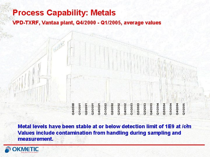
Process Capability: Metals VPD-TXRF, Vantaa plant, Q 4/2000 - Q 1/2005, average values 2. Metal levels have been stable at or below detection limit of 1 E 9 at /cm Values include contamination from handling during sampling and measurement.

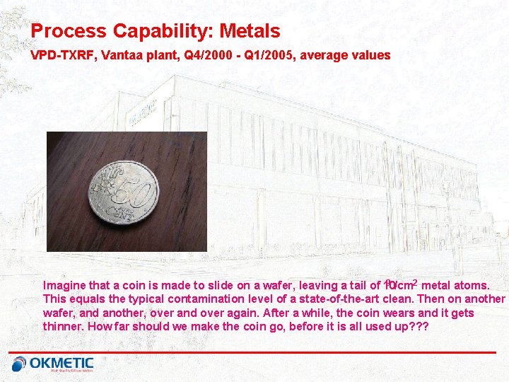
Process Capability: Metals VPD-TXRF, Vantaa plant, Q 4/2000 - Q 1/2005, average values 9 /cm 2 metal atoms. Imagine that a coin is made to slide on a wafer, leaving a tail of 10 This equals the typical contamination level of a state-of-the-art clean. Then on another wafer, and another, over and over again. After a while, the coin wears and it gets thinner. How far should we make the coin go, before it is all used up? ? ?

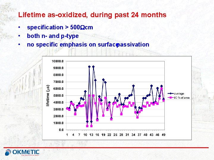
Lifetime as-oxidized, during past 24 months • • • specification > 500 Wcm both n- and p-type no specific emphasis on surfacepassivation

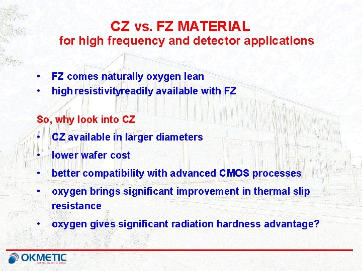
CZ vs. FZ MATERIAL for high frequency and detector applications • • FZ comes naturally oxygen lean high resistivityreadily available with FZ So, why look into CZ • CZ available in larger diameters • lower wafer cost • better compatibility with advanced CMOS processes • oxygen brings significant improvement in thermal slip resistance • oxygen gives significant radiation hardness advantage?

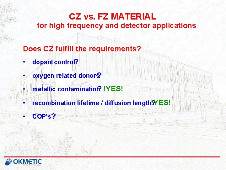
CZ vs. FZ MATERIAL for high frequency and detector applications Does CZ fulfill the requirements? • dopant control? • oxygen related donors? • metallic contamination ? !YES! • recombination lifetime / diffusion length? !YES! • COP’s?

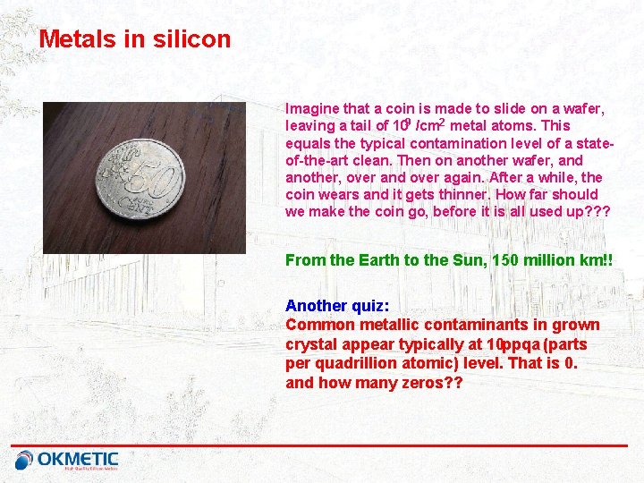
Metals in silicon Imagine that a coin is made to slide on a wafer, leaving a tail of 109 /cm 2 metal atoms. This equals the typical contamination level of a stateof-the-art clean. Then on another wafer, and another, over and over again. After a while, the coin wears and it gets thinner. How far should we make the coin go, before it is all used up? ? ? From the Earth to the Sun, 150 million km!! Another quiz: Common metallic contaminants in grown crystal appear typically at 10 ppqa (parts per quadrillion atomic) level. That is 0. and how many zeros? ?

CZ vs. FZ MATERIAL for high frequency and detector applications Does CZ fulfill the requirements? • dopant control? • oxygen related donors? • metallic contamination ? !YES! • recombination lifetime / diffusion length? !YES! • COP’s?

HIGH RESISTIVITY MATERIAL: 6”P 100 normal crucible quality • Intentional doping at about 1600 Ohmcm level at seed end. • Typical seed-to-tailresistivityratio is about 1. 5; here much larger. • High crucible boron (& Al) content results in < k. Ohmcm 1 material.

HIGH RESISTIVITY MATERIAL: 6”P 100 synthetic crucible • • • special Si. O 2 coating resistivityat seed end is higher due to oxygen donors boron contamination in some critical graphite parts

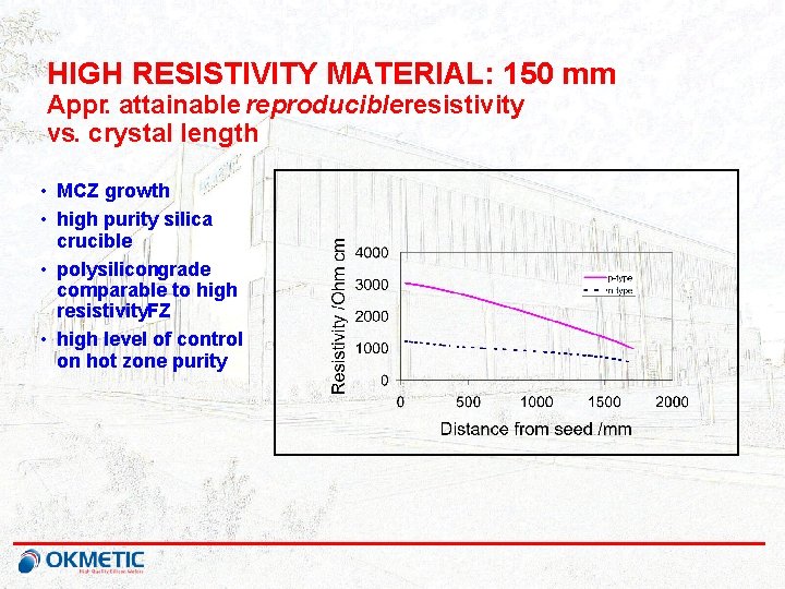
HIGH RESISTIVITY MATERIAL: 150 mm Appr. attainable reproducibleresistivity vs. crystal length • MCZ growth • high purity silica crucible • polysilicongrade comparable to high resistivity. FZ • high level of control on hot zone purity

CZ vs. FZ MATERIAL for high frequency and detector applications Does CZ fulfill the requirements? • dopant control? !YES? • oxygen related donors? • metallic contamination ? !YES! • recombination lifetime / diffusion length? !YES! • COP’s?

HIGH RESISTIVITY CZ MATERIAL • low interstitial oxygen mandatory • oxygen donors created during crystal growth and device process • critical temperatureappr. 450 °C • donors annihilated > 600 °C • back-end-of-the-line (BEOL) temperatures between 400 and 500 °C to be avoided • e. g. , at 420 °C, only 10 -30 min allowed, depending on Oi and resistivity • typical Oi 5 -8 ppma for high res. material

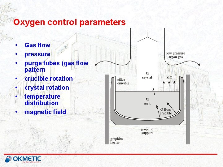
Oxygen control parameters • • Gas flow pressure purge tubes (gas flow pattern crucible rotation crystal rotation temperature distribution magnetic field

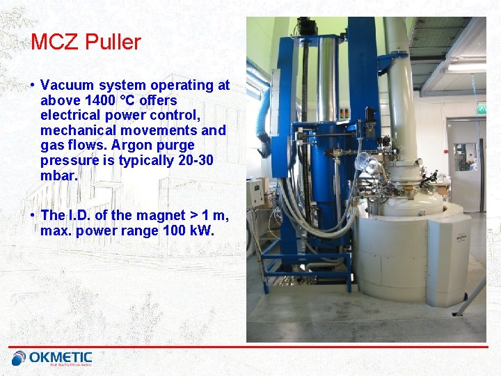
MCZ Puller • Vacuum system operating at above 1400 °C offers electrical power control, mechanical movements and gas flows. Argon purge pressure is typically 20 -30 mbar. • The I. D. of the magnet > 1 m, max. power range 100 k. W.

MCZ stabilizes the melt and has some influence on oxygen level Results from early crystals ~10 yrs. ago • magnet used by. Okmetic results to somewhathigher oxygen level than regular CZ • better melt stabilitywidens oxygen range; more aggressive control parameters can be used

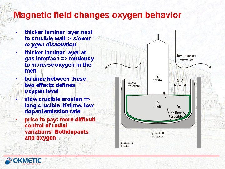
Magnetic field changes oxygen behavior • • • thicker laminar layer next to crucible wall=> slower oxygen dissolution thicker laminar layer at gas interface => tendency to increase oxygen in the melt balance between these two effects defines oxygen level slow crucible erosion => long crucible lifetime, low dopant emission rate price to pay: more difficult control of radial variations! Bothdopants and oxygen

CZ vs. FZ MATERIAL for high frequency and detector applications Does CZ fulfill the requirements? • dopant control? !YES? • oxygen related donors? !YES? • metallic contamination ? !YES! • recombination lifetime / diffusion length? !YES! • COP’s? remains unresolved at this point, and should be addressed later, if needed; typical density < 1 E 6 /cc.

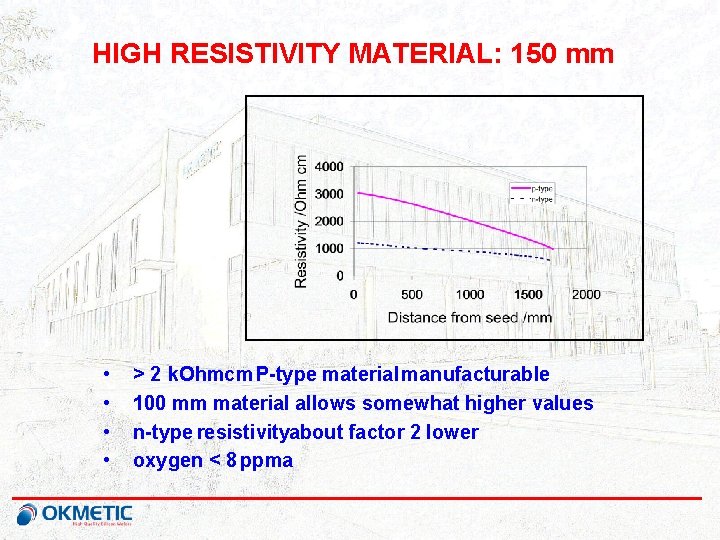
HIGH RESISTIVITY MATERIAL: 150 mm • • > 2 k. Ohmcm P-type material manufacturable 100 mm material allows somewhat higher values n-type resistivityabout factor 2 lower oxygen < 8 ppma

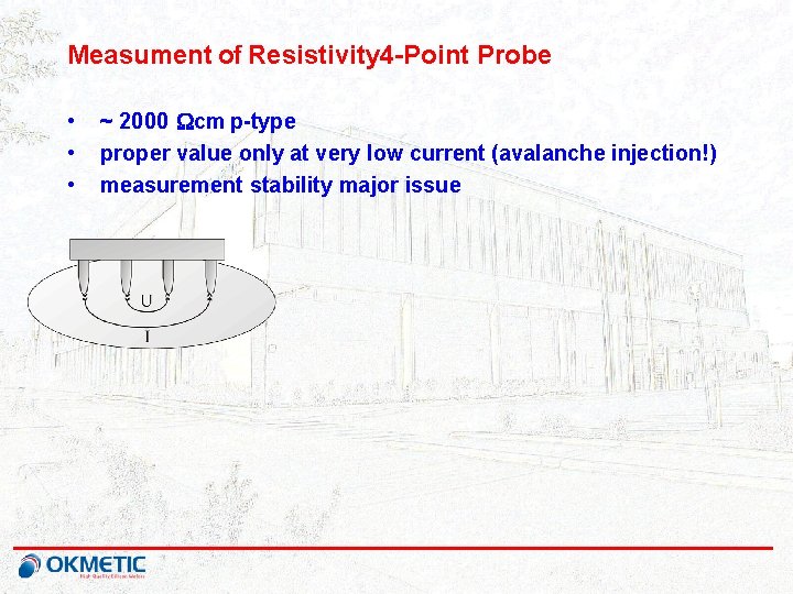
Measument of Resistivity 4 -Point Probe • • • ~ 2000 Wcm p-type proper value only at very low current (avalanche injection!) measurement stability major issue

Manufacture of High Resistivity, Low Oxygen Czochralski Silicon Outline • • Background Crystal growth and wafer manufacturing Wafer characteristics: lifetime and metals High resistivity. CZ • Metals and lifetime • Dopants • Oxygen • Magnetic field • Silicon melt behavior • Conclusions

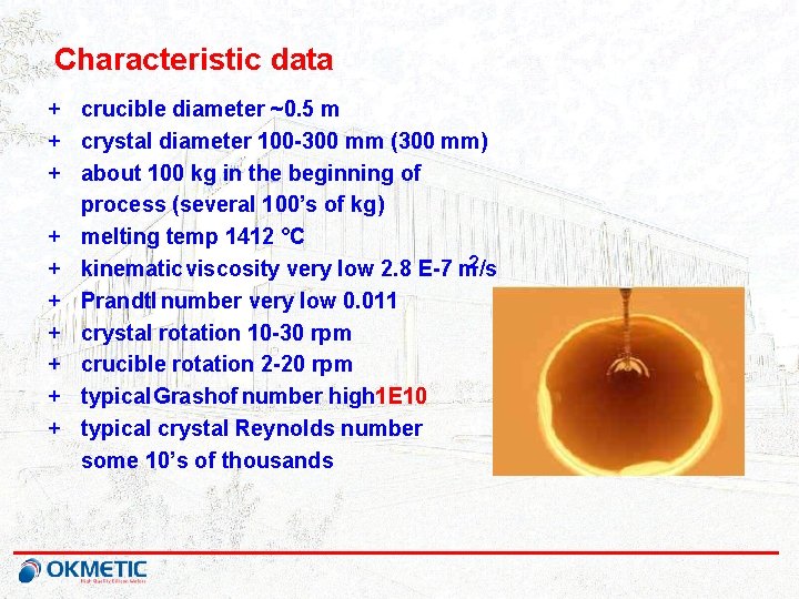
Characteristic data + crucible diameter ~0. 5 m + crystal diameter 100 -300 mm (300 mm) + about 100 kg in the beginning of process (several 100’s of kg) + melting temp 1412 °C + kinematic viscosity very low 2. 8 E-7 m 2/s + Prandtl number very low 0. 011 + crystal rotation 10 -30 rpm + crucible rotation 2 -20 rpm + typical Grashof number high 1 E 10 + typical crystal Reynolds number some 10’s of thousands

Magnetic field effect • Strongest field at crucible corner • flow suppressed by strong field => growth effectively from smaller, less unstable melt • under crystal, minor impact dopant, oxygen distribution is not uniform even with MCZ Melt flow is buoyancy driven turbulent

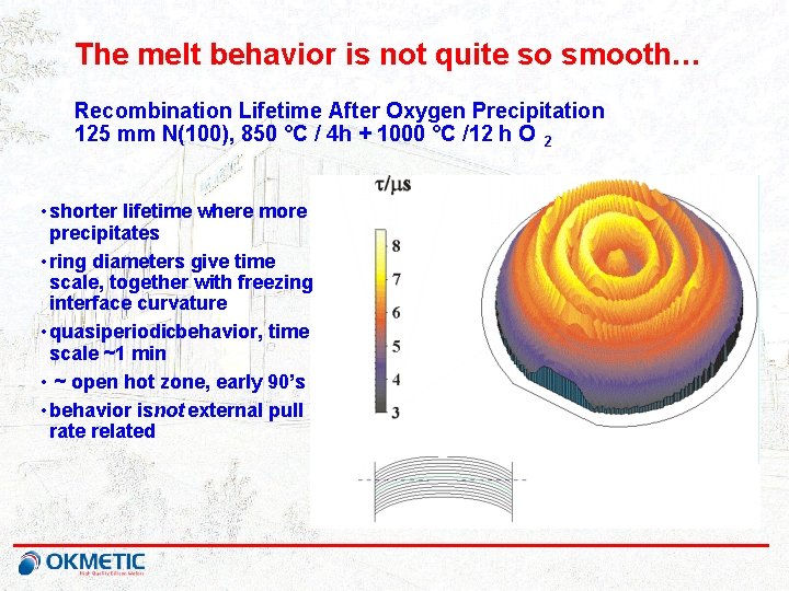
The melt behavior is not quite so smooth… Recombination Lifetime After Oxygen Precipitation 125 mm N(100), 850 °C / 4 h + 1000 °C /12 h O 2 • shorter lifetime where more precipitates • ring diameters give time scale, together with freezing interface curvature • quasiperiodicbehavior, time scale ~1 min • ~ open hot zone, early 90’s • behavior is not external pull rate related

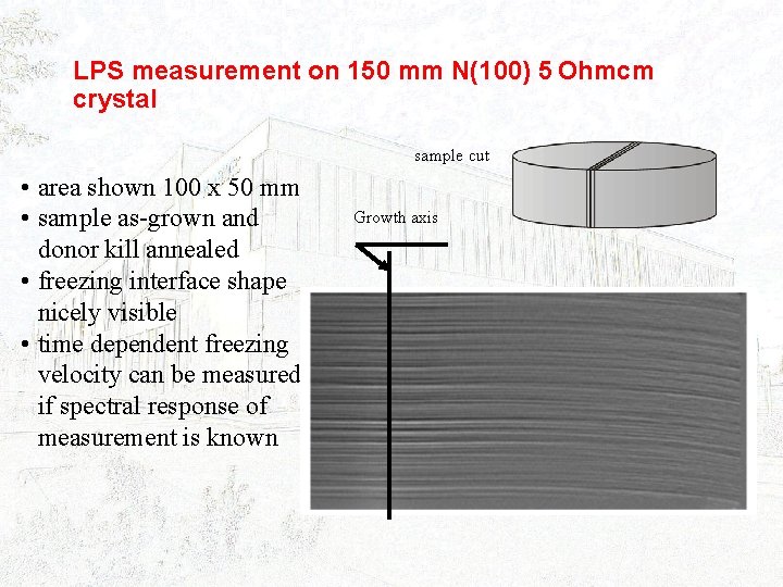
LPS measurement on 150 mm N(100) 5 Ohmcm crystal sample cut • area shown 100 x 50 mm • sample as-grown and donor kill annealed • freezing interface shape nicely visible • time dependent freezing velocity can be measured if spectral response of measurement is known Growth axis

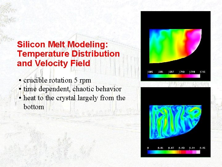
Silicon Melt Modeling: Temperature Distribution and Velocity Field • crucible rotation 5 rpm • time dependent, chaotic behavior • heat to the crystal largely from the bottom

Turbulence It was at a meeting of the British Association in London in 1932 that I remember Hoarce Lamb remarked: “I am an old man now, and when I die and go to Heaven there are two matters on which I hope for enlightenment. One is quantum electrodynamics, and the other is the turbulent motion of fluids. And about the former I am really rather optimistic. ” – Sir Sydney Goldstein Annual Reviews of Fluid Mechanics, Vol. 1 (1969), p. 1

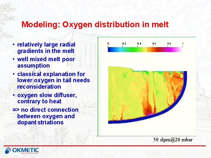
Modeling: Oxygen distribution in melt • relatively large radial gradients in the melt • well mixed melt poor assumption • classical explanation for lower oxygen in tail needs reconsideration • oxygen slow diffuser, contrary to heat => no direct connection between oxygen and dopant striations 50 slpm@20 mbar

Conclusions • Main issues in highresistivity. CZ material • • metallic contamination lifetime dopant level oxygen level have been solved to satisfactory / reasonable level • magnetic Cz and tight control ofdopant contamination mandatory • naturally appearing oxygen offers some advantages • ample space for further developments

Manufacture of High Resistivity, Low Oxygen Czochralski Silicon June 2005 Olli Anttila Okmetic Fellow, Okmetic Oyj