PGA vs LGA Pin Grid Array VS Land


 AM 3+ (942 pin)")


 • CPU MCH Memory 간의 전송 대역폭 • 듀얼코어(775소켓)의 경우")
 • 8 bits(62 pin)/16 bits(98 pin) 병렬 버스 •")


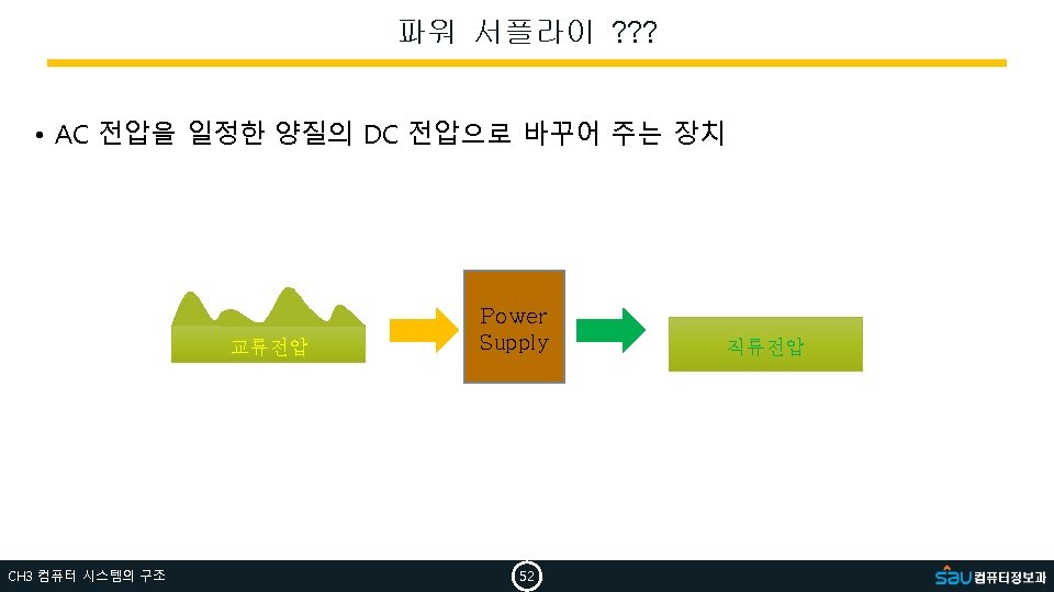
 • PC에서 3차원 그래픽 표현을 빠르게 구현할 수 있게")


- Slides: 58
PGA vs LGA Pin Grid Array VS. Land Grid Arry 출처: wikipedia CH 3 컴퓨터 시스템의 구조 4
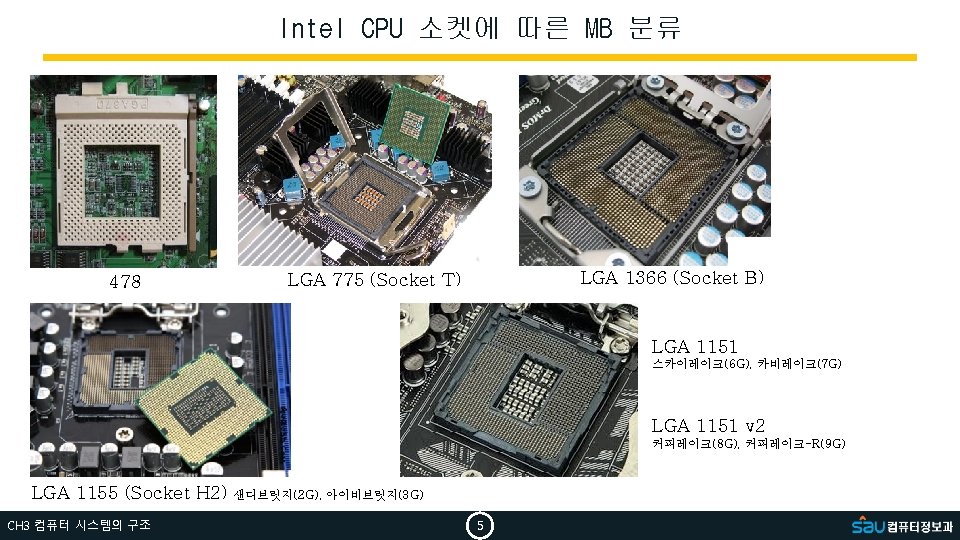
AMD CPU 소켓에 따른 MB 분류 AM 3 (941 pin) AM 3+ (942 pin) AM 4 (1331 pin) Ryzen 시리즈 TR 4 (LGA 4094 pin) Ryzen Threadripper CH 3 컴퓨터 시스템의 구조 6
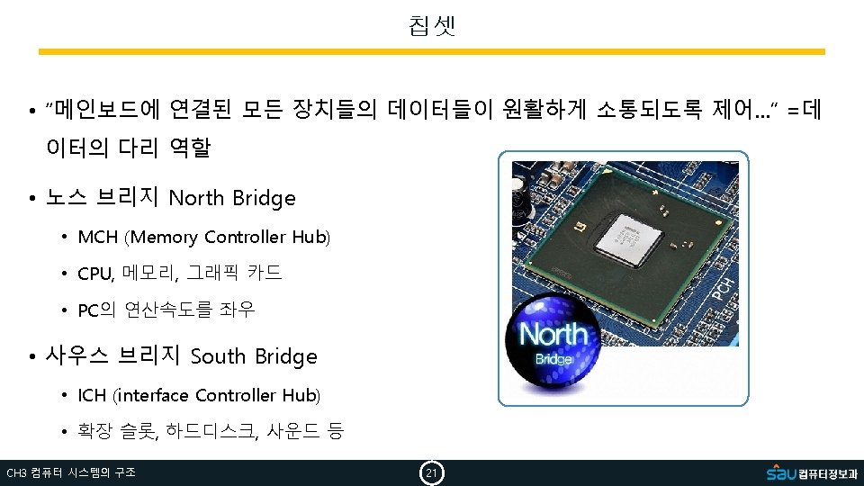
전형적인 칩셋의 위치 North Bridge South Bridge 890 FX CH 3 컴퓨터 시스템의 구조 22
칩셋의 위치 변화 North Bridge South Bridge PCH X 58 CH 3 컴퓨터 시스템의 구조 H 55 23
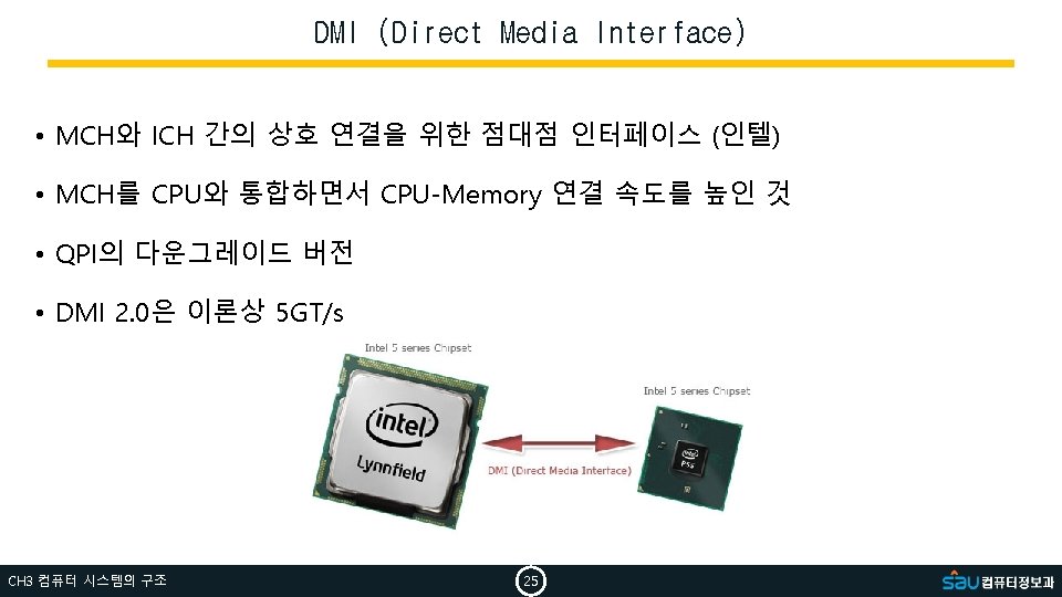
FSB (Front Side Bus) • CPU MCH Memory 간의 전송 대역폭 • 듀얼코어(775소켓)의 경우 • FSB=1, 333 MB/s = 10, 664 Mbps • 즉, PC-10600 RAM을 설치해야 병목현상이 없다. CPU 800 MHz 400 MHz PC 3200 DDR SDRAM CH 3 컴퓨터 시스템의 구조 24
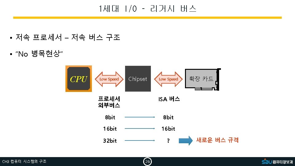
ISA (industry Standard Architecture Bus) • 8 bits(62 pin)/16 bits(98 pin) 병렬 버스 • 5 V, 12 V CH 3 컴퓨터 시스템의 구조 27
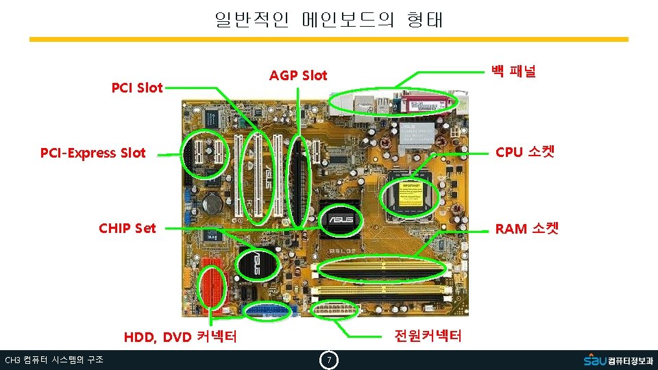
South. Bridge의 등장 CPU 프로세서 버스 Northbridge PCI AGP Memory 버스 Memory Southbridge Local 버스 (High Speed) VGA CH 3 컴퓨터 시스템의 구조 L 2 Cache SCSI LAN 29 Legacy Bus Low Speed Devices
3세대 I/O – Hub Architechture CPU VGA AGP 버스 Northbridge Memory 버스 ATA PCI 버스 Southbridge USB LAN Legacy PC I/O CH 3 컴퓨터 시스템의 구조 30 Memory
4대세 Chipset VGA PCI-2 x 16 버스 CPU Memory 버스 DMI ATA PCI-e 버스 PCH USB LAN Legacy PC I/O CH 3 컴퓨터 시스템의 구조 31 Memory
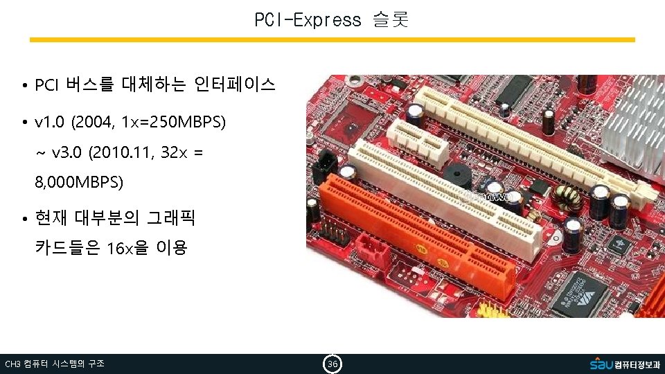
AGP 슬롯 (Accelerated Graphics Port) • PC에서 3차원 그래픽 표현을 빠르게 구현할 수 있게 해주는 버스 규격 • AGP 1 x : 32 bits x 66 MHz = 2112 Mbps ≒ 266 MBPS AGP 8 x : 32 bits x 66 MHz x 8 ≒ 2, 133 MBPS CH 3 컴퓨터 시스템의 구조 35
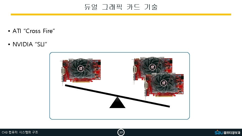
Example of Dual Graphic Card CH 3 컴퓨터 시스템의 구조 40
고성능 SATA 3 지원 • H 67의 경우, SATA 3 x 2대, SATA 2 x 4대 S-ATA (1 bit) P-ATA (16 bits) or E-IDE • 100, 133 MBPS • 80 pins (40 pins 사용) • 8 pins (4 pin 사용) • 8 b/10 b encoding • v 1. 0: 1. 5 Gbps 1. 2 Gbps 150 MBPS • v 2. 0: 3. 0 Gbps 2. 4 Gbps 300 MBPS • v 3. 0: 6. 0 Gbps 4. 8 Gbps 600 MBPS CH 3 컴퓨터 시스템의 구조 43
인텔 9 시리즈 • 인텔 8 시리즈는 Haswell 지원 • 인텔 9 시리즈는 Haswell + Broadwell 지원 PCI Express M. 2 SATA Express 이론상 10 Gbps CH 3 컴퓨터 시스템의 구조 Page 45
네트워크 칩 리얼텍社 RTL 8111 E Gbit Ethernet CH 3 컴퓨터 시스템의 구조 Intel社 WG 82579 V Gbit Ethernet 49 Marvell社 88 E 8071 -NNC 1 Gbit Ethernet
Thank you for watching CH 3 컴퓨터 시스템의 구조 58