8086 Ahad 2 Internal External 8086 vs 8088
![8086 Ahad [2] 8086 Ahad [2]](https://slidetodoc.com/presentation_image/0f2b0c8fa2b2390b837dfe676c009b3c/image-1.jpg)


![HOLD (input , Active High) : it requests a DMA [Direct Memory Access] 1 HOLD (input , Active High) : it requests a DMA [Direct Memory Access] 1](https://slidetodoc.com/presentation_image/0f2b0c8fa2b2390b837dfe676c009b3c/image-23.jpg)
- Slides: 36
![8086 Ahad 2 8086 Ahad [2]](https://slidetodoc.com/presentation_image/0f2b0c8fa2b2390b837dfe676c009b3c/image-1.jpg)
8086 Ahad [2]

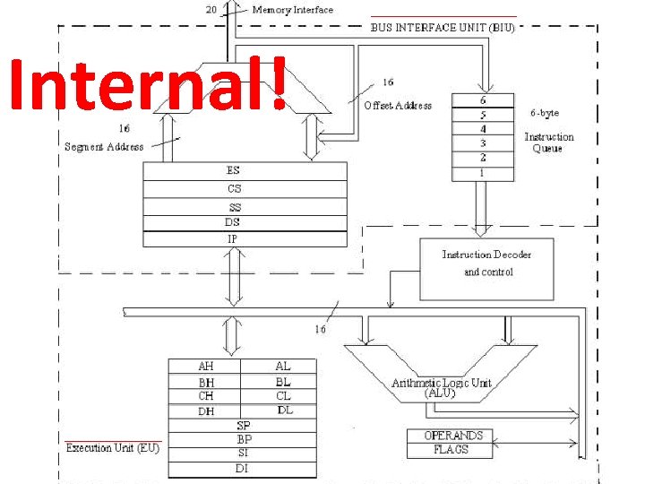
Internal!

External?

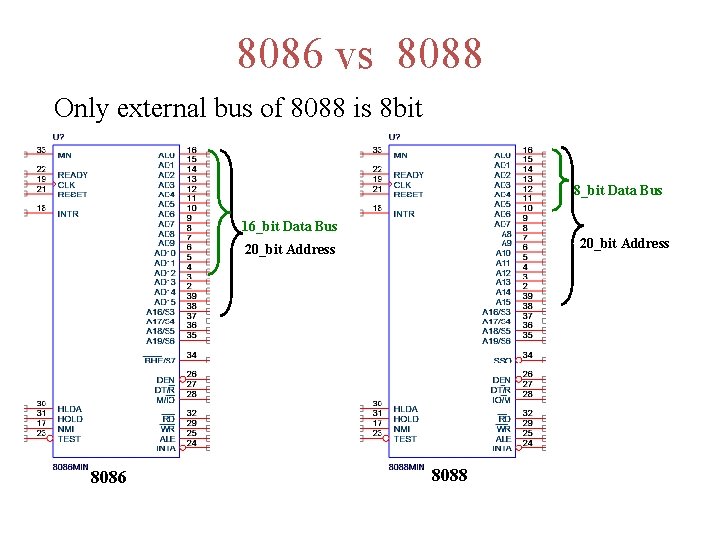
8086 vs 8088 Only external bus of 8088 is 8 bit 8_bit Data Bus 16_bit Data Bus 20_bit Address 8086 8088

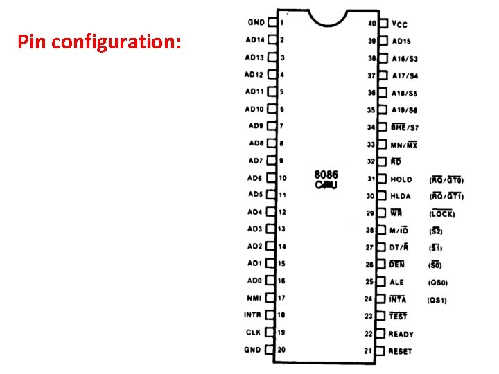
Pin configuration:

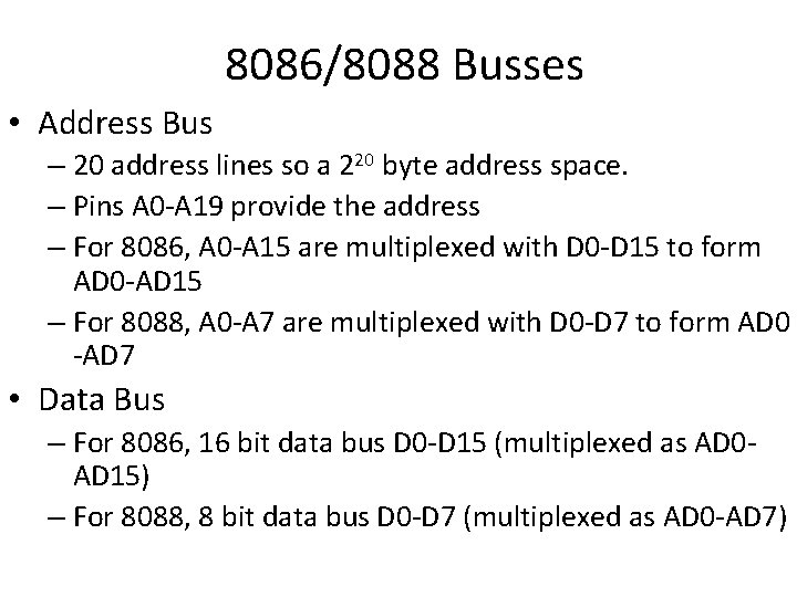
8086/8088 Busses • Address Bus – 20 address lines so a 220 byte address space. – Pins A 0 -A 19 provide the address – For 8086, A 0 -A 15 are multiplexed with D 0 -D 15 to form AD 0 -AD 15 – For 8088, A 0 -A 7 are multiplexed with D 0 -D 7 to form AD 0 -AD 7 • Data Bus – For 8086, 16 bit data bus D 0 -D 15 (multiplexed as AD 0 AD 15) – For 8088, 8 bit data bus D 0 -D 7 (multiplexed as AD 0 -AD 7)

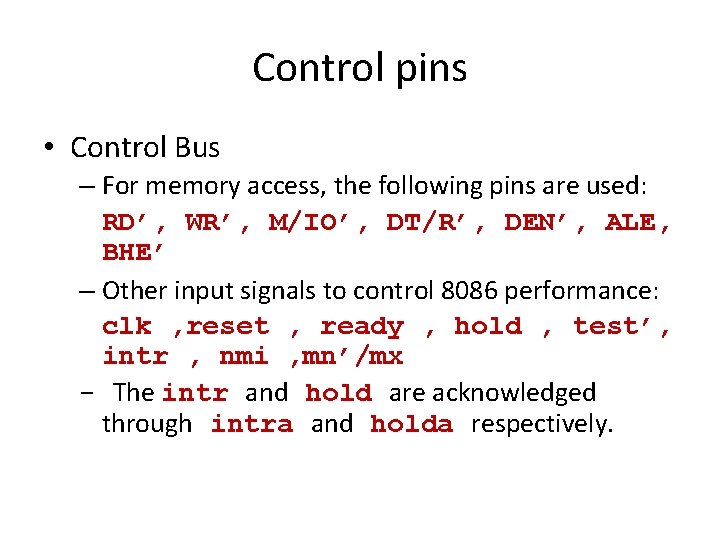
Control pins • Control Bus – For memory access, the following pins are used: RD’, WR’, M/IO’, DT/R’, DEN’, ALE, BHE’ – Other input signals to control 8086 performance: clk , reset , ready , hold , test’, intr , nmi , mn’/mx - The intr and hold are acknowledged through intra and holda respectively.

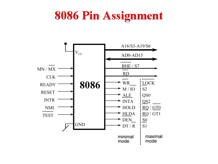
8086 Pin Assignment

8086 Pin Description Vcc (pin 40) : Power supply input GND (pin 1 and 20) : Ground pin is the return of the power supply

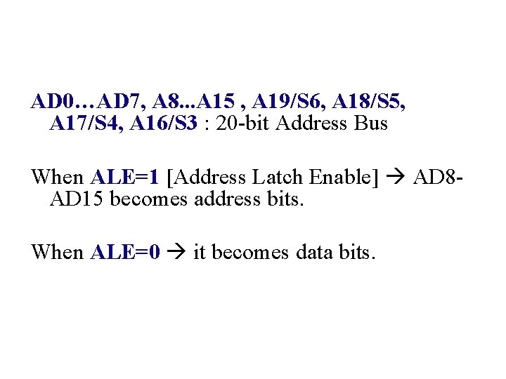
AD 0…AD 7, A 8. . . A 15 , A 19/S 6, A 18/S 5, A 17/S 4, A 16/S 3 : 20 -bit Address Bus When ALE=1 [Address Latch Enable] AD 8 AD 15 becomes address bits. When ALE=0 it becomes data bits.

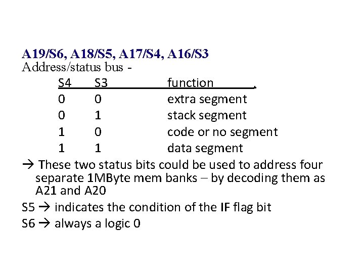
A 19/S 6, A 18/S 5, A 17/S 4, A 16/S 3 Address/status bus S 4 S 3 function . 0 0 extra segment 0 1 stack segment 1 0 code or no segment 1 1 data segment These two status bits could be used to address four separate 1 MByte mem banks – by decoding them as A 21 and A 20 S 5 indicates the condition of the IF flag bit S 6 always a logic 0

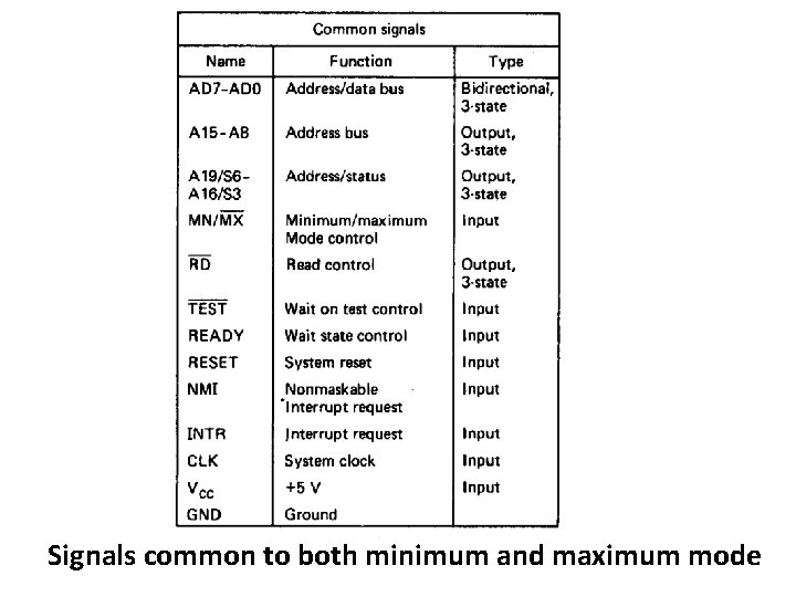
MN/MX’ (33, input) : Indicates Operating mode – min mode or max mode

READY (input, Active High) : Takes µP to wait state 0 µP enters into wait states n remains idle. 1 no effect on the operation of the µP

CLK (input) : Provides basic timing for the processor CLK must have a duty cycle of 33% (high for 1/3 of the clocking period & low for 2/3)

DEN’ (output) : activates external data bus buffers. It is LOW when processor wants to receive data or processor is giving out data

DT/R’ (output) : Data Transmit/Receive. 1 data from µP to memory 0 data is from memory to µP

M/IO’ (output) : selects mem or I/O. It indicates that the m. P address bus contains – either a memory address or an I/O port address. 1 µP access I/O Device 0 µP access memory

RD’ (output) : When Low, µP is performing a read operation 0 the data bus is receptive to data from the mem or I/O devices connected to the system.

WR’ (output) : When Low, µP is performing a write operation It is outputting data to a mem or I/O device. During the time WR=0, the data bus contains a valid data for mem or I/O.

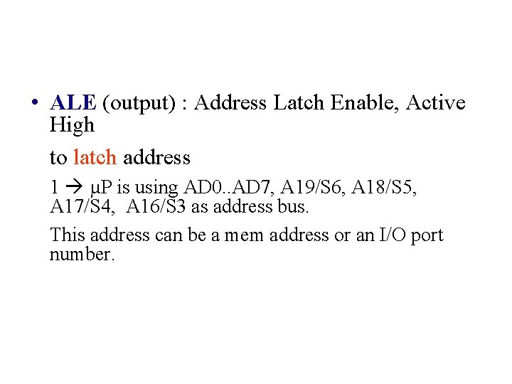
• ALE (output) : Address Latch Enable, Active High to latch address 1 µP is using AD 0. . AD 7, A 19/S 6, A 18/S 5, A 17/S 4, A 16/S 3 as address bus. This address can be a mem address or an I/O port number.

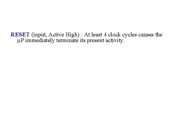
RESET (input, Active High) : At least 4 clock cycles causes the µP immediately terminate its present activity.

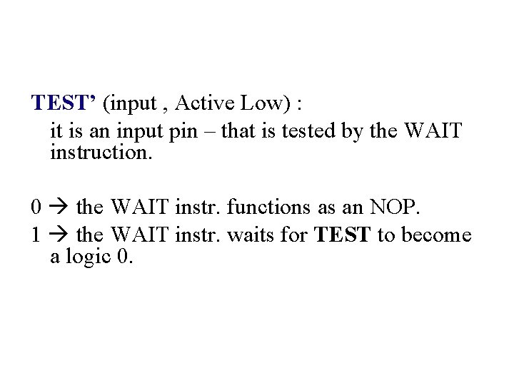
TEST’ (input , Active Low) : it is an input pin – that is tested by the WAIT instruction. 0 the WAIT instr. functions as an NOP. 1 the WAIT instr. waits for TEST to become a logic 0.
![HOLD input Active High it requests a DMA Direct Memory Access 1 HOLD (input , Active High) : it requests a DMA [Direct Memory Access] 1](https://slidetodoc.com/presentation_image/0f2b0c8fa2b2390b837dfe676c009b3c/image-23.jpg)
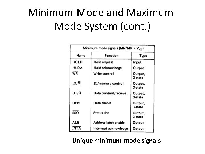
HOLD (input , Active High) : it requests a DMA [Direct Memory Access] 1 the m. P stops executing software and places its address, data, and control bus at the high-impedance state. 0 m. P executes SW normally.

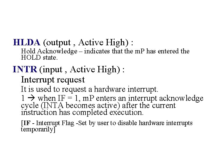
HLDA (output , Active High) : Hold Acknowledge – indicates that the m. P has entered the HOLD state. INTR (input , Active High) : Interrupt request It is used to request a hardware interrupt. 1 when IF = 1, m. P enters an interrupt acknowledge cycle (INTA becomes active) after the current instruction has completed execution. [IF - Interrupt Flag -Set by user to disable hardware interrupts temporarily]

INTA’ (output , Active Low) : Interrupt Acknowledge NMI (input , Active High) : Non-maskable interrupt similar to INTR – except that the NMI interrupt does not check to see whether the IF flag is 1.

• The AD 0 -AD 15 lines are a 16 -bit multiplexed addressed or data bus. • During the 1 st clock cycle, AD 0 -AD 15 are the low order 16 -bit address. • The 8086 has a total of 20 address line, the upper 4 lines are multiplexed with the state signal that is A 16/S 3, A 17/S 4, A 18/S 5, A 19/S 6. • For memory and i/o operations, AD 15 -AD 0 contain the 16 bit data and S 3, S 4, S 5, S 6 become the status line.

• BHE/S 7 is used as best high enable during the 1 st clock cycle of an instruction execution. • BHE can be used in conjunction with AD 0 to select the memory

• RD is low when the data is read from memory or I/O location

• TEST is an input pin and is only used by the wait instruction • 8086 enters a wait state after execution of the wait instruction until a low is seen on the test pin.

• ALE is an address latch enable is an o/p signal provided by the 8086 • - can be used to demultiplexed AD 0 to AD 15 in to A 10 to. A 15 and D 0 to D 15.

• M/IO is an 8086 output signal to distinguish a memory access and i/o access.

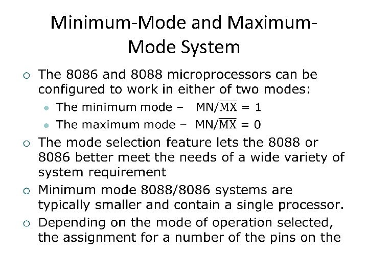
33. MN/MX • The 8086 can operate in two modes: 1. minimum mode and 2. maximum mode For minimum mode, a unique processor system with a single 8086 For maximum mode, a multi-processor system with more than one 8086.

Minimum-Mode and Maximum. Mode System •

Signals common to both minimum and maximum mode

Minimum-Mode and Maximum. Mode System (cont. ) Unique minimum-mode signals

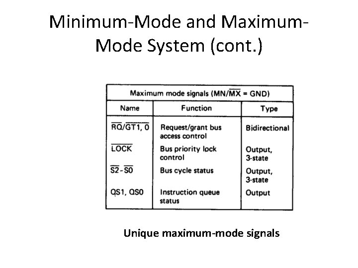
Minimum-Mode and Maximum. Mode System (cont. ) Unique maximum-mode signals