UNIT 1 The 8051 Microcontroller Architecture Pin Diagram


 is")

 • 6 interrupt")
: - it is used for data transfer and")

: - This is an 8 bit register.")
: - DPTR is a 16 bit register. It consists of higher")


 • One of the most useful features of the 8051")

 Internal CPU")


: Program Store Enable, the read signal for external program")
: – Vcc provides supply voltage to the chip.")


 XTAL = 11. 0592 MHz (b)")
:reset – input pin and active high(normally low). •")


:external access – There is no on-chip ROM in")
:address latch enable – It is an output pin")


 is given")


![Structure of Assembly Language [ label: ] mnemonic [operands] [ ; comment ] Example:](https://slidetodoc.com/presentation_image_h/23e4c8e86562900d83567f1ca0533b74/image-53.jpg "Structure of Assembly Language [ label: ] mnemonic [operands] [ ; comment ] Example:")


 and a")


 by")


 register q. All interrupt are disabled after reset q. We can")


 Register --- PT 2 PS PT 1 PX 1 PT 0")


 XTAL = 11. 0592 MHz (b)")


 GATE C/T M 1 Timer 1 Functions of individual bits of TMOD M")
 1 : Counter")


 TF 1 TR 1 TF 0 TR 0 Timer 1 Timer")


 • This is same for timer")
 (5 bits)")


 • This is the most commonly")


 • When a timer is in")


 � When Timer 0 is placed in mode")
 fosc C/T")

")


 TH 0 -TL")
 overflow flag Timer 0 external input Pin")


 - Fast, but distance cannot be great.")
 • P/S: Parallel-in-Serial-out Shift Register • S/P:")

")

 transmissions.")
 8 -bit - When")

 is also")
, COM 2: (MODEM & RS 232) •")


 or")

 TH 1")
 1. MOV TMOD, #20 H ; Timer 1, mode 2 2. TH")
 1. MOV TMOD, #20 H ; Timer 1, mode 2 2. TH")
- Slides: 164
UNIT 1 The 8051 Microcontroller • Architecture • Pin Diagram • Special function Registers • Operation of I/O Ports • Addressing Modes • Instruction set
General-purpose microprocessor: • CPU for Computers • Commonly no RAM, ROM, I/O on CPU chip itself CPU General. Purpose Microprocessor Many chips on motherboard Data Bus RAM ROM I/O Port Timer Serial COM Port Address Bus 2
Microcontroller • A single-chip computer • On-chip RAM, ROM, I/O ports. . . • Example:Motorola’s 6811, Intel’s 8051, Zilog’s Z 8 and PIC 16 X CPU I/O Port RAM ROM Serial Timer COM Port A single chip Microcontroller ACOE 343 - Real-Time Embedded Processor Systems - Frederick University 3
Microprocessor vs. Microcontroller Microprocessor Microcontroller • CPU is stand-alone, RAM, ROM, • I/O, timer are separate • Designer can decide on the amount • of ROM, RAM and I/O ports. • Expensive • • general-purpose • High processing power • • High power consumption • Instruction sets focus on processing- • intensive operations • • Typically 32/64 – bit • • Typically deep pipeline (5 -20 stages) • CPU, RAM, ROM, I/O and timer are all on a single chip fixed amount of on-chip ROM, RAM, I/O ports for applications in which cost, power and space are critical single-purpose (control-oriented) Low processing power Low power consumption Bit-level operations Instruction sets focus on control and bit-level operations • Typically 8/16 bit • Typically single-cycle/two-stage pipeline 4
What is Microcontroller? • A microcontroller (sometimes abbreviated µC, u. C or MCU) is a small computer on a single integrated circuit containing a processor core, memory, and programmable input/output peripherals. • Microcontrollers are designed for embedded applications, in contrast to the microprocessors used in personal computers or other general purpose applications. • Microcontrollers are used in automatically controlled products and devices, such as automobile engine control systems, implantable medical devices, remote controls, office machines, appliances, power tools, toys and other embedded systems.
80 C 51 Block Diagram 6
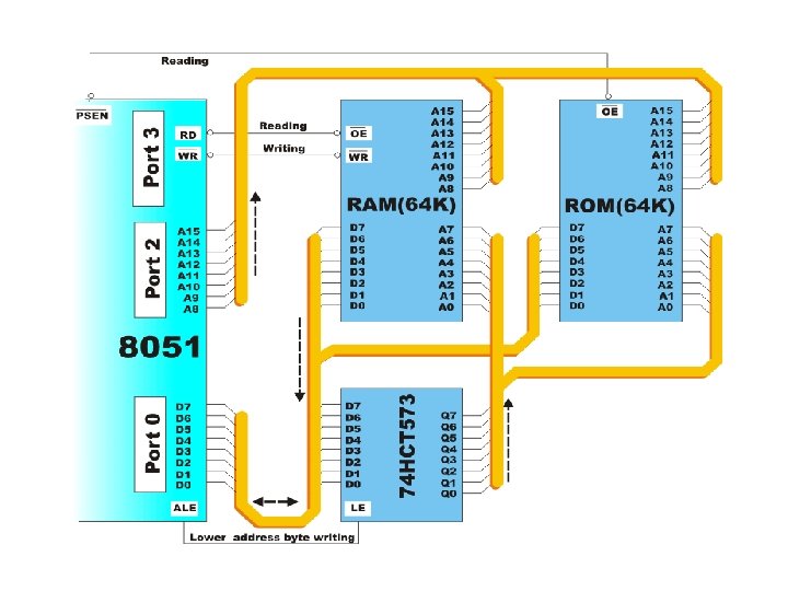
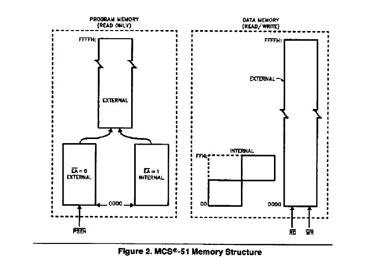
Other 8051 featurs • only 1 On chip oscillator (external crystal) • 6 interrupt sources (2 external , 3 internal, Reset) • 64 K external code (program) memory(only read)PSEN • 64 K external data memory(can be read and write) by RD, WR • Code memory is selectable by EA (internal or external) • We may have External memory as data and code
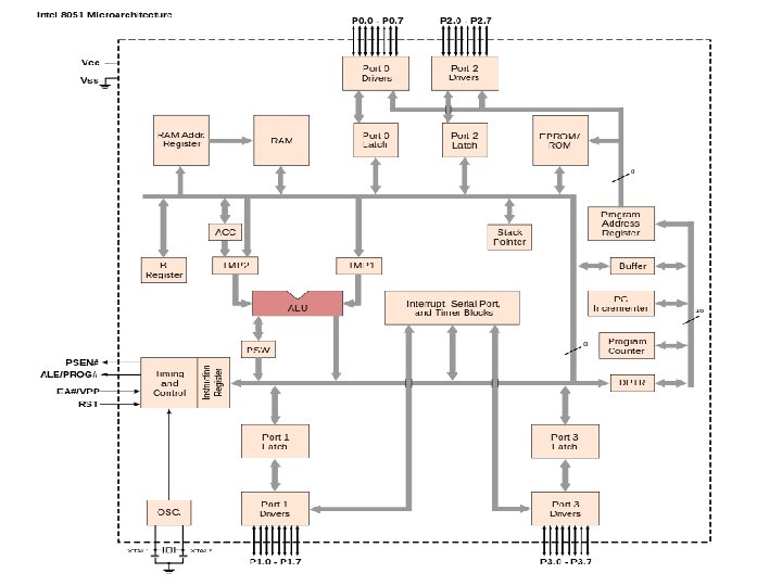
Operation of each block: • ACCUMULATOR(ACC): - it is used for data transfer and arithmetic operations. After any operation result is stored in ACC and can be accessed through its SFR address of 0 E 0 H. • B REGISTER: - it is used to store the upper 8 bit result of multiplication and divisions. It is used as temporary register and can be accessed through its SFR address of 0 F 0 H.
Operation of each block: CY AC FO RS 1 RS 0 OV P • PROGRAM STATUS WORD(PSW): - This special function register and consists of different status bits that reflect the current state of microcontroller. It contains carry (CY), the auxiliary carry(AC), the two registors bank select bits(RS 1 and RS 0), the overflow flag(OV), a parity bit(P), and two user defined status flags.
Operation of each block: � STACK POINTER(SP): - This is an 8 bit register. SP is incremented before the data is stored onto the stack using PUSH/CALL instructions execution. During PUSH, first SP is incremented and then copy the data. In the POP operation, initially copy the data and then decrement the SP.
� DATA POINTER(DTPR): - DPTR is a 16 bit register. It consists of higher byte (DPH) and a lower byte (DPL). DPTR is very useful for string operations and look up table operations. With a 16 bit DPTR, a maximum of 64 K of off chip data memory and 64 k of off chip memory can be addressed.
Operation of each block: PORT 0, PORT 1, PORT 2, PORT 3 LATCHES AND DRIVERS: - Each latch and corresponding drivers of port 0 -3 is allotted to the corresponding on chip I/O port.
8051 Schematic Pin out
8051 Foot Print P 1. 0 P 1. 1 P 1. 2 P 1. 3 P 1. 4 P 1. 5 P 1. 6 P 1. 7 RST (RXD)P 3. 0 (TXD)P 3. 1 (INT 0)P 3. 2 (INT 1)P 3. 3 (T 0)P 3. 4 (T 1)P 3. 5 (WR)P 3. 6 (RD)P 3. 7 XTAL 2 XTAL 1 GND 1 2 3 4 5 6 7 8 9 10 11 12 13 14 15 16 17 18 19 20 8051 (8031) (8751) (8951) 40 39 38 37 36 35 34 33 32 31 30 29 28 27 26 25 24 23 22 21 Vcc P 0. 0(AD 0 )P 0. 1(AD 1) P 0. 2(AD 2 ) 0. 3(AD 3) P P 0. 4(AD 4) P 0. 5(AD 5) P 0. 6(AD 6) P 0. 7(AD 7) EA/VPP ALE/PROG PSEN P 2. 7(A 15) P 2. 6(A 14) P 2. 5(A 13) P 2. 4(A 12) P 2. 3(A 11) P 2. 2(A 10) P 2. 1(A 9) P 2. 0(A 8)
IMPORTANT PINS (IO Ports) • One of the most useful features of the 8051 is that it contains four I/O ports (P 0 - P 3) • Port 0 (pins 32 -39):P 0(P 0. 0~P 0. 7) – 8 -bit R/W - General Purpose I/O – Or acts as a multiplexed low byte address and data bus for external memory design • Port 1 (pins 1 -8) :P 1(P 1. 0~P 1. 7) – Only 8 -bit R/W - General Purpose I/O • Port 2 (pins 21 -28):P 2(P 2. 0~P 2. 7) – 8 -bit R/W - General Purpose I/O – Or high byte of the address bus for external memory design • Port 3 (pins 10 -17):P 3(P 3. 0~P 3. 7) – General Purpose I/O – if not using any of the internal peripherals (timers) or external interrupts. • Each port can be used as input or output (bi-direction)
Port 3 Alternate Functions
Hardware Structure of I/O Pin Read latch TB 2 Vcc Load(L 1) Internal CPU bus D Write to latch Clk P 1. X pin Q P 1. X M 1 Q TB 1 Read pin
Hardware Structure of I/O Pin • Each pin of I/O ports – Internally connected to CPU bus – A D latch store the value of this pin • Write to latch= 1:write data into the D latch – 2 Tri-state buffer: • TB 1: controlled by “Read pin” – Read pin= 1:really read the data present at the pin • TB 2: controlled by “Read latch” – Read latch= 1:read value from internal latch – A transistor M 1 gate • Gate=0: open • Gate=1: close
Writing “ 1” to Output Pin P 1. X Read latch Vcc TB 2 1. write a 1 to the pin Internal CPU bus D Write to latch Clk Q Load(L 1) 1 0 TB 1 Read pin P 1. X Q 2. output pin is Vcc M 1 output 1
Writing “ 0” to Output Pin P 1. X Read latch Vcc TB 2 1. write a 0 to the pin Internal CPU bus D Write to latch Clk Q Load(L 1) 0 1 TB 1 Read pin P 1. X Q 2. output pin is ground M 1 output 0
Reading “High” at Input Pin Read latch 2. MOV A, P 1 Vcc TB 2 external pin=High Load(L 1) Internal CPU bus D Q 1 1 P 1. X Write to latch Clk Q 0 M 1 TB 1 Read pin 3. Read pin=1 Read latch=0 Write to latch=1 8051 IC P 1. X pin
Reading “Low” at Input Pin Read latch Vcc 2. MOV A, P 1 TB 2 Load(L 1) Internal CPU bus D Q 0 0 P 1. X Write to latch Clk Q 1 M 1 TB 1 Read pin 3. Read pin=1 Read latch=0 Write to latch=1 8051 IC external pin=Low P 1. X pin
Port 0 with Pull-Up Resistors Vcc Port 0 8751 8951 8051 P 0. 0 P 0. 1 P 0. 2 P 0. 3 P 0. 4 P 0. 5 P 0. 6 P 0. 7 10 K
IMPORTANT PINS • PSEN (out): Program Store Enable, the read signal for external program memory (active low). • ALE (out): Address Latch Enable, to latch address outputs at Port 0 and Port 2 • EA (in): External Access Enable, active low to access external program memory locations 0 to 4 K • • RXD, TXD: UART pins for serial I/O on Port 3 XTAL 1 & XTAL 2: Crystal inputs for internal oscillator.
Pins of 8051 • Vcc(pin 40): – Vcc provides supply voltage to the chip. – The voltage source is +5 V. • GND(pin 20):ground • XTAL 1 and XTAL 2(pins 19, 18): – These 2 pins provide external clock. – Way 1:using a quartz crystal oscillator – Way 2:using a TTL oscillator
XTAL Connection to 8051 • Using a quartz crystal oscillator • We can observe the frequency on the XTAL 2 C 2 pin. XTAL 2 30 p. F C 1 XTAL 1 30 p. F GND
XTAL Connection to an External Clock Source • Using a TTL oscillator • XTAL 2 is unconnected. N C EXTERNAL OSCILLATOR SIGNAL XTAL 2 XTAL 1 GND
Machine cycle Find the machine cycle for (a) XTAL = 11. 0592 MHz (b) XTAL = 16 MHz. Solution: (a) 11. 0592 MHz / 12 = 921. 6 k. Hz; machine cycle = 1 / 921. 6 k. Hz = 1. 085 s (b) 16 MHz / 12 = 1. 333 MHz; machine cycle = 1 / 1. 333 MHz = 0. 75 s
Pins of 8051 • RST(pin 9):reset – input pin and active high(normally low). • The high pulse must be high at least 2 machine cycles. – power-on reset. • Upon applying a high pulse to RST, the microcontroller will reset and all values in registers will be lost. • Reset values of some 8051 registers – power-on reset circuit
Power-On RESET Vcc 31 10 u. F 30 p. F 9 8. 2 K EA/VPP X 1 X 2 RST
RESET Value of Some 8051 Registers: Register Reset Value PC 0000 ACC 0000 B 0000 PSW 0000 SP 0007 DPTR 0000 RAM are all zero
Pins of 8051 • /EA(pin 31):external access – There is no on-chip ROM in 8031 and 8032. – The /EA pin is connected to GND to indicate the code is stored externally. – /PSEN & ALE are used for external ROM. – For 8051, /EA pin is connected to Vcc. – “/” means active low. • /PSEN(pin 29):program store enable – This is an output pin and is connected to the OE pin of the ROM.
Pins of 8051 • ALE(pin 30):address latch enable – It is an output pin and is active high. – 8051 port 0 provides both address and data.
On-Chip Memory Internal RAM
Registers 1 F Bank 3 18 17 Bank 2 10 0 F Bank 1 08 07 06 05 04 03 02 01 00 R 7 R 6 R 5 R 4 R 3 R 2 R 1 R 0 Bank 0 Four Register Banks Each bank has R 0 -R 7 Selectable by psw. 2, 3
Bit Addressable RAM Figure 2 -6 Summary of the 8051 on -chip data memory (RAM)
Bit Addressable RAM Figure 2 -6 Summary of the 8051 on -chip data memory (Special Function Registers)
Addressing modes What is an addressing mode ? • Addressing mode is a way to address an operand. Operand means the data we are operating upon (in most cases source data). It can be a direct address of memory, it can be register names, it can be any numerical data etc. e. g with a simple data move instruction of 8051. MOV A, #6 AH • Here the data 6 A is the operand, often known as source data. When this instruction is executed, the data 6 AH is moved to accumulator A. There are 5 different ways to execute this instruction and hence we say, we have got 5 addressing modes for 8051. They are 1) Immediate addressing mode 2) Direct addressing mode 3) Register direct addressing mode 4) Register indirect addressing mode 5) Indexed addressing mode.
Immediate addressing mode MOV A, #6 AH In general we can write MOV A, #data This addressing mode is named as “immediate” because it transfers an 8 -bit data immediately to the accumulator (destination operand).
Note: The ‘#’ symbol before 6 AH indicates that operand is a data (8 bit). If ‘#’ is not present then the hexadecimal number would be taken as address.
Direct addressing mode Here the address of the data (source data ) is given as operand. Lets take an example. MOV A, 04 H Here 04 H is the address of register 4 of register bank#0. When this instruction is executed, what ever data is stored in register 04 H is moved to accumulator. In the picture below we can see, register 04 H holds the data 1 FH. So the data 1 FH is moved to accumulator.
Note: We have not used ‘#’ in direct addressing mode, unlike immediate mode. If we had used ‘#’, the data value 04 H would have been transferred to accumulator instead 0 f 1 FH.
ØExample: MOV R 0, 40 H // save content of RAM location 40 h into R 0. MOV 56 H, A // save content of A in RAM location 56 H.
Register direct addressing mode • In this addressing mode we use the register name directly (as source operand). An example is shown below. MOV A, R 4 In register direct addressing mode, data is transferred to accumulator from the register (based on which register bank is selected).
Also note that the instruction above is 1 byte and requires 1 cycle for complete execution. This means using register direct addressing mode can save program memory.
Register indirect addressing mode So in this addressing mode, address of the data (source data to transfer) is given in the register operand. MOV A, @R 0 Here the value inside R 0 is considered as an address, which holds the data to be transferred to accumulator.
This is a single byte instruction and the program counter increments 1 and moves to 0203 of program memory. Note: Only R 0 and R 1 are allowed to form a register indirect addressing instruction. In other words programmer can must make any instruction either using @R 0 or @R 1. All register banks are allowed.
Indexed addressing mode • MOVC A, @A+DPTR and MOVC A, @A+PC where DPTR is data pointer and PC is program counter (both are 16 bit registers). Lets take the first example. • MOVC A, @A+DPTR • What’s the first impression you have now? The source operand is @A+DPTR and we know we will get the source data (to transfer) from this location. It is nothing but adding contents of DPTR with present content of accumulator. This addition will result a new data which is taken as the address of source data (to transfer). The data at this address is then transferred to accumulator.
This is a 1 byte instruction with 2 cycles needed for execution. What you infer from that? The execution time required for this instruction is high compared to previous instructions (which all were 1 cycle). The other example MOVC A, @A+PC works the same way as above example. The only difference is, instead of adding DPTR with accumulator, here data inside program counter (PC) is added with accumulator to obtain the target address.
Structure of Assembly Language [ label: ] mnemonic [operands] [ ; comment ] Example: MOV R 1, #25 H ; load data 25 H into R 1 53
8051 Assembly Language • Registers MOV Instruction: MOV destination, source Example: 1. MOV A, #55 H 2. MOV R 0, A 3. MOV A, R 3 54
Instruction Groups • The 8051 has 255 instructions – Every 8 -bit opcode from 00 to FF is used. • The instructions are grouped into 5 groups – Arithmetic – Logic – Data Transfer – Boolean – Branching
Arithmetic Instructions • ADD – 8 -bit addition between the accumulator (A) and a second operand. • The result is always in the accumulator. • The CY flag is set/reset appropriately. • ADDC – 8 -bit addition between the accumulator, a second operand the previous value of the CY flag. • Useful for 16 -bit addition in two steps. • The CY flag is set/reset appropriately.
Arithmetic Instructions • DA – Decimal adjust the accumulator. • Format the accumulator into a proper 2 digit packed BCD number. • Operates only on the accumulator. • Works only after the ADD instruction. • SUBB – Subtract with Borrow. • Subtract an operand the previous value of the borrow (carry) flag from the accumulator. – A A - <operand> - CY. – The result is always saved in the accumulator. – The CY flag is set/reset appropriately.
Logical Operations • ANL / ORL – Work on byte sized operands or the CY flag. • ANL A, Rn • ANL A, direct • ANL A, @Ri • ANL A, #data • ANL direct, A • ANL direct, #data • ANL C, bit • ANL C, /bit
Data Transfer Instructions • MOV – 8 -bit data transfer for internal RAM and the SFR. • MOV A, Rn MOV A, direct • MOV A, @Ri MOV A, #data • MOV Rn, A MOV Rn, direct • MOV Rn, #data MOV direct, A • MOV direct, Rn. MOV direct, direct • MOV direct, @Ri MOV direct, #data • MOV @Ri, A MOV @Ri, direct • MOV @Ri, #data
Data Transfer Operations • MOV – 1 -bit data transfer involving the CY flag • MOV C, bit • MOV bit, C • MOV – 16 -bit data transfer involving the DPTR • MOV DPTR, #data
Data Transfer Instructions • MOVC – Move Code Byte • Load the accumulator with a byte from program memory. • Must use indexed addressing § MOVC A, @A+DPTR A, @A+PC
Data Transfer Instructions • MOVX – Data transfer between the accumulator and a byte from external data memory. • • MOVX A, @Ri A, @DPTR @Ri, A @DPTR, A
Data Transfer Instructions • PUSH / POP – Push and Pop a data byte onto the stack. – The data byte is identified by a direct address from the internal RAM locations. • PUSH DPL • POP 40 H
Data Transfer Instructions • XCH – Exchange accumulator and a byte variable • XCH A, Rn • XCH A, direct • XCH A, @Ri • XCHD – Exchange lower digit of accumulator with the lower digit of the memory location specified. • XCHD A, @Ri • The lower 4 -bits of the accumulator are exchanged with the lower 4 -bits of the internal memory location identified indirectly by the index register. • The upper 4 -bits of each are not modified.
Boolean Operations • This group of instructions is associated with the single-bit operations of the 8051. • This group allows manipulating the individual bits of bit addressable registers and memory locations as well as the CY flag. – The P, OV, and AC flags cannot be directly altered. • This group includes: – Set, clear, and, or complement, move. – Conditional jumps.
Boolean Operations • CLR – Clear a bit or the CY flag. • CLR P 1. 1 • CLR C • SETB – Set a bit or the CY flag. • SETB A. 2 • SETB C • CPL – Complement a bit or the CY flag. • CPL 40 H ; Complement bit 40 of the bit addressable memory
Boolean Operations • ORL / ANL – OR / AND a bit with the CY flag. • ORL C, 20 H ; OR bit 20 of bit addressable with the CY flag ; memory • ANL C, /34 H ; AND complement of bit 34 of bit addressable memory with the CY flag. • MOV – Data transfer between a bit and the CY flag. • MOV C, 3 FH ; Copy the CY flag to bit 3 F of the memory. • MOV P 1. 2, C ; Copy the CY flag to bit 2 of P 1. bit addressable
Boolean Operations • JC / JNC – Jump to a relative address if CY is set / cleared. • JB / JNB – Jump to a relative address if a bit is set / cleared. • JB ACC. 2, <label> • JBC – Jump to a relative address if a bit is set and clear the bit.
Branching Instructions • The 8051 provides four different types of unconditional jump instructions: – Short Jump – SJMP • Uses an 8 -bit signed offset relative to the 1 st byte of the next instruction. – Long Jump – LJMP • Uses a 16 -bit address. • 3 byte instruction capable of referencing any location in the entire 64 K of program memory.
Branching Instructions • Compare and Jump if Not Equal – CJNE – Compare the magnitude of the two operands and jump if they are not equal. • The values are considered to be unsigned. • The Carry flag is set / cleared appropriately. § § CJNE A, direct, rel A, #data, rel Rn, #data, rel @Ri, #data, rel
Branching Instructions • Decrement and Jump if Not Zero – DJNZ – Decrement the first operand by 1 and jump to the location identified by the second operand if the resulting value is not zero. § DJNZ • No Operation – NOP Rn, rel direct, rel
Program Control Instructions • • • Unconditional Branch – ajmp addr 11 – ljmp addr 16 – sjmp rel – jmp @A+DPTR ; absolute jump ; long jump ; short jump to relative address ; jump indirect Conditional branch – jz, jnz rel – djnz rel – cjne rel ; short conditional jump to rel. addr ; decrement and jump if not zero ; compare and jump if not equal Subroutine Call – acall addr 11 – lcall addr 16 – reti ; absolute subroutine call ; long subroutine call ; return from ISV
Target Address • Target address can be, – absolute: A complete physical address • addr 16: 16 bit address, anywhere in the 64 k • addr 11: 11 bit address, anywhere within 2 k page. – rel: relative (forward or backward) -128 bytes to +127 bytes from the current code location • Target address calculation for relative jumps – PC of next instruction + rel address – For jump backwards, drop the carry • PC = 15 H, SJMP 0 FEH • Address is 15 H + FEH = 13 H • Basically jump to next instruction minus two (current instruction)
Conditional Jumps • jz, jnz : Conditional on A=0 – Checks to see if A is zero – jz jumps if A is zero and jnz jumps is A not zero – No arithmetic op need be performed (unlike 8086/8085) • djnz : dec a byte and jump if not equal to zero – djnz Rn, rel – djnz direct, rel • jnc : Conditional on carry CY flag – jc rel – jnc rel • cjne : compare and jump if not equal – cjne A, direct, rel – cjne Rn, #data, rel – cjne @Rn, #data, rel
Loop using djnz • Add 3 to A ten times mov A, #0 ; clear A mov R 2, #10 ; R 2 10, can also say 0 AH AGAIN: add A, #03 ; add 3 to A djnz R 2, AGAIN ; repeat until R 2==0 mov R 5, A ; save the result in R 5 • Loop within loop using djnz mov R 3, #100 loop 1: loop 2: mov R 2, #10 ; trying for 1000 loop iterations nop ; no operation djnz R 2, loop 2 ; repeat loop 2 until R 2==0 djnz R 3, loop 1 ; repeat loop 1 until R 3==0
Unconditional Jumps • LJMP addr 16 – Long jump. • Jump to a 2 byte target address – 3 byte instruction • SJMP rel – Jump to a relative address from PC+127 to PC-128 • Jump to PC + 127 (00 H – 7 FH) • Jump to PC – 128 (80 H – FFH)
Call Instructions • Subroutines: – Reusable code snippets • LCALL addr 16 – Long call. • 3 byte instruction. – Call any subroutine in entire 64 k code space – PC is stored on the stack • ACALL addr 11 – 2 byte instruction – Call any subroutine within 2 k of code space – Other than this, same behavior as LCALL – Saves code ROM for devices with less than 64 K ROM • RET – Return from a subroutine call, Pops PC from stack
Other Logic Instructions CLR - clear RL – rotate left RLC – rotate left through Carry RR – rotate right RRC – rotate right through Carry SWAP – swap accumulator nibbles
Rotate • Rotate instructions operate only on a RL a Mov a, #0 x. F 0 RL a ; a 11110000 ; a 11100001 RR a Mov a, #0 x. F 0 RR a ; a 11110000 ; a 01111000
Rotate through Carry RRC a C mov a, #0 A 9 h add a, #14 h ; a A 9 ; a BD (10111101), C 0 rrc a ; a 01011110, C 1 RLC a C mov a, #3 ch setb c ; a 3 ch(00111100) ; c 1 rlc a ; a 01111001, C 1
Rotate and Multiplication/Division • Note that a shift left is the same as multiplying by 2, shift right is divide by 2 mov clr rlc rrc a, #3 C a a a ; ; ; A C A A A 00000011 0 000001100 00000110 (3) (6) (12) (6)
Swap SWAP a mov a, #72 h ; a 72 h swap a ; a 27 h
Introduction Automation ►The control of an industrial process (e. g manufacturing, production etc) by automatic rather that manual means is often called automation ►Automation can be defined as a technology that uses programmed commands to operate a given process
Basic building block diagram of Automation Transducer Processing/ control Set point Appliances Output/ Display
Microcontrollers The prime use of a microcontroller : ► To control the operation of a machine using a fixed program that is stored in ROM and that does not change over the lifetime of the system
Applications of microcontroller ►Personal information products: Cell phone, pager, watch, pocket recorder, calculator ►Laptop components: mouse, keyboard, modem, fax card, sound card, battery charger ►Home appliances: door lock, alarm clock, thermostat, air conditioner, TV remote, VCR, small refrigerator, exercise equipment, washer/dryer, microwave oven ►Industrial equipment: Temperature/pressure controllers, Counters, timers, RPM Controllers ►Toys: video games, cars, dolls, etc.
Microcontroller Application Area
Sample projects Car parking gate control
Car parking gate control program org 0 mov p 0, #00 mov p 1, #00 mov p 2, #00 mov p 3, #00 wait: jnb p 1. 0, wait 1 acall here wait 1: jnb p 1. 2, wait acall here 1 here: setb p 2. 0 limit 1: jnb p 3. 0, limit 1 clr p 2. 0 switch: jnb p 1. 1, switch setb p 2. 1 limit 2: jnb p 3. 1, limit 2 clr p 2. 1 inc a mov p 0, a ret here 1: setb p 2. 2 limit 3: jnb p 3. 2, limit 3 clr p 2. 2 switch 1: jnb p 1. 3, switch 1 setb p 2. 3 limit 4: jnb p 3. 3, limit 4 clr p 2. 3 dec a mov p 0, a sjmp wait end ; wait for enter into parking ; if inside goto here subroutine ; wait for leave parking ; if leave parking goto here 1 ; start motor 1 for open d gate ; start motor 1 until it strikes to limit switch ; after defined time stop d motor ; wait for input when the car cross the entering door ; when gate crossed start motor 1 in revese direction to close d gate ; start motor 1 in reverse direction until it strikes to the other limit ; after closing the door now stop motor 1 ; start counter to count number of cars on seven segment display ; display result on port 0 'use decoder' ; return from subroutine ; start motor 2 for open d gate ; start motor 2 until it strikes to the other limit ; after defined time stop d motor ; wait for input when the car cross the exit door ; when gate crossed start motor 2 in revese direction to close d gate ; start motor 2 until it strikes to the other limit ; after closing the door now stop motor 2 ; count down ; display result on port 0 ; restart
8051 Interrupts
Interrupts Programming • An interrupt is an external or internal event that interrupts the microcontroller to inform it that a device needs its service. • A single microcontroller can serve several devices. • There is way to do that: – interrupts • The program which is associated with the interrupt is called the interrupt service routine (ISR) or interrupt handler.
Interrupt Sources • Original 8051 has 6 sources of interrupts – – – Reset Timer 0 overflow Timer 1 overflow External Interrupt 0 External Interrupt 1 Serial Port events (buffer full, buffer empty, etc) • Enhanced version has 22 sources – More timers, programmable counter array, ADC, more external interrupts, another serial port (UART)
Interrupt Vectors Each interrupt has a specific place in code memory where program execution (interrupt service routine) begins. External Interrupt 0: Timer 0 overflow: External Interrupt 1: Timer 1 overflow: Serial : Timer 2 overflow(8052+) 0003 h 000 Bh 0013 h 001 Bh 0023 h 002 bh Note: that there are only 8 memory locations between vectors.
Steps in executing an interrupt • Finish current instruction and saves the PC on stack. • Jumps to a fixed location in memory depend on type of interrupt. • Starts to execute the interrupt service routine until RETI (return from interrupt). • Upon executing the RETI the microcontroller returns to the place where it was interrupted. Get pop PC from stack.
Interrupt Enable (IE) register q. All interrupt are disabled after reset q. We can enable and disable them bye IE
Enabling and disabling an interrupt qby bit operation q. Recommended in the middle of program SETB EA SETB ET 0 SETB IE. 7 SETB ET 1 SETB IE. 1 SETB EX 0 SETB IE. 3 SETB EX 1 SETB IE. 0 SETB IE. 2 SETB ES SETB IE. 4 qby mov instruction q. Recommended in the first of program MOV IE, #10010110 B ; Enable ; Enable All Timer 0 ovrf Timer 1 ovrf INT 0 INT 1 Serial port
Interrupt Priorities • What if two interrupt sources interrupt at the same time? • The interrupt with the highest PRIORITY gets serviced first. • All interrupts have a power on default priority order. 1. External interrupt 0 (INT 0) 2. Timer interrupt 0 (TF 0) 3. External interrupt 1 (INT 1) 4. Timer interrupt 1 (TF 1) 5. Serial communication (RI+TI) • Priority can also be set to “high” or “low” by IP reg.
Interrupt Priorities (IP) Register --- PT 2 PS PT 1 PX 1 PT 0 IP. 7: reserved IP. 6: reserved IP. 5: timer 2 interrupt priority bit(8052 only) IP. 4: serial port interrupt priority bit IP. 3: timer 1 interrupt priority bit IP. 2: external interrupt 1 priority bit IP. 1: timer 0 interrupt priority bit IP. 0: external interrupt 0 priority bit PX 0
8051 Timers and Counters
Introduction The 8051 comes equipped with two timers, both of which may be controlled, set, read, and configured individually. The 8051 timer has three general functions: �Keeping time and calculating the amount of time between events. �Counting the events. �Generating baud rates for the serial port.
TIMERS / COUNTERS - Two 16 bit timer/counters - Can be programmed independently as – timer or event counter. - Four-SFR’s connected with TIMER/COUNTER operation - TMOD – Timer Mode Register - TCON – Timer Control Register - TH 0, TL 0 – Timer/Counter - 0 - TH 1, TL 1 – Timer/Counter - 1 - Two pins of 8051 connected with Timer/counter. T 0 – Timer 0 external input – P 3. 4 T 1 – Timer 1 external input – P 3. 5 - INT 0 and INT 1 are also used for controlling the timer/counters.
Machine cycle Find the machine cycle for (a) XTAL = 11. 0592 MHz (b) XTAL = 16 MHz (c) XTAL = 12 MHz Solution: (a) 11. 0592 MHz / 12 = 921. 6 k. Hz; machine cycle = 1 / 921. 6 k. Hz = 1. 085 s (b) 16 MHz / 12 = 1. 333 MHz; machine cycle = 1 / 1. 333 MHz = 0. 75 s (c) 12 MHz / 12 MHz = 1 MHz; machine cycle = 1 / 1 k. Hz = 1 s
8051 Timers/Counters • The 8051 has 2 timers/counters: – Timer/Counter 0 – Timer/Counter 1 • Registers Used in the Timer : – Timer 0 registers: TH 0, TL 0 – Timer 1 registers: TH 1, TL 1 – TMOD (Timer mode register) – TCON (Timer control register) Exclusive Shared by both
Basic Registers THx & TLx They are 16 bit wide. �These registers store: The time delay as a timer. The number of events as a counter. �Timer 0: TH 0 & TL 0 Timer 0 high byte , timer 0 low byte �Timer 1: TH 1 & TL 1 Timer 1 high byte, timer 1 low byte
Timer Registers TH 0 TL 0 D 15 D 14 D 13 D 12 D 11 D 10 D 9 D 8 D 7 D 6 D 5 D 4 D 3 D 2 D 1 D 0 Timer 0 TH 1 TL 1 D 15 D 14 D 13 D 12 D 11 D 10 D 9 D 8 D 7 D 6 D 5 D 4 D 3 D 2 D 1 D 0 Timer 1
TMOD Register • Timer mode register = TMOD – An 8 -bit register • lower 4 bits : Timer 0 Mode setting ( not used: 0000) • upper 4 bits : Timer 1 Mode setting ( 0000: not used) – Not bit-addressable
(MSB) GATE C/T M 1 Timer 1 Functions of individual bits of TMOD M 0 GATE C/T M 1 Timer 0 (LSB) M 0 NAME EXPLANATION OF THE FUNCTION TIMER GATE 1 When this bit is set the timer will only run when INT 1 (P 3. 3) is high. When this bit is clear the timer will run regardless of the state of INT 1. 1 6 C/T 1 When this bit is set the timer will count events on T 1 (P 3. 5). When this bit is clear the timer will be incremented every machine cycle. 1 5 T 1 M 1 Timer mode bit 1 4 T 1 M 0 Timer mode bit 1 GATE 0 When this bit is set the timer will only run when INT 0 (P 3. 2) is high. When this bit is clear the timer will run regardless of the state of INT 0. 0 2 C/T 0 When this bit is set the timer will count events on T 0 (P 3. 4). When this bit is clear the timer will be incremented every machine cycle. 0 1 T 0 M 1 Timer mode bit 0 0 T 0 M 0 Timer mode bit 0 BIT 7 3
C / T 0 : Timer operation (clock : Machine cycle) 1 : Counter operation (clock : Tx input pin) (MSB) GATE (LSB) C/T M 1 Timer 1 M 0 GATE C/T M 1 Timer 0 M 0
M 0, M 1 • M 0 and M 1 select the timer mode for timers 0 & 1. M 1 M 0 Mode Operating Mode 0 0 0 13 -bit timer mode 8 -bit THx + 5 -bit TLx (x= 0 or 1) 0 1 1 16 -bit timer mode 8 -bit THx + 8 -bit TLx 1 0 2 8 -bit auto reload 8 -bit auto reload timer/counter; THx holds a value which is to be reloaded into TLx each time it overflows. 1 1 3 Split timer mode
Modes of operation 4 Operating Modes Tx. M 1 Tx. M 0 Timer Mode Description of Mode 0 0 0 13 -bit Timer 0 1 1 16 -bit Timer 1 0 2 8 -bit Auto Reload 1 1 3 Split Timer Mode
TCON SFR • Finally, there is one more SFR that controls the two timers and provides valuable information about them. • Timer control register: TCON – Upper nibble : TIMER – Lower nibble : INTERRUPTS
TCON Register (MSB) TF 1 TR 1 TF 0 TR 0 Timer 1 Timer 0 TR (run control bit) TR 0 : Timer 0 TR 1: Timer 1 Turn timer - ON or OFF TR = 0 : OFF (stop) TR = 1 : ON (start) IE 1 IT 1 IE 0 for Interrupt (LSB) IT 0 • TF (timer flag, control flag) – TF 0 : timer 0 – TF 1 : timer 1. – TF is like a carry. Originally, TF=0. When TH-TL roll over to 0000 from FFFFH Then , TF is set to 1 • TF=0: not reached • TF=1: reached
The Register bits represent the following values : BIT 7 6 5 4 NAME TF 1 TR 1 TF 0 TR 0 BIT ADDRESS EXPLANATION OF THE FUNCTION TIMER 8 Fh Timer 1 Overflow. This bit is set by the microcontroller when Timer 1 overflows. 1 8 Eh Timer 1 Run. When this bit is set Timer 1 is turned on. When this bit is clear Timer 1 is off. 1 8 Dh Timer 0 Overflow. This bit is set by the microcontroller when Timer 0 overflows. 0 8 Ch Timer 0 Run. When this bit is set Timer 0 is turned on. When this bit is clear Timer 0 is off. 0
TCON Register This SFR is “Bit-Addressable” What does this mean ? It means that if you want to set the bit TF 1 (which is the highest bit of TCON) you could execute the command : SETB TF 1 Rather than executing this command : MOV TCON , #80 h Because it is bit-addressable. It decreases program execution time.
Timer mode – 0 (The 13 bit Timer) • This is same for timer 0 as well as timer 1 mode. – Included in 8051 to maintain compatibility with its family 8048. • The counters are counting up: – TLx will count from 0 to 31. – When TLx is incremented from 31, it will “reset” (overflow) to 0. – Now THx will be incremented. • Hence effectively only 13 bits are used. – Bits 0 -4 of TLx. – Bits 0 -7 of THx. .
OSC ÷ 12 C/T = 0 TH 0 TL 0 (8 bits) (5 bits) C/T = 1 TF 0 Control T 0 pin TR 0 Gate INT 0 pin Figure Timer 0, mode 0 - 13 -bit counter Interrupt
In above figure when C/T = 0 - timer operation count incremented every m/c cycle. provided TR 0 (TCON. 4) or TR 1 (TCON. 6) = 1 and Gate (TMOD. 3) or (TMOD. 7) = 0 Other way is- TR 0 or TR 1 =1 - Gate = 1 and INT 0 or INT 1 = 1 - Thus by sending Logic High signal on INT 0 (or INT 1) pins Timer 0 or Timer 1 can be started.
- This can be used for finding pulse width in the following way. C/T = 0 – Timer operation TR 0 or TR 1 = 1 Gate = 1 Source of pulse connected to INT 0 or INT 1 pin - When pulse goes high timer starts counting at the rate 1/12 clock frequency - Which pulse goes low – Timer stops. INT 0 or INT 1 = Low - causes interrupt.
Timer Starts Timer Stops + Interrupt Generated - ISR can read the timer value. - ISR can store the timer value and process it as required by the application.
Timer mode – 1 (The 16 bit Timer) • This is the most commonly used mode. • This mode operates in a fashion almost like the Mode 0, only this time all 16 bits are used. • The counting: – TLx is incremented from 0(00 h) to 255(FFh). – When TLx is incremented from 255, it resets to 0 and causes THx to be incremented by 1. – Hence we have a maximum count of ‘ 65, 025’ (255*255) machine cycles.
Mode 1 - Steps 1. Choose mode 1 timer 0 MOV TMOD, #01 H 2. Load registers TL and TH with initial count values MOV TH 0, #FFH MOV TL 0, #FCH 3. Clear the flag TF 0 CLR TF 0 4. Start the timer. SETB TR 0
5. The 8051 starts to count up by incrementing the TH 0 -TL 0. – TH 0 -TL 0= FFFCH, FFFDH, FFFEH, FFFFH, 0000 H TR 0=1 Start timer TH 0 TR 0=0 TL 0 Stop timer FFFC FFFD FFFE FFFF 0000 TF = 0 TF = 1 TF Monitor TF until TF=1
Mode 1 – 16 bit counter OSC ÷ 12 C/T = 0 TH 0 TL 0 (8 bits) C/T = 1 TF 0 Control T 0 pin TR 0 Gate INT 0 pin Figure Timer 0, mode 1 - 16 -bit counter. Interrupt
- Operation same as mode 0 except that all bits of TH 0, TL 0 or TH 1, TL 1 are used. When count rolls over from all 1’s to all 0’s – TF 0 or TF 1 interrupt flag is set. - Causes interrupt if enabled.
Timer Mode – 2 (8 bit Auto Reload) • When a timer is in mode 2, THx holds the "reload value" and TLx is the timer itself. • Thus the counting proceeds as: – TLx starts counting up. – TLx reaches 255 and is subsequently incremented. – Now instead of resetting to 0 (as in the case of modes 0 and 1), it will be reset to the value stored in THx.
Mode – 2 Steps 1. Choose mode 2 timer 0 MOV TMOD, #02 H 2. Set the original value to TH 0. MOV TH 0, #38 H 3. Clear the flag to TF 0=0. CLR TF 0 4. After TH 0 is loaded with the 8 -bit value, the 8051 gives a copy of it to TL 0=TH 0=38 H
Mode – 2 Steps 5. Start the timer. SETB TR 0 6. The 8051 starts to count up by incrementing the TL 0= 38 H, 39 H, 3 AH, . . 7. When TL 0 rolls over from FFH to 00, the 8051 set TF 0=1. Also, TL 0 is reloaded automatically with the value kept by the TH 0. TL 0= FEH, FFH, 00 H (Now TF 0=1) The 8051 auto reload TL 0=TH 0=38 H. Clr TF 0 Go to Step 6 (i. e. , TL 0 is incrementing continuously). • Note that we must clear TF 0 when TL 0 rolls over. Thus, we can monitor TF 0 in next process. 8. Clear TR 0 to stop the process. Clr TR 0
Mode 2 – 8 bit operation with auto reload OSC ÷ 12 C/T = 0 TL 0 (8 bits) C/T = 1 TF 0 Control T 0 pin TR 0 TH 0 (8 bits) Gate INT 0 pin Figure Timer 0, mode 2 - autoreload. Interrupt
- Only TL 0 or TL 1 are used i. e. 8 bit counting. - Initial preset value is loaded to TH 0 or TH 1 by software. - The value is loaded to TL 0 or TL 1 by hardware automatically before starts of counting. - When count rolls from all 1’s (i. e. FFH) to all 0’s (i. e. 00 H) - TF 0 or TF 1 flag is set - Preset value in TH 0 or TH 1 is reloaded to TL 0 or TL 1 - Operation i. e. Counting starts automatically.
Timer Mode – 3 (Split Timer) � When Timer 0 is placed in mode 3, it essentially becomes two separate 8 -bit timers. � That is to say, Timer 0 is TL 0 and Timer 1 is TH 0. Both timers count from 0 to 255 and overflow back to 0 independently. � What happens to timer 1? – All the bits that are related to Timer 1 will now be tied to TH 0. – While Timer 0 is in split mode, the real Timer 1 (i. e. TH 1 and TL 1) can be put into modes 0, 1 or 2 normally. – However, you may not start or stop the real timer 1 since the bits that do that are now linked to TH 0. – The real timer 1, in this case, will be incremented every machine cycle no matter what.
Mode 3 – Split operation – Timer 0 OSC ÷ 12 (1/12) fosc C/T = 0 C/T = 1 TL 0 (8 bits) TF 0 TH 0 (8 bits) TF 1 Interrupt Control T 0 pin TR 0 Gate INT 0 pin (1/12) fosc Control TR 1 Figure Timer 0, mode 3 -split to two 8 -bit counters. Interrupt
- When Timer 0 is put in mode 3 - Acts as two 8 bit counters i. e. TL 0 and TH 0 become two separate counter. TL 0 – 8 bit operation in mode 0 or mode 1 (Timer or Counter) controlled by C/T, TR 0, Gate, INT 0 – Sets TF 0 when count rolls to all 0’s from all 1’s. TH 0 – Timer function only. – Controlled by TR 1 i. e. starts when TR 1 = 1. When count rolls to all 0’s from all 1’s – TF 1 flag is set.
Note – TR 1 and TF 1 are used in Timer 0 (TH 0) even though they are bits for Timer 1. When Timer 1 is put in mode 3 – It just holds the preset count – same as TR 0 = 0 i. e. opening the switch. [Modes 0, 1 and 2 are mostly used]
Use of mode 3 A good possible use of using split timer mode is if you need to have two separate timers and, additionally, a baud rate generator. In such case you can use the real Timer 1 as a baud rate generator and use TH 0/TL 0 as two separate timers.
Counters These timers can also be used as counters counting events happening outside the 8051. � � As far as the use of a timer/counter as an event counter is concerned , everything that we have talked about in the last section also applies to programming it as a counter , except the source of the frequency. � When used as a timer , the 8051’s crystal is used as the source of the frequency. � However , when used as a counter , it is a pulse outside of the 8051 that increments the TH, TL registers.
Port 3 Pins Used for Timers 0 and 1 Pin Port Pin Function Description 14 P 3. 4 T 0 Timer/Counter 0 external input 15 P 3. 5 T 1 Timer/Counter 1 external input (MSB) GATE (LSB) C/T=1 Timer 1 M 0 GATE C/T=1 Timer 0 M 1 M 0
Counter Mode 1 16 -bit counter (TH 0 and TL 0) TH 0 -TL 0 is incremented when TR 0 is set to 1 and an external pulse (in T 0) occurs. When the counter (TH 0 -TL 0) reaches its maximum of FFFFH, it rolls over to 0000, and TF 0 is raised. Programmers should monitor TF 0 continuously and stop the counter 0. Programmers can set the initial value of TH 0 -TL 0 and let TF 0=1 as an indicator to show a special condition. (ex: 100 people have come).
Timer 0 with External Input (Mode 1) overflow flag Timer 0 external input Pin 3. 4 C/T = 1 TH 0 TL 0 TF 0 goes high when FFFF 0 TR 0 TF 0
Counter Mode 2 • 8 -bit counter. It allows only values of 00 to FFH to be loaded into TH 0 • Auto-reloading • TL 0 is incremented if TR 0=1 and external pulse occurs.
Serial Communication
Parallel vs. Serial • Parallel Communication (Printer) - Fast, but distance cannot be great. - Expensive One byte at a time or more Sender Receiver • Serial Communication (Telephone line) - Long distance - cheaper Sender City A One bit/data line Receiver City B
Serial Communications • Serial Communication (Telephone line) • P/S: Parallel-in-Serial-out Shift Register • S/P: Serial-in-Parallel-out Shift Register • D/A: Digital-Analog Converter • A/D: Analog-Digital Converter Receiver Sender City A P/S D/A A/D S/P City B
Asynchronous vs. Synchronous • Two methods of Serial Communication - Synchronous: Transfer block of data (characters) at a time. - Asynchronous: Transfer a single byte at a time. • You could write S/W to use either of these methods, but the programs can be tedious and long. So, H/W is developed instead. • This H/W is called UART or USART • UART: Universal Asynchronous Receiver-Transmitter • USART: Universal Synchronous-Asynchronous Receiver. Transmitter • The 8051 chip has a built-in UART. 4
Duplex vs. Simplex • Duplex Tx and Rx PC PC • Simplex (only transmit) Only Tx PC Printer 5
Duplex • Full Duplex: Data is transmitted both way at the same time. Tx Need 2 lines Rx Rx Tx • Half Duplex: Data is transmitted one way at a time. Tx Rx Need 1 lines Rx Tx
Asynchronous Communications • Asynchronous serial communication is widely used for character-oriented (1 byte) transmissions. - Synchronous serial communication is widely used for blockoriented (multiple bytes) transmissions. • Start and stop bits Framing ASCII Character space STOP bit D 7 D 6 D 5 D 4 D 3 D 2 D 1 D 0 One or two bits ‘ 1’ Go out last! START mark bit Only one bit ‘ 0’ Go out first! 7
Asynchronous • New System: ASCII character A (0100 0001 B) 8 -bit - When there is no transfer, mark is ‘ 1’ and space is ‘ 0’. Space =0 1 0 0 0 1 0 Mark =1 • Older System: ASCII is 7 -bit - Due to the slowness of receiving mechanical devices, 2 stop bits were used to give the device sufficient time to organize itself. 2 Stop bits 7 -bit ASCII Character 1 Start bit
Parity Bit • Even-Parity bit system - 01001011 # of ‘ 1’=4 P=0 • Odd-Parity bit system - 01000011 # of ‘ 1’=3 P=1 • UART chips allow programming of the parity bit for odd-, even-, and no-parity options. 9
Data Transfer Rate • Data Transfer Rate - Bits per second (bps) is also called Baud rate (the number of signals changes per second) - IBM PC/XT 100 ~ 9600 bps – Pentium PC 56 k bps (recent MODEM) • Asynchronous data communication, the baud rate is limited to 100, 000 bps. • Interfacing standard: RS 232
RS 232 • PC: COM 1 (Mouse), COM 2: (MODEM & RS 232) • RS 232 is set by Electronics Industries Association (EIA) in 1960. • 1963: RS 232 A • 1965: RS 232 B • 1969: RS 232 C • RS 232 is a serial I/O interfacing standard; however, since the standard was set long before the advent of the TTL logic family, its input and output voltage levels are not TTL compatible. • TTL is Transistor-Transistor Logic family (Bipolar transistor) in 1968
Line Driver: MAX 232 • RS 232 is not compatible to TTL. For this reason, to connect any RS 232 to a microcontroller system, we must use “Voltage Converters” such as MAX 232 to convert the TTL logic levels to the RS 232 voltage levels, and vice versa. • MAX 232 IC chips is referred to as “Line Driver”.
RS 232 Connector: DB-9 • DB-9 Connector Pin function description 1 !DCD Data Carrier Detect 2 Rx. D Receive 3 Tx. D Transmit 4 DTR Data Terminal Ready 5 GND Ground 6 !DSR Data Set Ready 7 !RTS Request To Send 8 !CTS Clear To Send 9 RI Ring Indicator 1 6 5 9 14
8051 Connection to RS 232 • Since RS 232 standard is not TTL compatible, so we need MAX 232 (line driver) 8051 MAX 232 DB-9 (RS 232 Connector) 11 (P 3. 1) 11 T 1 in T 1 out 14 2 Rx. D 10 (P 3. 0) 12 R 1 out R 1 in 13 3 Tx. D 5 GND 15
SBUF Register • SBUF Register: For a byte of data to be transferred via the Tx. D line, it must be placed in the SBUF. • SBUF holds the byte of data when it is received by the 8051’s Rx. D line. 8051 Framed SBUF Tx. D 11 (P 3. 1) Rx. D 10 (P 3. 0) Deframed DB-9 (RS 232 Connector) MAX 232 11 T 1 in T 1 out 14 2 Rx. D 12 R 1 out R 1 in 3 Tx. D 13 5 GND 17
SCON Register SM 0 SM 1 SM 2 REN TB 8 RB 8 TI RI SCON • Mode 0, 2, and 3 are ready used today. • Mode 1 is compatible with the COM port of PC. • Mode 1 allows the baud rate to be variable and is set by Timer 1 of 8051. SM 0 SM 1 Mode 0 0 1 1 1 0 2 1 1 3 8 bit data, 1 stop bit , 1 start bit
SCON Register • SM 2 enable the multiprocessing capability of the 8051. Here we make SM 2=0. • REN: Receive Enable - REN=1: it allows the 8051 to receive data on the Rx. D pin. If you want the 8051 to both transfer and receive data, REN must be set to ‘ 1’. SETB SCON. 4 - REN=0: make the receiver is disabled. • TB 8: Transfer bit 8 - Is used for serial modes 2 and 3, so here we make TB 8=0. Bit 8 Stop D 7 Bit D 6 D 5 D 4 1 byte of data D 3 D 2 D 1 D 0
SCON Register • RB 8: Receive bit 8 - Is used for serial modes 2 and 3, so here we make RB 8=0. • TI: Transmit Interrupt (this is a flag bit) - When 8051 finish the transfer of the 8 -bit character, it raises the TI flag to indicate that it is ready to transfer another byte. • RI: Receive Interrupt - When 8051 receive data via Rx. D, it get rid of the start and stop bits (deframed procedure) and places the byte in the SBUF. - Then it raises the RI flag to indicate that a byte has been received and should be picked up before it is lost.
Mode of operation • Mode 0 : – Serial data enters and exits through Rx. D – Tx. D outputs the shift clock. – 8 bits are transmitted/received(LSB first) – The baud rate is fixed a 1/12 the oscillator frequency. 8051 TXD RXD clk Shift register data
Mode of operation • Mode 1 Ten bits are transmitted (through Tx. D) or received (through Rx. D) – (A start bit (0), 8 data bits (LSB first), and a stop bit (1) ) – On receive, the stop bit goes into RB 8 in SCON – the baud rate is determined by the Timer 1 overflow rate. – Timer 1 clock is 1/32 machine cycle (MC=1/12 XTAL) • Timer clock can be programmed as 1/16 of machine cycle • Transmission is initiated by any instruction that uses SBUF as a destination register.
Mode of operation • Mode 2 : – Eleven bits are transmitted (through Tx. D), received (through Rx. D) • A start bit (0) • 8 data bits (LSB first) • A programmable 9 th data bit • and a stop bit (1) – On transmit, the 9 th bit (TB 8) can be assigned 0 or 1. – On receive, the 9 the data bit goes into RB 8 in SCON. – the 9 th can be parity bit – The baud rate is programmable to 1/32 or 1/64 the oscillator frequency in Mode 2 by SMOD bit in PCON register • Mode 3 – Same as mode 2 – But may have a variable baud rate generated from Timer 1.
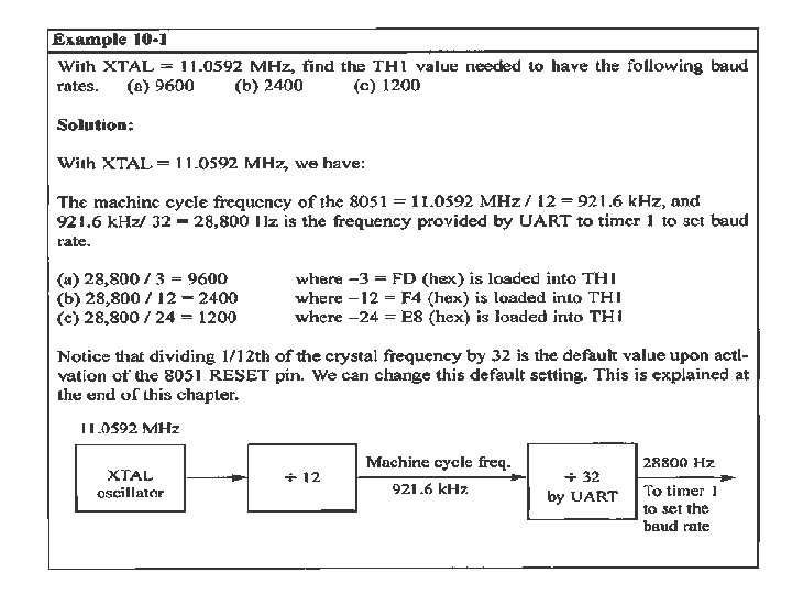
Baud Rate for SMOD=0 Baud Rate for SMOD=1 (Doubling the Baud Rate) TH 1 (decimal) TH 1 (Hex) 9600 19200 -3 FD 4800 9600 -6 FA 2400 4800 -12 F 4 1200 2400 -24 E 8
Programming (Transfer) 1. MOV TMOD, #20 H ; Timer 1, mode 2 2. TH 1 is loaded to set the baud rate. 3. MOV SCON, #50 H SM 0 0 SM 1 1 SM 2 0 REN TB 8 1 0 RB 8 0 TI 0 RI 0 SCON REN=1: allows Tx. D and Rx. D 4. SETB TR 1 ; Run Timer 1 5. MOV SBUF, #’D’ 6. Loop: JNB TI, Loop ; Monitor TI 7. CLR TI 8. Repeat step 5 for next character. 21
Programming (Receive) 1. MOV TMOD, #20 H ; Timer 1, mode 2 2. TH 1 is loaded to set the baud rate. 3. MOV SCON, #50 H SM 0 0 SM 1 1 SM 2 0 REN TB 8 1 0 RB 8 0 TI 0 REN=1: allows Tx. D and Rx. D 4. SETB TR 1 ; Run Timer 1 5. Loop: JNB RI, Loop ; Monitor RI 6. MOV A, SBUF 7. CLR RI 8. Repeat step 5 for next character. RI 0 SCON