PIN DIAGRAM OF 8086 PIN DIAGRAM OF 8086


 • A 40 pin dual in line package.")
 • It has multiplexed address and data bus")


 • The S 4 and S 3 combinedly indicate which segment register")
 • S 2, S 1, S 0 – Status Lines : These")
 : This output pin indicates that other system bus master will be")
 • QS 1, QS 0 – Queue Status: These lines give information")
 • BHE/S 7 : The bus high enable is active low signal.")
 • R Q /G T 0, R Q /G T 1 –")


 • The EU of 8086 tells the BIU where")
 • while EU is decoding an instruction or executing")

 • Additional registers called segment registers generate memory address when combined")


 • Parity Flag (PF): This flag is used to indicate")
 • Sign Flag (SF): In sign magnitude format the sign")

 2. Interrupt Flag (IF): a. It is an interrupt enable/disable")

- Slides: 28
PIN DIAGRAM OF 8086
PIN DIAGRAM OF 8086 (CONT…. ) • A 40 pin dual in line package. • It is a 16 bit μp*. • 8086 has a 20 bit address bus can access upto 2^20 memory locations ( 1 MB). • It can support upto 64 K (2^16) I/O ports. • The 8086 microprocessor has a total of 14 registers that are accessible to the programmer. • Eight of the registers are known as general purpose registers i. e. they can be used by the programmer for data manipulation.
PIN DIAGRAM OF 8086 (CONT…. ) • It has multiplexed address and data bus AD 0 AD 15 and A 16 – A 19. • It requires single phase clock with 33% duty cycle to provide internal timing. • 8086 is designed to operate in two modes, Minimum and Maximum. • It requires +5 V power supply.
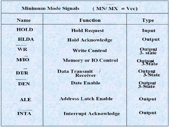
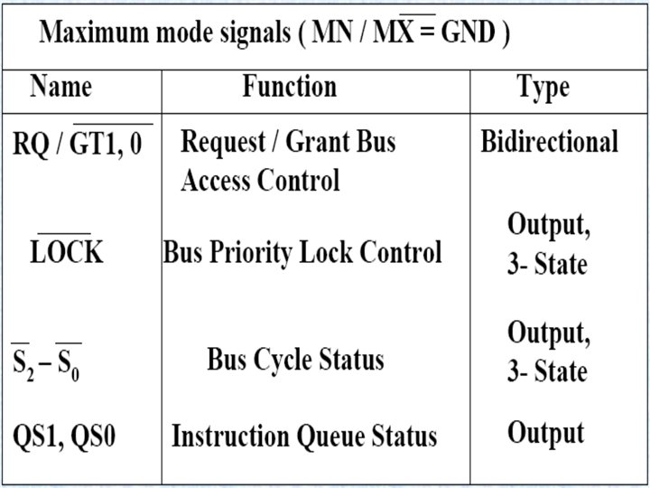
Minimum and Maximum Modes • The minimum mode is selected by applying logic 1 to the MN / MX input pin. This is a single microprocessor configuration. • The maximum mode is selected by applying logic 0 to the MN / MX input pin. This is a multi micro processors configuration.
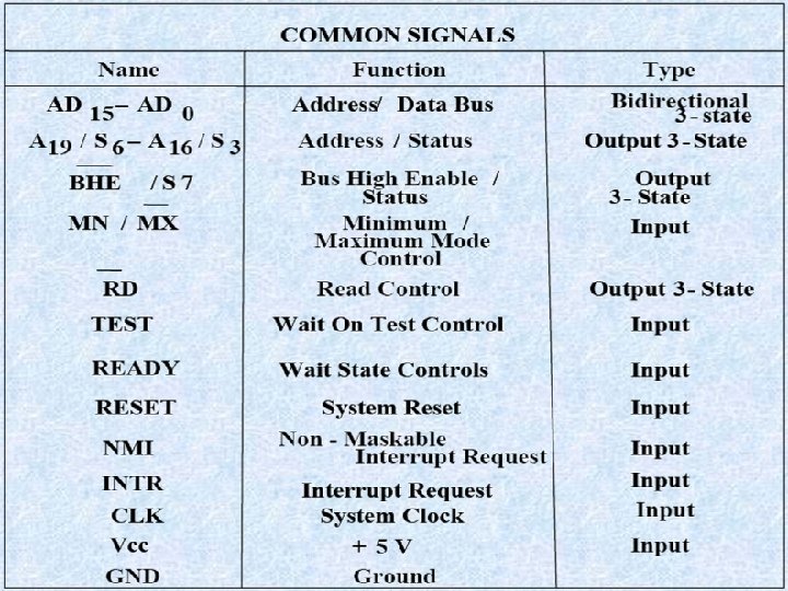
SIGNAL DESCRIPTION • The 8086 signals can be categorised in three groups. • The first are the signal having common functions in minimum as well as maximum mode. • The second are the signals which have special functions for minimum mode • third are the signals having special functions for maximum mode.
SIGNAL DESCRIPTION(cont…) • The S 4 and S 3 combinedly indicate which segment register is presently being used for memory accesses as in below fig. • The status line S 6 is always low. • The address bit are separated from the status bit using latches controlled by the ALE signal.
SIGNAL DESCRIPTION(cont…) • S 2, S 1, S 0 – Status Lines : These are the status lines which reflect the type of operation, being carried out by the processor. These become active during T 4 of the previous cycle and active during T 1 and T 2 of the current bus cycles.
SIGNAL DESCRIPTION(cont…) : This output pin indicates that other system bus master will be prevented from gaining the system bus, while the LOCK signal is low. • This signal indicates the availability of valid data over the address/data lines. It is used to enable the transreceivers ( bidirectional buffers ) to separate the data from the multiplexed address/data signal. It is active from the middle of T 2 until the middle of T 4. This is tristated during ‘hold acknowledge’ cycle. •
SIGNAL DESCRIPTION(cont…) • QS 1, QS 0 – Queue Status: These lines give information about the status of the codeprefetch queue. These are active during the CLK cycle after while the queue operation is performed.
SIGNAL DESCRIPTION(cont…) • BHE/S 7 : The bus high enable is active low signal. It goes low for the data transfer over higher order data bus (D 15 -D 8 ) and is used to derive chip selects of odd address memory bank or peripherals. BHE is low during T 1 for read, write and interrupt acknowledge cycles, whenever a byte is to be transferred on higher byte of data bus. The status information is available during T 2, T 3 and T 4.
SIGNAL DESCRIPTION(cont…) • R Q /G T 0, R Q /G T 1 – Request/Grant : These pins are used by the other local bus master in maximum mode, to force the processor to release the local bus at the end of the processor current bus cycle. • Each of the pin is bidirectional with R Q /G T 0 having higher priority than RQ/GT 1. • RQ/GT pins have internal pull-up resistors and may be left unconnected.
8086 INTERNAL ARCHITECTURE
8086 INTERNAL ARCHITECTURE • 8086 has two blocks BIU and EU. • The purpose of dividing the work between these two units is speeds up the processing. • The BIU sends out addresses, fetches instructions from memory, reads data from memory and ports and writes data to memory and ports. In other words the BIU handles all transfers of data and addresses on buses for the EU. • The instruction bytes are transferred to the instruction queue.
8086 INTERNAL ARCHITECTURE (CONT…. ) • The EU of 8086 tells the BIU where to fetch instructions or data from, decode instructions, and executes instruction. • Bus Interfacr Unit: • It provides a full 16 bit bidirectional data bus and 20 bit address bus. • BIU contains Instruction queue, Segment registers, Instruction pointer, Address adder. • EU contains Control circuitry, Instruction decoder, ALU, Pointer and Index register, Flag register.
8086 INTERNAL ARCHITECTURE (CONT…. ) • while EU is decoding an instruction or executing an instruction which does not require use of the buses, the BIU fetches six instruction bytes and BIU stores these prefetched bytes in a first-in-first-out (FIFO) register set called a queue. • Fetching the next instruction while the current instruction executes is called pipelining.
Segment Registers
Segment Registers (Conti…) • Additional registers called segment registers generate memory address when combined with other in the microprocessor. In 8086 microprocessor, memory is divided into 4 segments. 1. Code Segment (CS): The CS register is used for addressing a memory location in the Code Segment of the memory, where the executable program is stored. 2. Data Segment (DS): The DS contains most data used by program. Data are accessed in the Data Segment by an offset address or the content of other register that holds the offset address. 3. Stack Segment (SS): SS defined the area of memory used for the stack. 4. Extra Segment (ES): ES is additional data segment that is used by some of the string to hold the destination data.
Flag Register of 8086 • A flag is a flip-flop which indicates some condition produced by the execution of an instruction. • A 16 -bit flag register in the EU contains nine active flags. They are divided into two categories: 1. Conditional Flags 2. Control Flags
Conditional Flags • Six of the nine flags are used to indicate some condition produce by an instruction. • Carry Flag (CF): If the addition of two 16 -bit binary numbers produces a carry out of the MSB position then carry flag is set to 1 otherwise it is reset to 0. • Auxiliary Flag (AF): If an operation performed in ALU generates a carry/barrow from lower nibble (i. e. D 0 – D 3) to upper nibble (i. e. D 4 – D 7), the AF flag is set i. e. carry given by D 3 bit to D 4 is AF flag. This is not a general-purpose flag, it is used internally by the processor to perform Binary to BCD conversion.
Conditional Flags (Conti…. ) • Parity Flag (PF): This flag is used to indicate the parity of result. If lower order 8 -bits of the result contains even number of 1’s, the Parity Flag is set and for odd number of 1’s, the Parity Flag is reset. • Zero Flag (ZF): It is set; if the result of arithmetic or logical operation is zero else it is reset.
Conditional Flags (Conti…. ) • Sign Flag (SF): In sign magnitude format the sign of number is indicated by MSB bit. If the result of operation is negative, sign flag is set. • Overflow Flag (OF): It occurs when signed numbers are added or subtracted. An OF indicates that the result has exceeded the capacity of machine.
Control Flags • Three remaining flags in the flags register are used to control certain operations of the processor. Control flags are as follows: 1. Trap Flag (TP): a. It is used for single step control. b. It allows user to execute one instruction of a program at a time for debugging. c. When trap flag is set, program can be run in single step mode.
Control Flags (Conti…. ) 2. Interrupt Flag (IF): a. It is an interrupt enable/disable flag. b. If it is set, the maskable interrupt of 8086 is enabled and if it is reset, the interrupt is disabled. 3. Direction Flag (DF): a. It is used in string operation. b. If it is set, string bytes are accessed from higher memory address to lower memory address. c. When it is reset, the string bytes are accessed from lower memory address to higher memory address.
General Purpose Registers of 8086