Unit3 8085 Microprocessor Prof Swati Sharma swati sharmadarshan







- Slides: 94

Unit-3 8085 Microprocessor Prof. Swati Sharma swati. sharma@darshan. ac. in Unit-3 8085 Microprocessor Darshan Institute of Engineering & Technology Microprocessor & Interfacing - 2150707 Darshan Institute of Engineering & Technology

8085 Architecture Unit-3 8085 Microprocessor Darshan Institute of Engineering & Technology

8085 Architecture § 8085 is pronounced as "eighty-five" microprocessor. § It is an 8 -bit microprocessor designed by Intel in 1977 using NMOS technology. Unit-3 8085 Microprocessor 4 Darshan Institute of Engineering & Technology

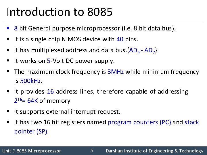
Introduction to 8085 § 8 bit General purpose microprocessor (i. e. 8 bit data bus). § It is a single chip N MOS device with 40 pins. § It has multiplexed address and data bus. (AD 0 - AD 7). § It works on 5 -Volt DC power supply. § The maximum clock frequency is 3 MHz while minimum frequency is 500 k. Hz. § It provides 16 address lines, therefore capable of addressing 216= 64 K of memory. § It supports external interrupt request. § It has two 16 bit registers named program counters (PC) and stack pointer (SP). Unit-3 8085 Microprocessor 5 Darshan Institute of Engineering & Technology

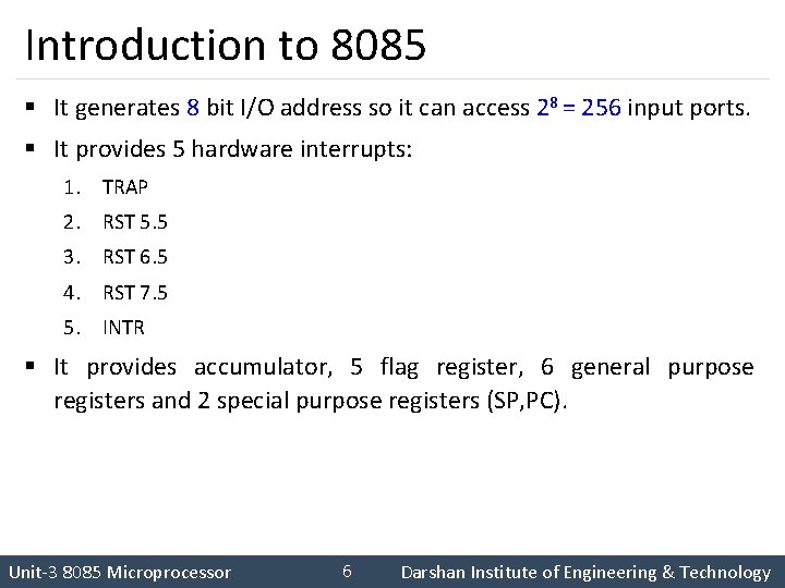
Introduction to 8085 § It generates 8 bit I/O address so it can access 28 = 256 input ports. § It provides 5 hardware interrupts: 1. TRAP 2. RST 5. 5 3. RST 6. 5 4. RST 7. 5 5. INTR § It provides accumulator, 5 flag register, 6 general purpose registers and 2 special purpose registers (SP, PC). Unit-3 8085 Microprocessor 6 Darshan Institute of Engineering & Technology

8085 Programming Model Unit-3 8085 Microprocessor Darshan Institute of Engineering & Technology

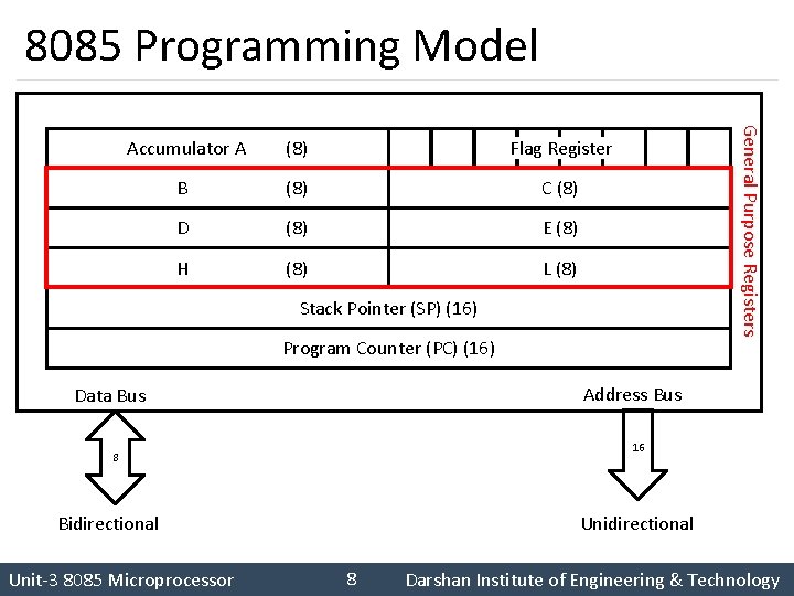
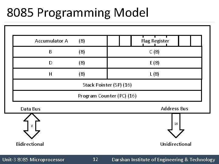
8085 Programming Model (8) Flag Register B (8) C (8) D (8) E (8) H (8) L (8) General Purpose Registers Accumulator A Stack Pointer (SP) (16) Program Counter (PC) (16) Data Bus 8 Bidirectional Address Bus 16 Unidirectional Unit-3 8085 Microprocessor 8 Darshan Institute of Engineering & Technology

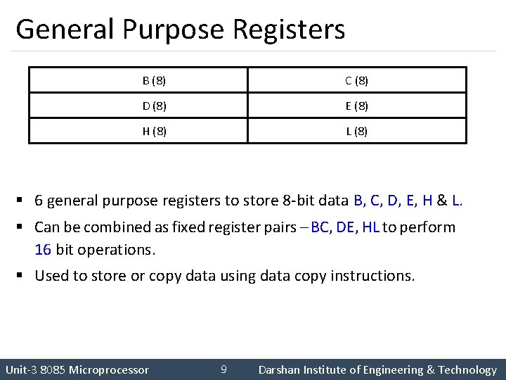
General Purpose Registers B (8) C (8) D (8) E (8) H (8) L (8) § 6 general purpose registers to store 8 -bit data B, C, D, E, H & L. § Can be combined as fixed register pairs – BC, DE, HL to perform 16 bit operations. § Used to store or copy data using data copy instructions. Unit-3 8085 Microprocessor 9 Darshan Institute of Engineering & Technology

8085 Programming Model Accumulator A (8) Flag Register B (8) C (8) D (8) E (8) H (8) L (8) Stack Pointer (SP) (16) Program Counter (PC) (16) Data Bus 8 Bidirectional Address Bus 16 Unidirectional 10 Darshan Institute of Engineering & Technology Unit-3 8085 Microprocessor

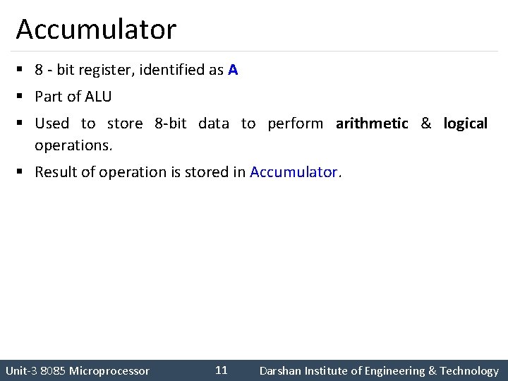
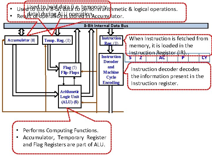
Accumulator § 8 - bit register, identified as A § Part of ALU § Used to store 8 -bit data to perform arithmetic & logical operations. § Result of operation is stored in Accumulator. 11 Darshan Institute of Engineering & Technology Unit-3 8085 Microprocessor

8085 Programming Model Accumulator A (8) Flag Register B (8) C (8) D (8) E (8) H (8) L (8) Stack Pointer (SP) (16) Program Counter (PC) (16) Data Bus 8 Bidirectional Address Bus 16 Unidirectional 12 Darshan Institute of Engineering & Technology Unit-3 8085 Microprocessor

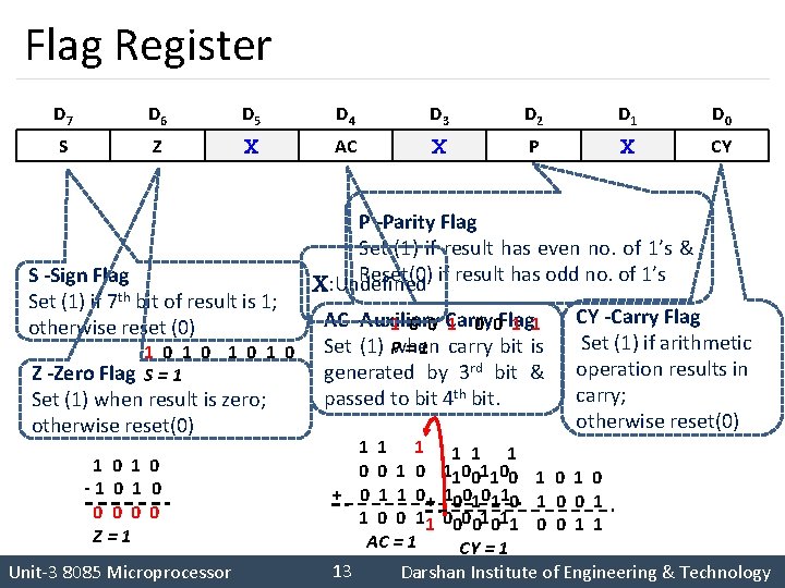
Flag Register D 7 D 6 D 5 D 4 D 3 D 2 D 1 D 0 S Z AC P CY S -Sign Flag Set (1) if 7 th bit of result is 1; otherwise reset (0) 1 0 1 0 Z -Zero Flag S = 1 Set (1) when result is zero; otherwise reset(0) P -Parity Flag Set (1) if result has even no. of 1’s & Reset(0) if result has odd no. of 1’s : Undefined AC -Auxiliary 1 0 0 Carry 1 0 0 Flag 1 1 Set (1) Pwhen = 1 carry bit is generated by 3 rd bit & passed to bit 4 th bit. 1 1 1 0 0 1 0 + 0 1 1 0+ 1 0 0 11 AC = 1 CY -Carry Flag Set (1) if arithmetic operation results in carry; otherwise reset(0) 1 11001100 1 0 10010110 1 00001011 0 0 1 1 CY = 1 13 Darshan Institute of Engineering & Technology Unit-3 8085 Microprocessor 1 0 -1 0 0 0 Z=1

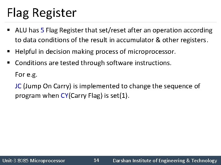
Flag Register § ALU has 5 Flag Register that set/reset after an operation according to data conditions of the result in accumulator & other registers. § Helpful in decision making process of microprocessor. § Conditions are tested through software instructions. For e. g. JC (Jump On Carry) is implemented to change the sequence of program when CY(Carry Flag) is set(1). 14 Darshan Institute of Engineering & Technology Unit-3 8085 Microprocessor

8085 Programming Model Accumulator A (8) Flag Register B (8) C (8) D (8) E (8) H (8) L (8) Stack Pointer (SP) (16) Program Counter (PC) (16) Data Bus 8 Bidirectional Address Bus 16 Unidirectional 15 Darshan Institute of Engineering & Technology Unit-3 8085 Microprocessor

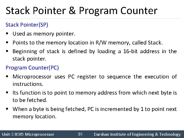
Stack Pointer & Program Counter Stack Pointer(SP) § Used as memory pointer. § Points to the memory location in R/W memory, called Stack. § Beginning of stack is defined by loading a 16 -bit address in the stack pointer. Program Counter(PC) § Microprocessor uses PC register to sequence the execution of instructions. § Its function is to point to memory address from which next byte is to be fetched. § When a byte is being fetched, PC is incremented by 1 to point next memory location. 16 Darshan Institute of Engineering & Technology Unit-3 8085 Microprocessor

Bus Organization of 8085 Unit-3 8085 Microprocessor Darshan Institute of Engineering & Technology

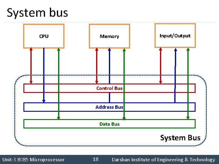
System bus CPU Memory Input/Output Control Bus Address Bus Data Bus System Bus 18 Darshan Institute of Engineering & Technology Unit-3 8085 Microprocessor

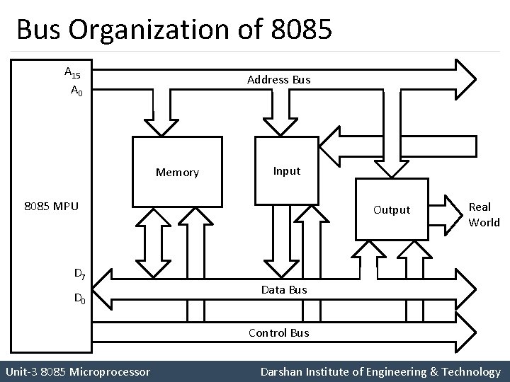
Bus Organization of 8085 A 15 A 0 Address Bus Memory Input 8085 MPU D 7 D 0 Output Real World Data Bus Control Bus Unit-3 8085 Microprocessor Darshan Institute of Engineering & Technology

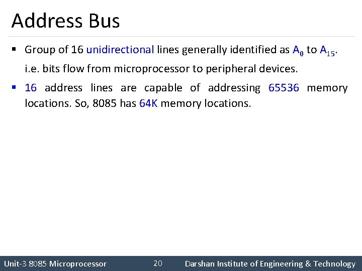
Address Bus § Group of 16 unidirectional lines generally identified as A 0 to A 15. i. e. bits flow from microprocessor to peripheral devices. § 16 address lines are capable of addressing 65536 memory locations. So, 8085 has 64 K memory locations. 20 Darshan Institute of Engineering & Technology Unit-3 8085 Microprocessor

Bus Organization of 8085 A 15 A 0 Address Bus Memory Input 8085 MPU D 7 D 0 Output Real World Data Bus Control Bus Unit-3 8085 Microprocessor Darshan Institute of Engineering & Technology

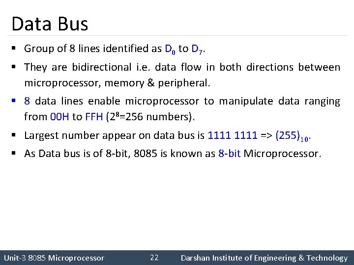
Data Bus § Group of 8 lines identified as D 0 to D 7. § They are bidirectional i. e. data flow in both directions between microprocessor, memory & peripheral. § 8 data lines enable microprocessor to manipulate data ranging from 00 H to FFH (28=256 numbers). § Largest number appear on data bus is 1111 => (255)10. § As Data bus is of 8 -bit, 8085 is known as 8 -bit Microprocessor. 22 Darshan Institute of Engineering & Technology Unit-3 8085 Microprocessor

Bus Organization of 8085 A 15 A 0 Address Bus Memory Input 8085 MPU D 7 D 0 Output Real World Data Bus Control Bus Unit-3 8085 Microprocessor Darshan Institute of Engineering & Technology

Control Bus § It comprises of various single lines that carry synchronization, timing & control signals. § These signals are used to identify a device type with which MPU intends to communicate. § Some control signals are Read, Write and Opcode fetch etc. 24 Darshan Institute of Engineering & Technology Unit-3 8085 Microprocessor

8085 pin diagram Unit-3 8085 Microprocessor Darshan Institute of Engineering & Technology

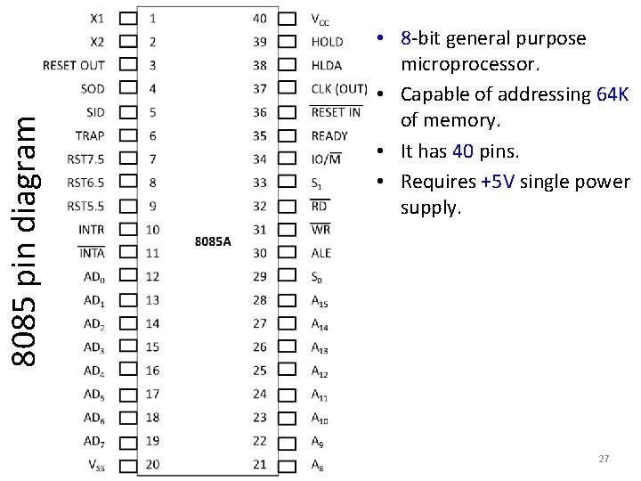
8085 pin diagram • 8 -bit general purpose microprocessor. • Capable of addressing 64 K of memory. • It has 40 pins. • Requires +5 V single power supply. 27

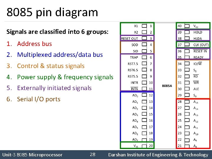
8085 pin diagram Signals are classified into 6 groups: 1. Address bus 2. Multiplexed address/data bus 3. Control & status signals 4. Power supply & frequency signals 5. Externally initiated signals 6. Serial I/O ports 28 Darshan Institute of Engineering & Technology Unit-3 8085 Microprocessor

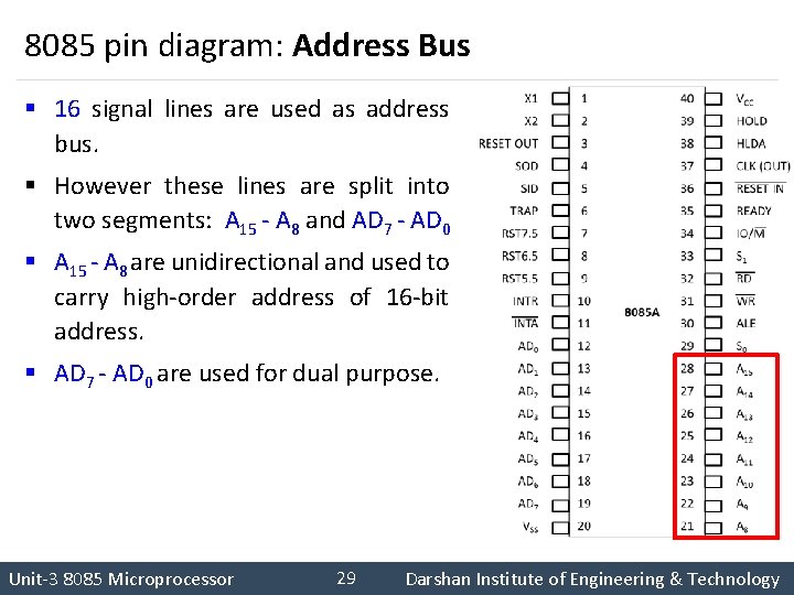
8085 pin diagram: Address Bus § 16 signal lines are used as address bus. § However these lines are split into two segments: A 15 - A 8 and AD 7 - AD 0 § A 15 - A 8 are unidirectional and used to carry high-order address of 16 -bit address. § AD 7 - AD 0 are used for dual purpose. 29 Darshan Institute of Engineering & Technology Unit-3 8085 Microprocessor

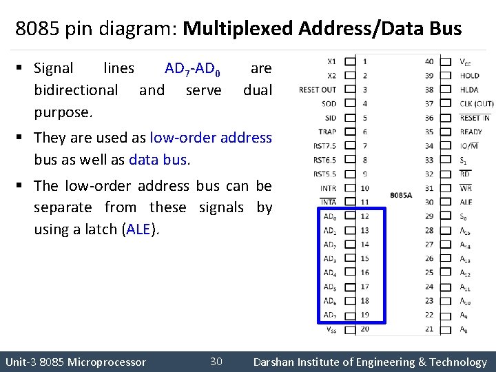
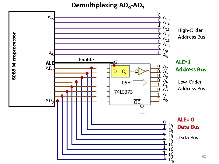
8085 pin diagram: Multiplexed Address/Data Bus § Signal lines AD 7 -AD 0 bidirectional and serve purpose. are dual § They are used as low-order address bus as well as data bus. § The low-order address bus can be separate from these signals by using a latch (ALE). 30 Darshan Institute of Engineering & Technology Unit-3 8085 Microprocessor

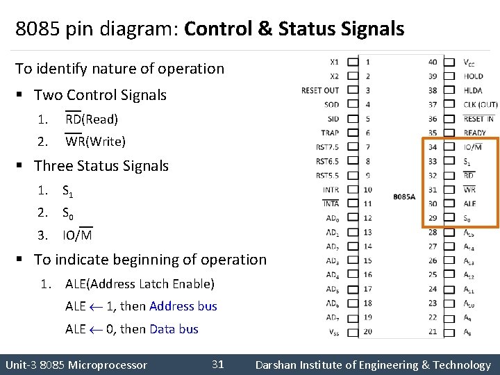
8085 pin diagram: Control & Status Signals To identify nature of operation § Two Control Signals 1. RD(Read) 2. WR(Write) § Three Status Signals 1. S 1 2. S 0 3. IO/M § To indicate beginning of operation 1. ALE(Address Latch Enable) ALE 1, then Address bus ALE 0, then Data bus 31 Darshan Institute of Engineering & Technology Unit-3 8085 Microprocessor

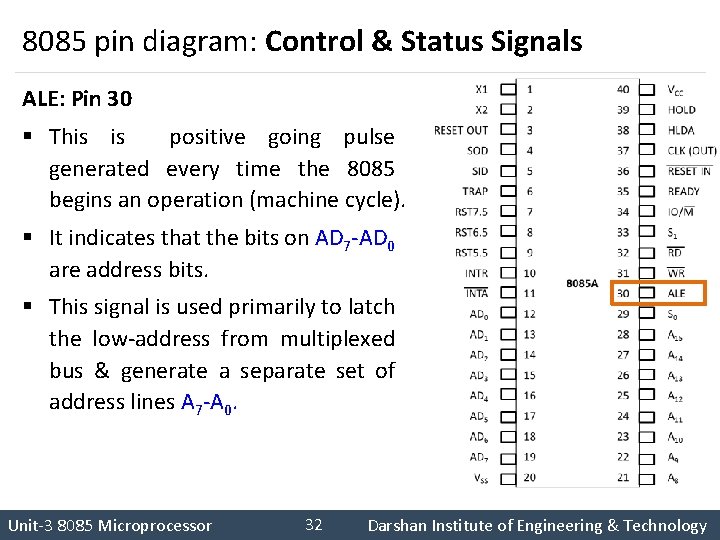
8085 pin diagram: Control & Status Signals ALE: Pin 30 § This is positive going pulse generated every time the 8085 begins an operation (machine cycle). § It indicates that the bits on AD 7 -AD 0 are address bits. § This signal is used primarily to latch the low-address from multiplexed bus & generate a separate set of address lines A 7 -A 0. 32 Darshan Institute of Engineering & Technology Unit-3 8085 Microprocessor

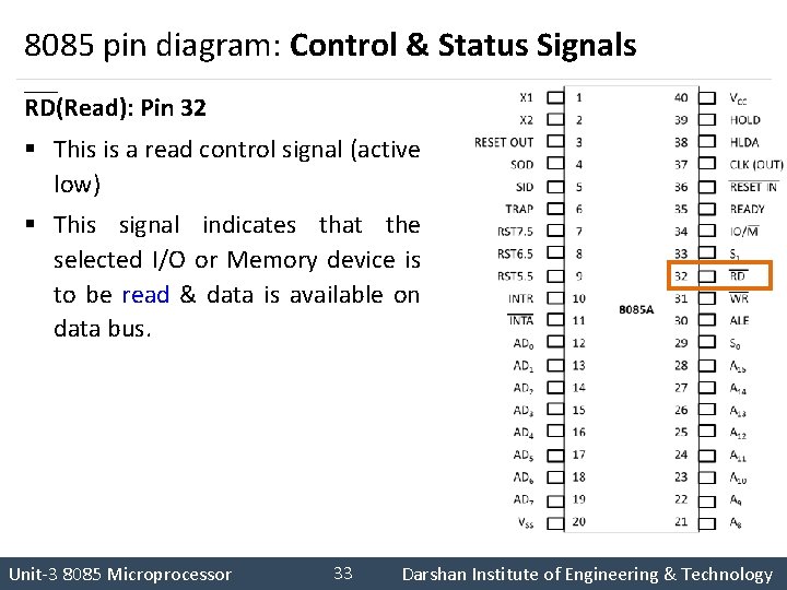
8085 pin diagram: Control & Status Signals RD(Read): Pin 32 § This is a read control signal (active low) § This signal indicates that the selected I/O or Memory device is to be read & data is available on data bus. 33 Darshan Institute of Engineering & Technology Unit-3 8085 Microprocessor

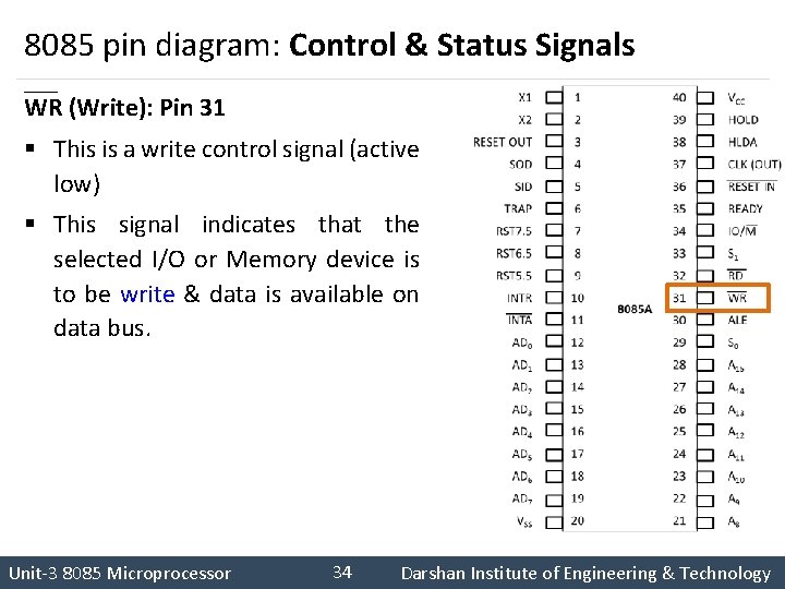
8085 pin diagram: Control & Status Signals WR (Write): Pin 31 § This is a write control signal (active low) § This signal indicates that the selected I/O or Memory device is to be write & data is available on data bus. 34 Darshan Institute of Engineering & Technology Unit-3 8085 Microprocessor

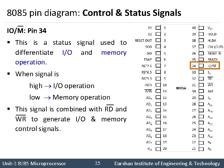
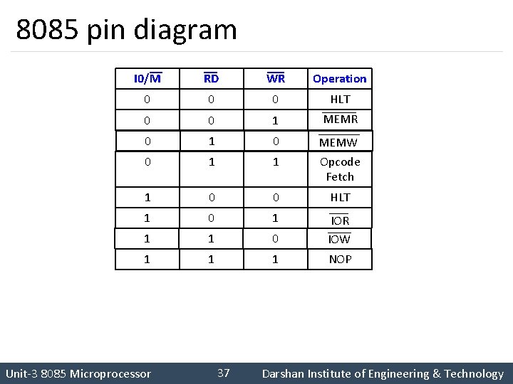
8085 pin diagram: Control & Status Signals IO/M: Pin 34 § This is a status signal used to differentiate I/O and memory operation. § When signal is high I/O operation low Memory operation § This signal is combined with RD and WR to generate I/O & memory control signals. 35 Darshan Institute of Engineering & Technology Unit-3 8085 Microprocessor

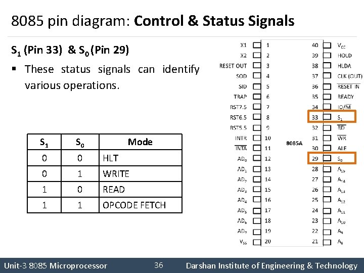
8085 pin diagram: Control & Status Signals S 1 (Pin 33) & S 0 (Pin 29) § These status signals can identify various operations. S 1 S 0 Mode 0 0 HLT 0 1 WRITE 1 0 READ 1 1 OPCODE FETCH 36 Darshan Institute of Engineering & Technology Unit-3 8085 Microprocessor

8085 pin diagram I 0/M RD WR Operation 0 0 0 HLT 0 0 1 MEMR 0 1 0 0 1 1 MEMW Opcode Fetch 1 0 0 HLT 1 0 1 1 1 0 IOR IOW 1 1 1 NOP 37 Darshan Institute of Engineering & Technology Unit-3 8085 Microprocessor

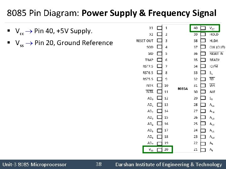
8085 Pin Diagram: Power Supply & Frequency Signal § Vcc Pin 40, +5 V Supply. § Vss Pin 20, Ground Reference 38 Darshan Institute of Engineering & Technology Unit-3 8085 Microprocessor

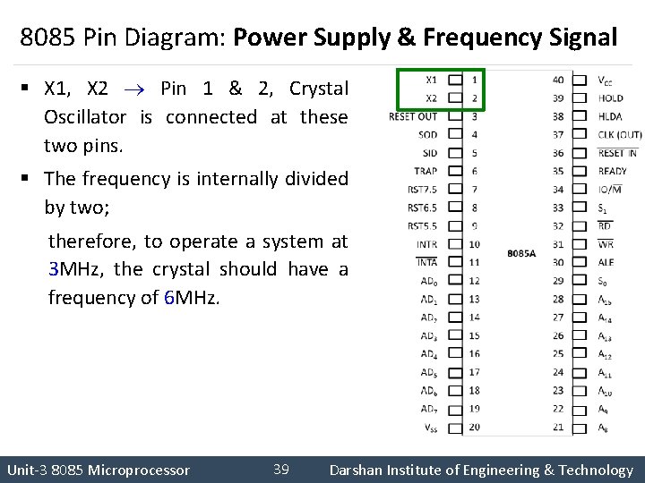
8085 Pin Diagram: Power Supply & Frequency Signal § X 1, X 2 Pin 1 & 2, Crystal Oscillator is connected at these two pins. § The frequency is internally divided by two; therefore, to operate a system at 3 MHz, the crystal should have a frequency of 6 MHz. 39 Darshan Institute of Engineering & Technology Unit-3 8085 Microprocessor

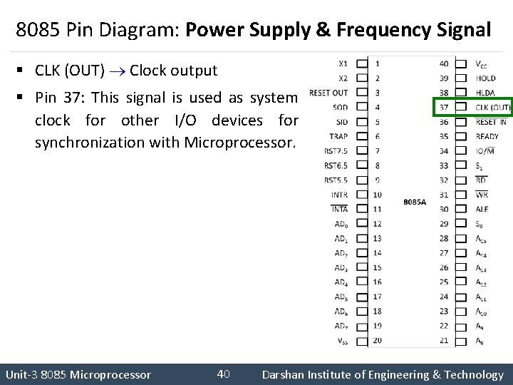
8085 Pin Diagram: Power Supply & Frequency Signal § CLK (OUT) Clock output § Pin 37: This signal is used as system clock for other I/O devices for synchronization with Microprocessor. 40 Darshan Institute of Engineering & Technology Unit-3 8085 Microprocessor

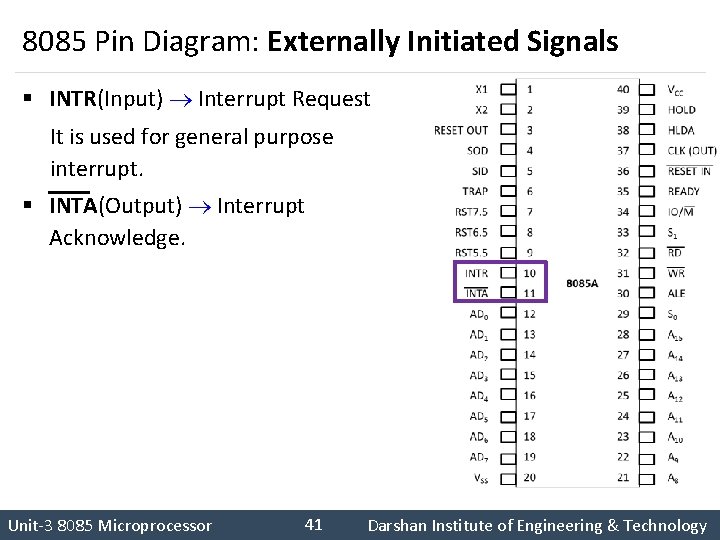
8085 Pin Diagram: Externally Initiated Signals § INTR(Input) Interrupt Request It is used for general purpose interrupt. § INTA(Output) Interrupt Acknowledge. 41 Darshan Institute of Engineering & Technology Unit-3 8085 Microprocessor

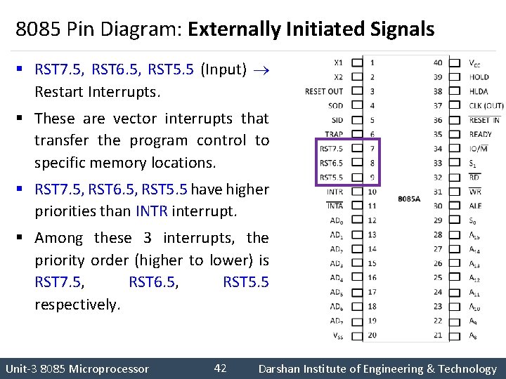
8085 Pin Diagram: Externally Initiated Signals § RST 7. 5, RST 6. 5, RST 5. 5 (Input) Restart Interrupts. § These are vector interrupts that transfer the program control to specific memory locations. § RST 7. 5, RST 6. 5, RST 5. 5 have higher priorities than INTR interrupt. § Among these 3 interrupts, the priority order (higher to lower) is RST 7. 5, RST 6. 5, RST 5. 5 respectively. 42 Darshan Institute of Engineering & Technology Unit-3 8085 Microprocessor

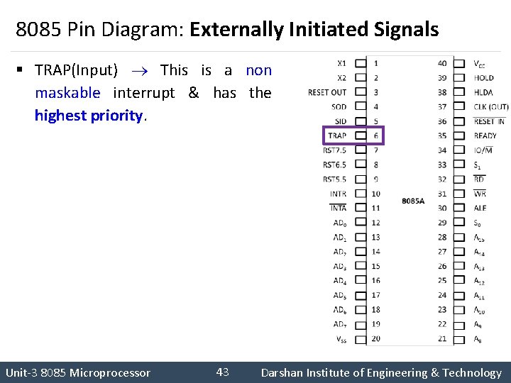
8085 Pin Diagram: Externally Initiated Signals § TRAP(Input) This is a non maskable interrupt & has the highest priority. 43 Darshan Institute of Engineering & Technology Unit-3 8085 Microprocessor

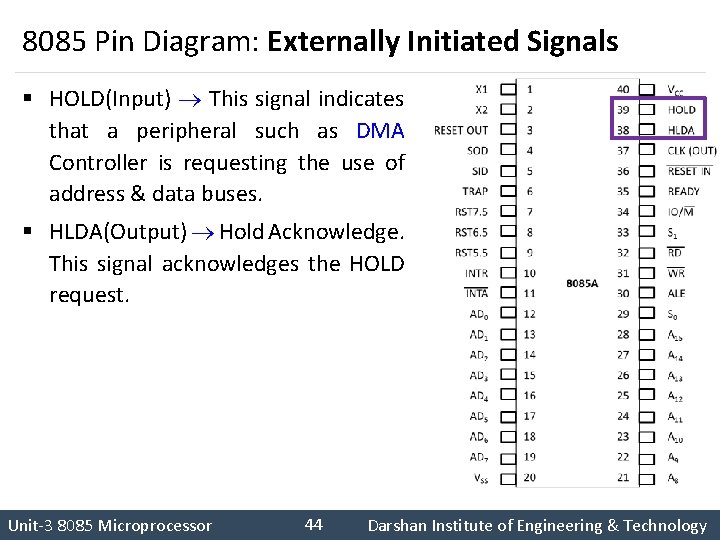
8085 Pin Diagram: Externally Initiated Signals § HOLD(Input) This signal indicates that a peripheral such as DMA Controller is requesting the use of address & data buses. § HLDA(Output) Hold Acknowledge. This signal acknowledges the HOLD request. 44 Darshan Institute of Engineering & Technology Unit-3 8085 Microprocessor

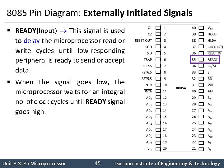
8085 Pin Diagram: Externally Initiated Signals § READY(Input) This signal is used to delay the microprocessor read or write cycles until low-responding peripheral is ready to send or accept data. § When the signal goes low, the microprocessor waits for an integral no. of clock cycles until READY signal goes high. 45 Darshan Institute of Engineering & Technology Unit-3 8085 Microprocessor

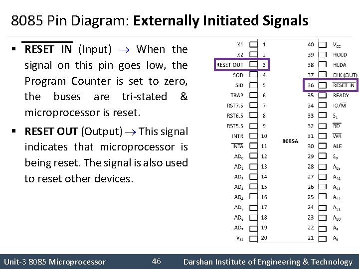
8085 Pin Diagram: Externally Initiated Signals § RESET IN (Input) When the signal on this pin goes low, the Program Counter is set to zero, the buses are tri-stated & microprocessor is reset. § RESET OUT (Output) This signal indicates that microprocessor is being reset. The signal is also used to reset other devices. 46 Darshan Institute of Engineering & Technology Unit-3 8085 Microprocessor

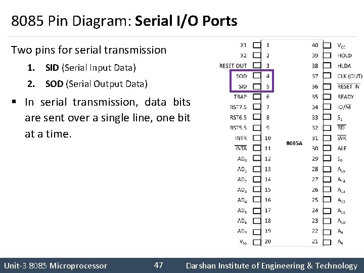
8085 Pin Diagram: Serial I/O Ports Two pins for serial transmission 1. SID (Serial Input Data) 2. SOD (Serial Output Data) § In serial transmission, data bits are sent over a single line, one bit at a time. 47 Darshan Institute of Engineering & Technology Unit-3 8085 Microprocessor

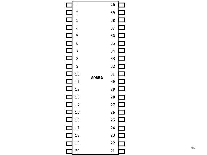
X 1 1 40 VCC X 2 2 39 HOLD RESET OUT 3 38 HLDA SOD 4 37 CLK (OUT) SID 5 36 RESET IN TRAP 6 35 READY RST 7. 5 7 34 IO/M RST 6. 5 8 33 S 1 RST 5. 5 9 32 RD INTR 10 31 WR INTA 11 30 ALE AD 0 12 29 S 0 AD 1 13 28 A 15 AD 2 14 27 A 14 AD 3 15 26 A 13 AD 4 16 25 A 12 AD 5 17 24 A 11 AD 6 18 23 A 10 AD 7 19 22 A 9 VSS 20 21 A 8 8085 A 48

8085 Architecture/Block Diagram Unit-3 8085 Microprocessor Darshan Institute of Engineering & Technology

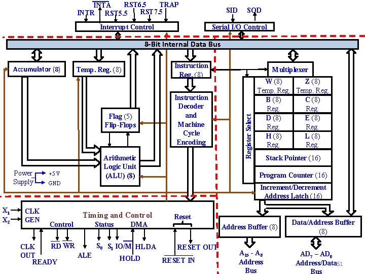
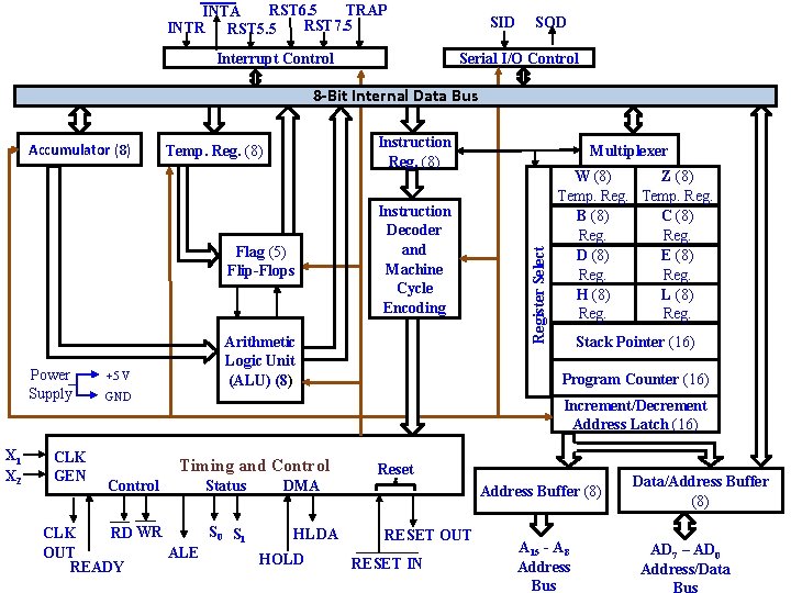
TRAP RST 6. 5 INTA RST 7. 5 INTR RST 5. 5 SID SOD Serial I/O Control Interrupt Control 8 -Bit Internal Data Bus Instruction Reg. (8) Temp. Reg. (8) Flag (5) Flip-Flops Power Supply X 1 X 2 CLK GEN +5 V Instruction Decoder and Machine Cycle Encoding Arithmetic Logic Unit (ALU) (8) W (8) Z (8) Temp. Reg. B (8) C (8) Reg. D (8) E (8) Reg. H (8) L (8) Reg. Stack Pointer (16) Program Counter (16) GND Increment/Decrement Address Latch (16) Timing and Control Multiplexer Register Select Accumulator (8) Status DMA Reset S 0 S 1 IO/M HLDA RD WR CLK RESET OUT ALE OUT HOLD RESET IN READY Address Buffer (8) A 15 - A 8 Address Bus Data/Address Buffer (8) AD 7 – AD 0 Address/Data 51

TRAP RST 6. 5 INTA SID SOD RST 7. 5 Used to hold data (i. e. temporary INTR RST 5. 5 Used to store 8 -bit data to perform arithmetic & logical operations. • data) during ALU operation. Serial I/O Control Interrupt Control • Result of operation is stored in Accumulator. 8 -Bit Internal Data Bus Temp. Reg. (8) Flag (5) Flip-Flops Instruction Reg. (8) Instruction Decoder and Machine Cycle Encoding Arithmetic Logic Unit (ALU) (8) When Instruction is fetched from Multiplexer memory, it is loaded in the W (8) Z (8) Temp. Reg. Instruction Registor (IR). S Z AC P CY B (8) C (8) Reg. D (8) E (8) Instruction decoder decodes Reg. the information present in the H (8) L (8) Instruction register. Register Select Accumulator (8) Stack Pointer (16) Program Counter (16) Increment/Decrement Address Latch (16) X 1 CLK GEN Timing and Control Reset Control Status DMA • Performs Computing Functions. • Accumulator, Temporary Register S 0 S 1 RD WR CLK HLDA RESET OUT and Flag Registers are part of ALU. ALE OUT READY HOLD RESET IN Address Buffer (8) A 15 - A 8 Address Bus Data/Address Buffer (8) AD 7 – AD 0 Address/Data 52

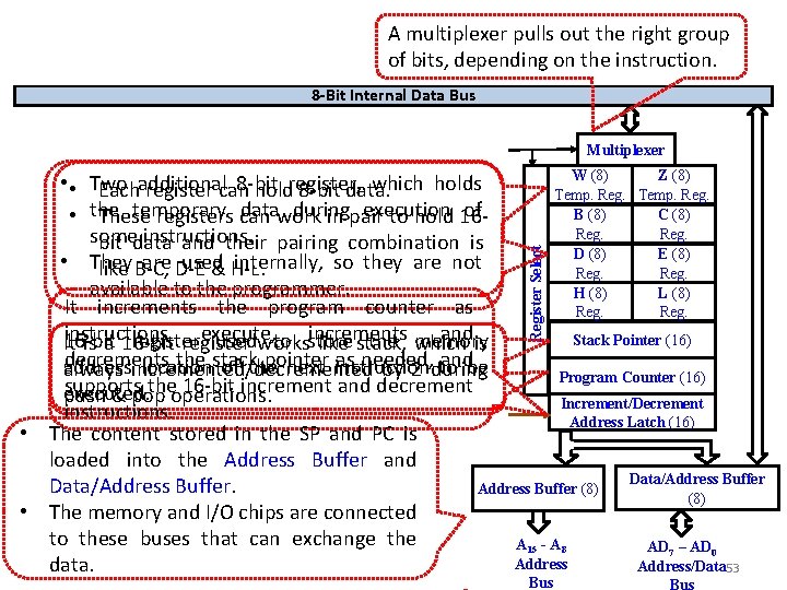
TRAP RST 6. 5 INTA SID SOD RST 7. 5 INTR RST 5. 5 A multiplexer pulls out the right group Interrupt Control Serial I/O Control of bits, depending on the instruction. 8 -Bit Internal Data Bus Accumulator (8) Temp. Reg. (8) Instruction Reg. (8) Multiplexer W (8) Z (8) Two additional 8 -bit register, which holds Each register can hold 8 -bit data. Temp. Reg. Instruction of the temporary data during execution B (8) C (8) These registers can work in pair to hold 16 Decoder Reg. some instructions. bit data and their pairing combination is and Flag (5) D (8) E (8) • They are used internally, so they are not Machine Flip-Flops like B-C, D-E & H-L. Reg. Cycle available to the programmer. H (8) L (8) Encoding as It increments the program counter Reg. instructions execute, increments and is Arithmetic Stack Pointer (16) 16 -bit register used to store the memory It is a 16 -bit register works like stack, which Logic Unit decrements the stack pointer as needed, and address location of the next instruction to be always incremented/decremented by 2 during Program Counter (16) (ALU) (8) supports the 16 -bit increment and decrement executed. push & pop operations. Increment/Decrement instructions. Address Latch (16) • The content stored in the SP and PC is X 1 CLK loaded into the Address Buffer Reset and Timing and Control GEN Data/Address Buffer Control Status DMA Data/Address Buffer. Address Buffer (8) • The memory and I/O chips are connected S 0 S 1 RD WR CLK HLDA RESET OUT to these buses that can exchange the A 15 - A 8 AD 7 – AD 0 ALE OUT HOLD RESET IN Address READY Address/Data 53 data. Register Select • • • Bus

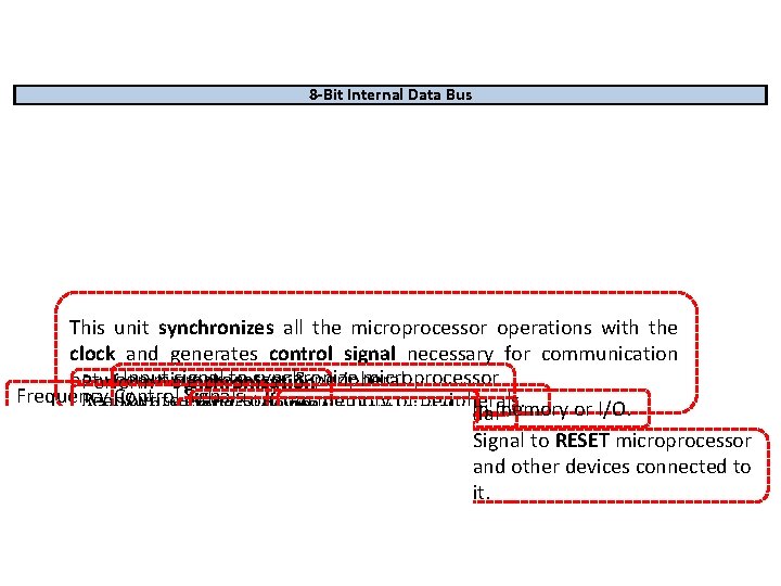
TRAP RST 6. 5 INTA RST 7. 5 INTR RST 5. 5 SID SOD Serial I/O Control Interrupt Control 8 -Bit Internal Data Bus Instruction Reg. (8) Temp. Reg. (8) Flag (5) Flip-Flops Instruction Decoder and Machine Cycle Encoding Multiplexer Register Select Accumulator (8) W (8) Z (8) Temp. Reg. B (8) C (8) Reg. D (8) E (8) Reg. H (8) L (8) Reg. This unit synchronizes all the microprocessor operations with the Arithmetic Stack Pointer (16) clock and generates control signal necessary for communication Logic Unit Program Counter (16) (ALU) (8) Input signal to synchronize microprocessor between microprocessor & peripheral. Perform synchronization Frequency Control Signals Increment/Decrement Read/write either to/from memory or peripherals. with peripheral device. DMA control signal with peripheral device. Shows read/write status to/from memory or I/O. Address Latch Enable control signal Address Latch (16) Signal to RESET microprocessor X 1 CLK Timing and Control Reset and other devices connected to X 2 GEN Data/Address Buffer Control Status DMA Address Buffer (8) it. (8) RD WR CLK S 0 ALE OUT READY S 1 HLDA HOLD RESET OUT RESET IN A 15 - A 8 Address Bus AD 7 – AD 0 Address/Data 54

TRAP RST 6. 5 INTA RST 7. 5 INTR RST 5. 5 SID SOD Serial I/O Control Interrupt Control 8 -Bit Internal Data Bus Instruction Reg. (8) Temp. Reg. (8) Flag (5) Flip-Flops Instruction Decoder and Machine Cycle Encoding Arithmetic Logic Unit (ALU) (8) Multiplexer Register Select Accumulator (8) W (8) Z (8) Temp. Reg. B (8) C (8) Reg. D (8) E (8) Reg. H (8) L (8) Reg. Stack Pointer (16) Program Counter (16) Increment/Decrement Address Latch (16) X 1 X 2 CLK GEN Timing and Control Status RD WR CLK S 0 ALE OUT READY S 1 DMA HLDA HOLD Reset Address Buffer (8) RESET OUT RESET IN A 15 - A 8 Address Bus Data/Address Buffer (8) AD 7 – AD 0 Address/Data 55

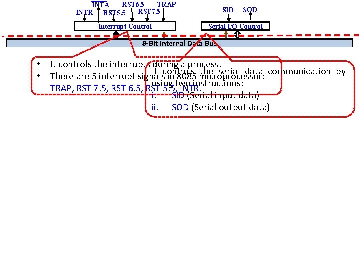
TRAP RST 6. 5 INTA RST 7. 5 INTR RST 5. 5 SID SOD Serial I/O Control Interrupt Control 8 -Bit Internal Data Bus Register Select Instruction • It controls the interrupts during a process. Accumulator (8) Temp. Reg. (8) Multiplexer It controls the serial data communication Reg. (8) • There are 5 interrupt signals in 8085 microprocessor: W (8) Z (8) using two instructions: TRAP, RST 7. 5, RST 6. 5, RST 5. 5, INTR. Temp. Reg. i. Instruction SID (Serial input data) B (8) C (8) Decoder Reg. ii. SOD (Serial output data) and Flag (5) D (8) E (8) Machine Flip-Flops Reg. Cycle H (8) L (8) Encoding Reg. Arithmetic Logic Unit (ALU) (8) by Stack Pointer (16) Program Counter (16) Increment/Decrement Address Latch (16) X 1 X 2 CLK GEN Timing and Control Status RD WR CLK S 0 ALE OUT READY S 1 DMA HLDA HOLD Reset Address Buffer (8) RESET OUT RESET IN A 15 - A 8 Address Bus Data/Address Buffer (8) AD 7 – AD 0 Address/Data 56

TRAP RST 6. 5 INTA RST 7. 5 INTR RST 5. 5 SID SOD Serial I/O Control Interrupt Control 8 -Bit Internal Data Bus Instruction Reg. (8) Temp. Reg. (8) Flag (5) Flip-Flops Power Supply X 1 X 2 CLK GEN +5 V Instruction Decoder and Machine Cycle Encoding Arithmetic Logic Unit (ALU) (8) W (8) Z (8) Temp. Reg. B (8) C (8) Reg. D (8) E (8) Reg. H (8) L (8) Reg. Stack Pointer (16) Program Counter (16) GND Increment/Decrement Address Latch (16) Timing and Control Multiplexer Register Select Accumulator (8) Status DMA Reset S 0 S 1 RD WR CLK HLDA RESET OUT ALE OUT HOLD RESET IN READY Address Buffer (8) A 15 - A 8 Address Bus Data/Address Buffer (8) AD 7 – AD 0 Address/Data

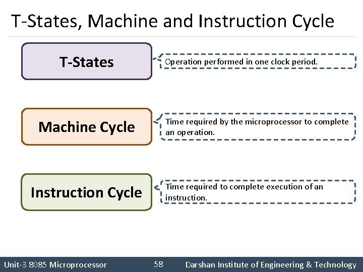
T-States, Machine and Instruction Cycle T-States Machine Cycle Instruction Cycle Operation performed in one clock period. Time required by the microprocessor to complete an operation. Time required to complete execution of an instruction. 58 Darshan Institute of Engineering & Technology Unit-3 8085 Microprocessor

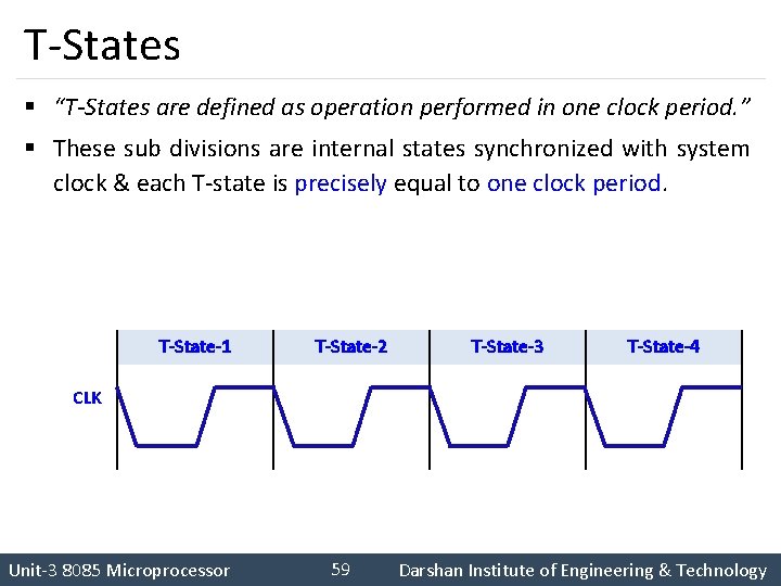
T-States § “T-States are defined as operation performed in one clock period. ” § These sub divisions are internal states synchronized with system clock & each T-state is precisely equal to one clock period. T-State-1 T-State-2 T-State-3 T-State-4 CLK 59 Darshan Institute of Engineering & Technology Unit-3 8085 Microprocessor

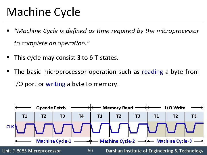
Machine Cycle § “Machine Cycle is defined as time required by the microprocessor to complete an operation. “ § This cycle may consist 3 to 6 T-states. § The basic microprocessor operation such as reading a byte from I/O port or writing a byte to memory. Opcode Fetch T 1 T 2 T 3 Memory Read T 4 T 1 T 2 I/O Write T 3 T 1 T 2 T 3 CLK Machine Cycle-1 Machine Cycle-2 Machine Cycle-3 60 Darshan Institute of Engineering & Technology Unit-3 8085 Microprocessor

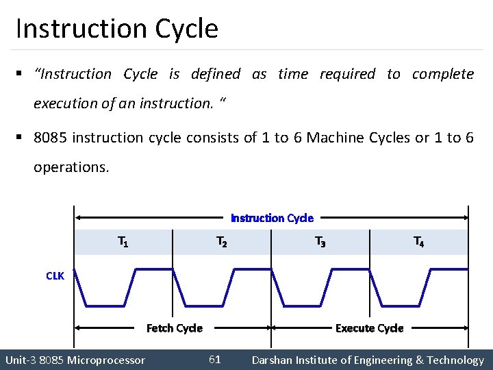
Instruction Cycle § “Instruction Cycle is defined as time required to complete execution of an instruction. “ § 8085 instruction cycle consists of 1 to 6 Machine Cycles or 1 to 6 operations. Instruction Cycle T 1 T 2 T 3 T 4 CLK Fetch Cycle Execute Cycle 61 Darshan Institute of Engineering & Technology Unit-3 8085 Microprocessor

Demultiplexing AD 0 -AD 7 0 0 1 0 0 0 8085 Microprocessor A 15 A 8 ALE AD 7 AD 0 Enable G 0 0 1 0 1 1 A 15 A 14 A 13 A 12 A 11 A 10 A 9 A 8 High-Order Address Bus ALE=1 Address Bus A 7 A 6 A 5 A 4 A 3 A 2 A 1 A 0 0 1 1 1 1 Low-Order Address Bus ALE= 0 D 7 Data Bus D 6 D 5 D 4 Data Bus D 3 D 2 D 1 D 0 62

Memory Interfacing Unit-3 8085 Microprocessor Darshan Institute of Engineering & Technology

Memory Interfacing § When we are executing any instruction, we need microprocessor to access the memory for reading instruction codes and the data stored in the memory. § For this, both the memory and the microprocessor requires some signals to read/write to or from registers. § The interfacing circuit therefore, should be designed in such a way that it matches the memory signal requirements with the signals of the microprocessor. 64 Darshan Institute of Engineering & Technology Unit-3 8085 Microprocessor

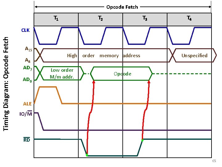
Opcode Fetch T 1 T 2 T 3 T 4 Timing Diagram: Opcode Fetch CLK A 15 A 8 AD 7 AD 0 High order memory address Low order M/m addr. Unspecified Opcode ALE IO/M RD 65

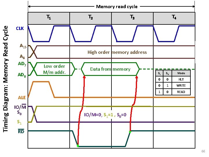
Memory read cycle Timing Diagram: Memory Read Cycle T 1 T 2 T 3 T 4 CLK A 15 A 8 AD 7 AD 0 High order memory address Low order M/m addr. Data from memory S 1 S 0 Mode 0 0 HLT 0 1 WRITE 1 0 READ ALE IO/M S 0 S 1 IO/M=0, S 1=1 , S 0=0 RD 66

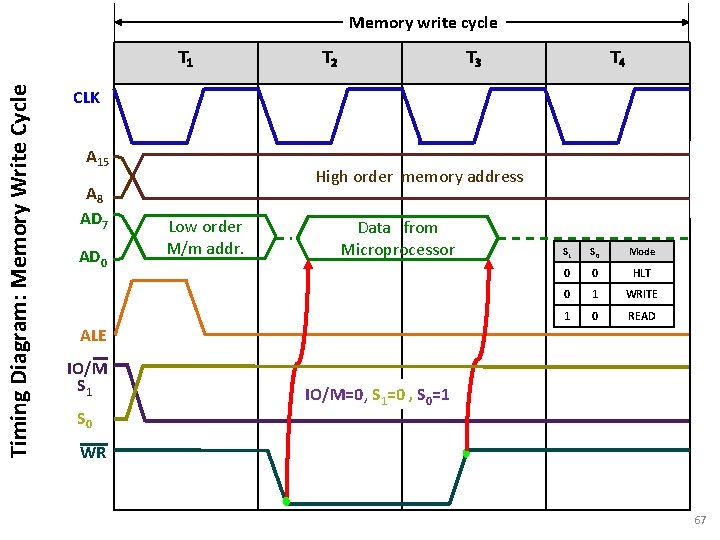
Memory write cycle Timing Diagram: Memory Write Cycle T 1 T 2 T 3 T 4 CLK A 15 A 8 AD 7 AD 0 High order memory address Low order M/m addr. Data from Microprocessor S 1 S 0 Mode 0 0 HLT 0 1 WRITE 1 0 READ ALE IO/M S 1 S 0 IO/M=0, S 1=0 , S 0=1 WR 67

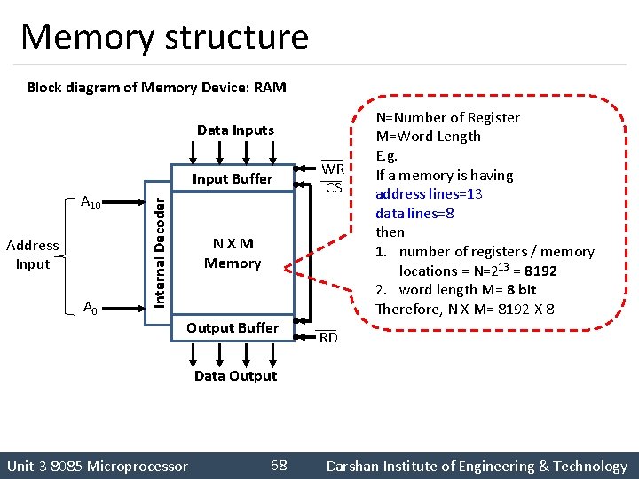
Memory structure Block diagram of Memory Device: RAM Data Inputs A 10 Address Input A 0 Internal Decoder Input Buffer WR CS NXM Memory Output Buffer N=Number of Register M=Word Length E. g. If a memory is having address lines=13 data lines=8 then 1. number of registers / memory locations = N=213 = 8192 2. word length M= 8 bit Therefore, N X M= 8192 X 8 RD Data Output 68 Darshan Institute of Engineering & Technology Unit-3 8085 Microprocessor

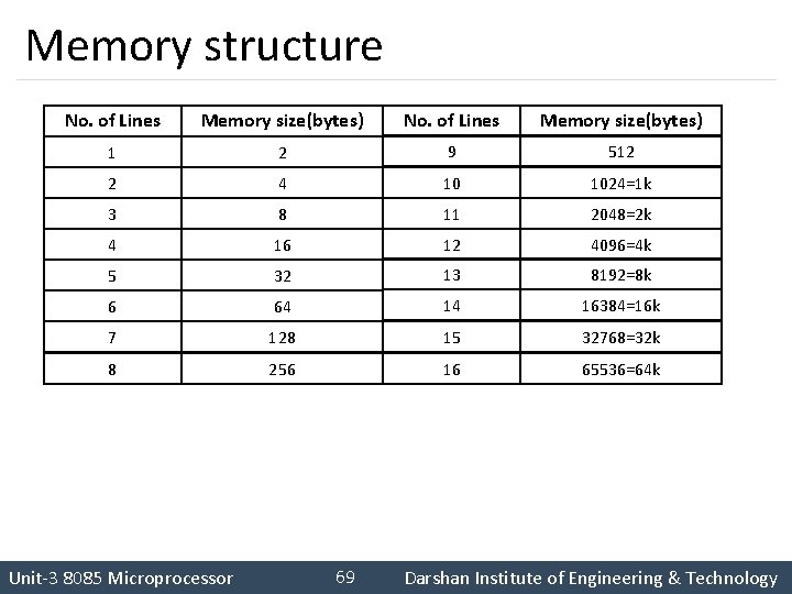
Memory structure No. of Lines Memory size(bytes) 1 2 9 512 2 4 10 1024=1 k 3 8 11 2048=2 k 4 16 12 4096=4 k 5 32 13 8192=8 k 6 64 14 16384=16 k 7 128 15 32768=32 k 8 256 16 65536=64 k 69 Darshan Institute of Engineering & Technology Unit-3 8085 Microprocessor

Memory Interfacing § 8085 can access 64 K of memory, thus address bus is of 16 -bit. § But it is not always necessary to use full 64 K address space. The total memory size depends upon the application. § Generally EPROM is used as a program memory and RAM is used as data memory. § When both are used then total 64 K address will be shared by both. § The capacity of program memory and data memory depends on the application. 70 Darshan Institute of Engineering & Technology Unit-3 8085 Microprocessor

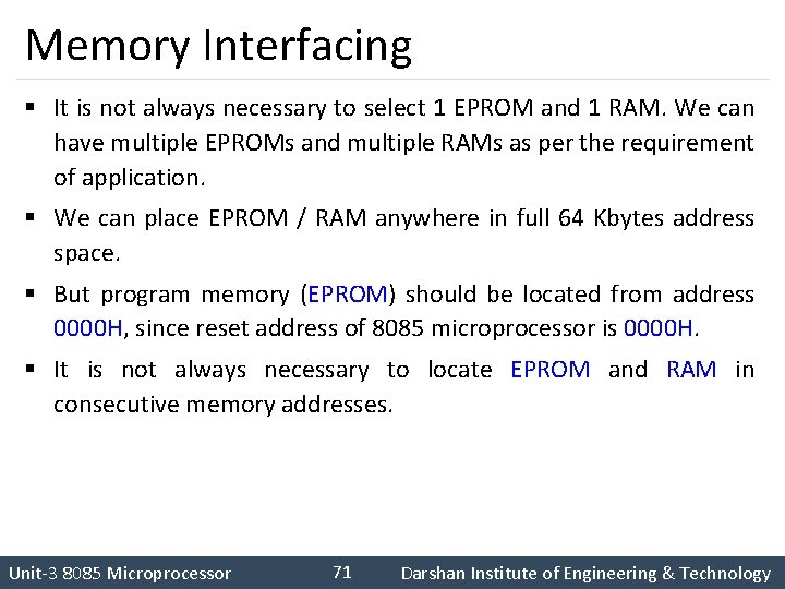
Memory Interfacing § It is not always necessary to select 1 EPROM and 1 RAM. We can have multiple EPROMs and multiple RAMs as per the requirement of application. § We can place EPROM / RAM anywhere in full 64 Kbytes address space. § But program memory (EPROM) should be located from address 0000 H, since reset address of 8085 microprocessor is 0000 H. § It is not always necessary to locate EPROM and RAM in consecutive memory addresses. 71 Darshan Institute of Engineering & Technology Unit-3 8085 Microprocessor

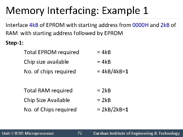
Memory Interfacing: Example 1 Interface 4 k. B of EPROM with starting address from 0000 H and 2 k. B of RAM with starting address followed by EPROM Step-1: Total EPROM required = 4 k. B Chip size available = 4 k. B No. of chips required = 4 k. B/4 k. B=1 Total RAM required = 2 k. B Chip Size Available = 2 k. B No. of Chips required = 2 k. B/2 k. B=1 72 Darshan Institute of Engineering & Technology Unit-3 8085 Microprocessor

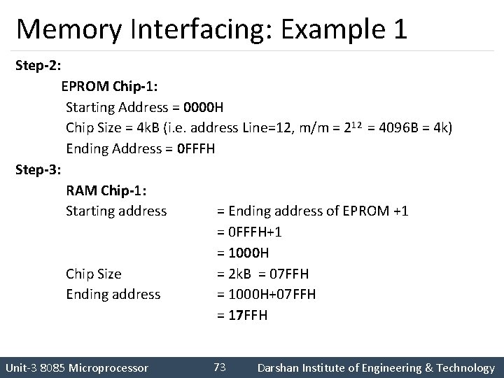
Memory Interfacing: Example 1 Step-2: EPROM Chip-1: Starting Address = 0000 H Chip Size = 4 k. B (i. e. address Line=12, m/m = 212 = 4096 B = 4 k) Ending Address = 0 FFFH Step-3: RAM Chip-1: Starting address = Ending address of EPROM +1 = 0 FFFH+1 = 1000 H Chip Size = 2 k. B = 07 FFH Ending address = 1000 H+07 FFH = 17 FFH 73 Darshan Institute of Engineering & Technology Unit-3 8085 Microprocessor

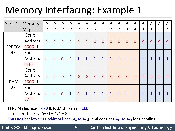
Memory Interfacing: Example 1 Step-4: Memory A A 15 14 13 12 Map Start Address 0 0 EPROM 0000 H End 4 k Address 0 0 0 FFF H Start Address 0 0 0 1 RAM 1000 H End 2 k Address 0 0 0 1 17 FF H A A A 11 10 9 8 7 6 5 4 3 2 1 0 0 0 0 0 0 0 1 1 1 1 1 1 EPROM chip size = 4 k. B & RAM chip size = 2 k. B smaller chip size RAM = 2 k. B = 211 Thus neglect lower 11 address lines (A 0 to A 10), and consider A 11 to A 15 for Decoding. 74 Darshan Institute of Engineering & Technology Unit-3 8085 Microprocessor

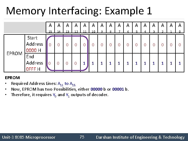
Memory Interfacing: Example 1 Start Address 0000 H EPROM End Address 0 FFF H A A A A 15 14 13 12 11 10 9 8 7 6 5 4 3 2 1 0 0 0 0 0 0 1 1 1 EPROM • Required Address Lines: A 11 to A 15. • Now, EPROM has two Possibilities, either 00000 b or 00001 b. • Therefore, it requires Y 0 and Y 1 outputs of decoder. 75 Darshan Institute of Engineering & Technology Unit-3 8085 Microprocessor

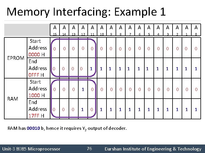
Memory Interfacing: Example 1 Start Address 0000 H EPROM End Address 0 FFF H Start Address 1000 H RAM End Address 17 FF H A A A A 15 14 13 12 11 10 9 8 7 6 5 4 3 2 1 0 0 0 0 0 1 1 1 0 0 0 1 0 0 0 0 1 1 1 0 RAM has 00010 b, hence it requires Y 2 output of decoder. 76 Darshan Institute of Engineering & Technology Unit-3 8085 Microprocessor

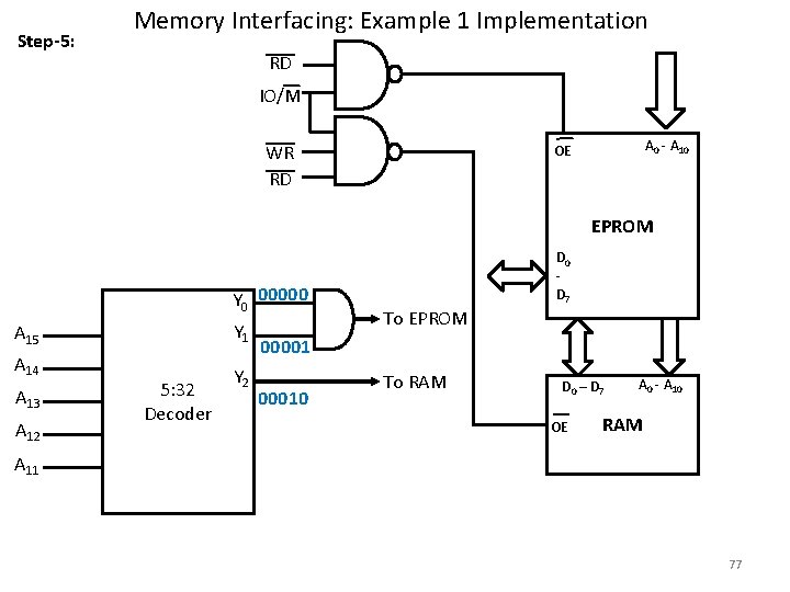
Step-5: Memory Interfacing: Example 1 Implementation RD IO/M WR RD A 0 - A 10 OE EPROM Y 0 00000 Y 1 A 15 A 14 A 13 A 12 5: 32 Decoder Y 2 D 0 D 7 To EPROM 000010 To RAM D 0 – D 7 OE A 0 - A 10 RAM A 11 77

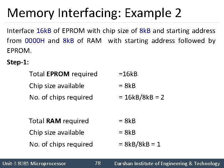
Memory Interfacing: Example 2 Interface 16 k. B of EPROM with chip size of 8 k. B and starting address from 0000 H and 8 k. B of RAM with starting address followed by EPROM. Step-1: Total EPROM required =16 k. B Chip size available = 8 k. B No. of chips required = 16 k. B/8 k. B = 2 Total RAM required = 8 k. B Chip size available = 8 k. B No. of chips required = 8 k. B/8 k. B = 1 78 Darshan Institute of Engineering & Technology Unit-3 8085 Microprocessor

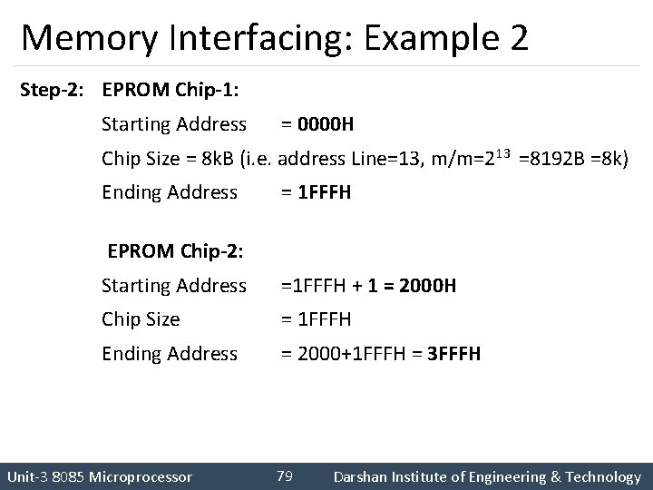
Memory Interfacing: Example 2 Step-2: EPROM Chip-1: Starting Address = 0000 H Chip Size = 8 k. B (i. e. address Line=13, m/m=213 =8192 B =8 k) Ending Address = 1 FFFH EPROM Chip-2: Starting Address =1 FFFH + 1 = 2000 H Chip Size = 1 FFFH Ending Address = 2000+1 FFFH = 3 FFFH 79 Darshan Institute of Engineering & Technology Unit-3 8085 Microprocessor

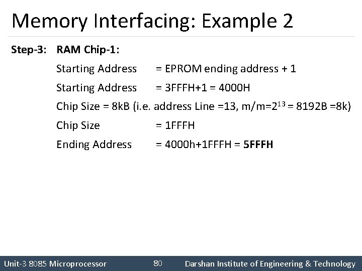
Memory Interfacing: Example 2 Step-3: RAM Chip-1: Starting Address = EPROM ending address + 1 Starting Address = 3 FFFH+1 = 4000 H Chip Size = 8 k. B (i. e. address Line =13, m/m=213 = 8192 B =8 k) Chip Size = 1 FFFH Ending Address = 4000 h+1 FFFH = 5 FFFH 80 Darshan Institute of Engineering & Technology Unit-3 8085 Microprocessor

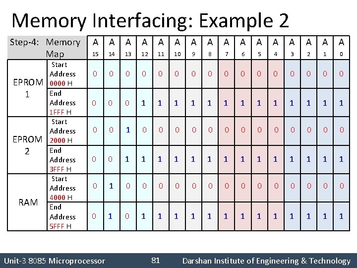
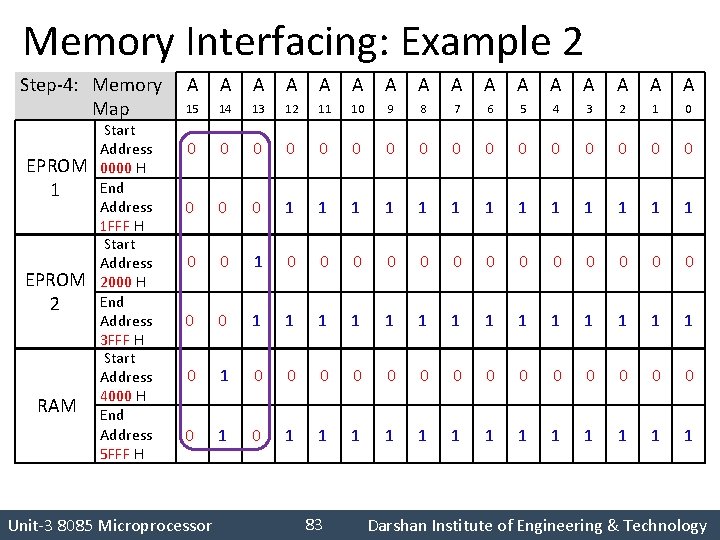
Memory Interfacing: Example 2 Step-4: Memory Map EPROM 1 EPROM 2 RAM Start Address 0000 H End Address 1 FFF H Start Address 2000 H End Address 3 FFF H Start Address 4000 H End Address 5 FFF H A A A A 15 14 13 12 11 10 9 8 7 6 5 4 3 2 1 0 0 0 0 0 1 1 1 1 0 0 0 0 0 1 1 1 1 0 1 0 0 0 0 1 1 1 1 81 Darshan Institute of Engineering & Technology Unit-3 8085 Microprocessor

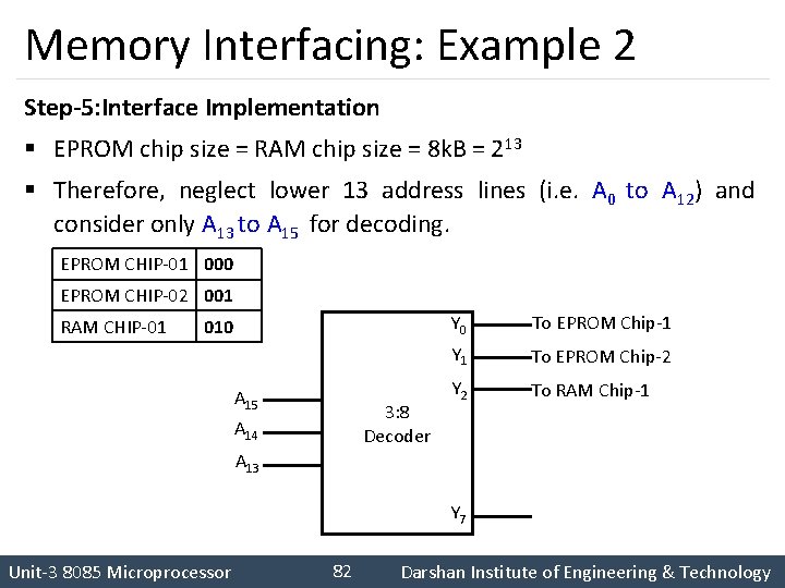
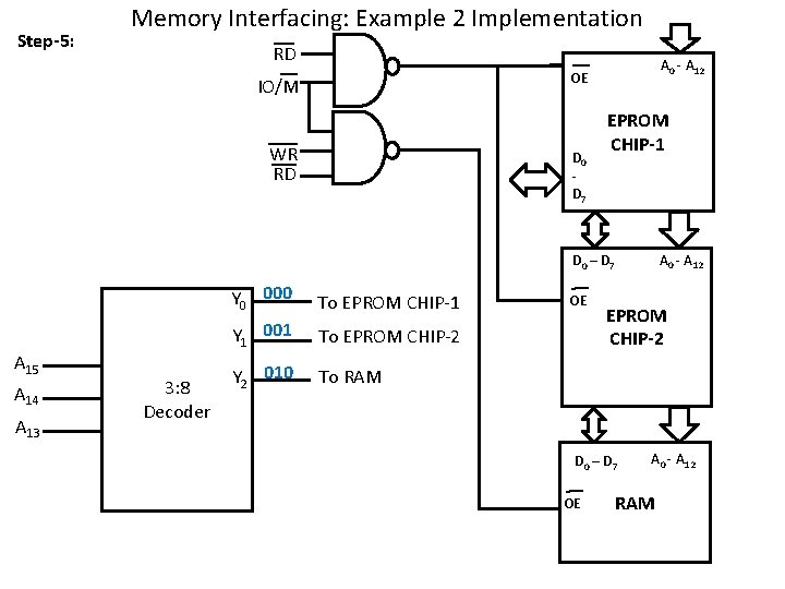
Memory Interfacing: Example 2 Step-5: Interface Implementation § EPROM chip size = RAM chip size = 8 k. B = 213 § Therefore, neglect lower 13 address lines (i. e. A 0 to A 12) and consider only A 13 to A 15 for decoding. EPROM CHIP-01 000 EPROM CHIP-02 001 RAM CHIP-01 010 A 15 A 14 3: 8 Decoder Y 0 To EPROM Chip-1 Y 1 To EPROM Chip-2 Y 2 To RAM Chip-1 A 13 Y 7 82 Darshan Institute of Engineering & Technology Unit-3 8085 Microprocessor

Memory Interfacing: Example 2 Step-4: Memory Map EPROM 1 EPROM 2 RAM Start Address 0000 H End Address 1 FFF H Start Address 2000 H End Address 3 FFF H Start Address 4000 H End Address 5 FFF H A A A A 15 14 13 12 11 10 9 8 7 6 5 4 3 2 1 0 0 0 0 0 1 1 1 1 0 0 0 0 0 1 1 1 1 0 1 0 0 0 0 1 1 1 1 83 Darshan Institute of Engineering & Technology Unit-3 8085 Microprocessor

Step-5: Memory Interfacing: Example 2 Implementation RD A 0 - A 12 OE IO/M WR RD D 0 D 7 EPROM CHIP-1 A 0 - A 12 D 0 – D 7 A 15 A 14 A 13 3: 8 Decoder Y 0 000 To EPROM CHIP-1 Y 1 001 To EPROM CHIP-2 Y 2 010 To RAM OE EPROM CHIP-2 D 0 – D 7 OE A 0 - A 12 RAM

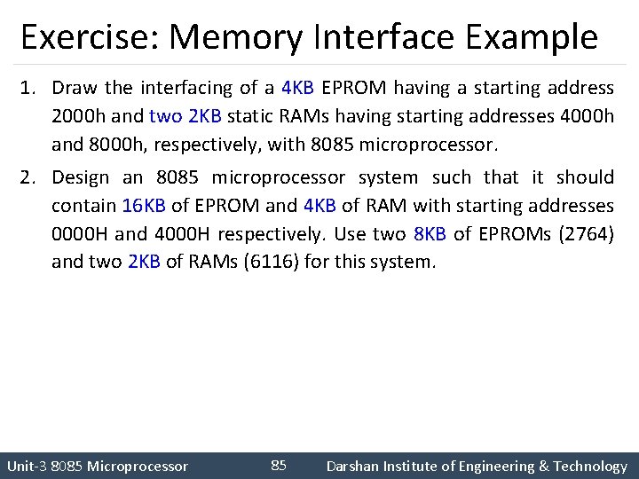
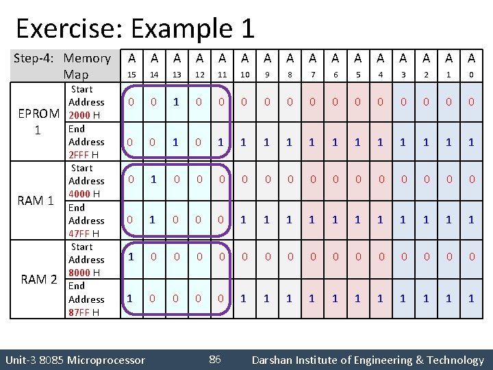
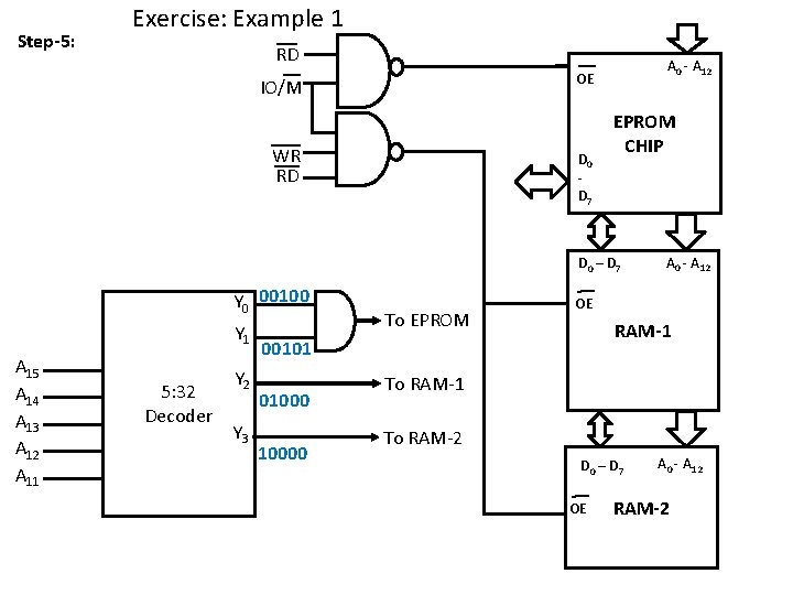
Exercise: Memory Interface Example 1. Draw the interfacing of a 4 KB EPROM having a starting address 2000 h and two 2 KB static RAMs having starting addresses 4000 h and 8000 h, respectively, with 8085 microprocessor. 2. Design an 8085 microprocessor system such that it should contain 16 KB of EPROM and 4 KB of RAM with starting addresses 0000 H and 4000 H respectively. Use two 8 KB of EPROMs (2764) and two 2 KB of RAMs (6116) for this system. 85 Darshan Institute of Engineering & Technology Unit-3 8085 Microprocessor

Exercise: Example 1 Step-4: Memory Map EPROM 1 RAM 2 Start Address 2000 H End Address 2 FFF H Start Address 4000 H End Address 47 FF H Start Address 8000 H End Address 87 FF H A A A A 15 14 13 12 11 10 9 8 7 6 5 4 3 2 1 0 0 0 0 0 1 0 1 1 1 0 1 0 0 0 0 1 0 0 0 1 1 1 0 0 0 0 1 0 0 1 1 1 86 Darshan Institute of Engineering & Technology Unit-3 8085 Microprocessor

Step-5: Exercise: Example 1 RD A 0 - A 12 OE IO/M WR RD D 0 D 7 EPROM CHIP D 0 – D 7 Y 0 00100 Y 1 A 15 A 14 A 13 A 12 A 11 5: 32 Decoder Y 2 Y 3 To EPROM OE RAM-1 00101 010000 A 0 - A 12 To RAM-1 To RAM-2 D 0 – D 7 OE A 0 - A 12 RAM-2

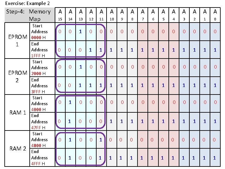
Exercise: Example 2 Step-4: Memory Map EPROM 1 EPROM 2 RAM 1 RAM 2 Start Address 0000 H End Address 1 FFF H Start Address 2000 H End Address 3 FFF H Start Address 4000 H End Address 47 FF H Start Address 4800 H End Address 4 FFF H A A A A 15 14 13 12 11 10 9 8 7 6 5 4 3 2 1 0 0 0 0 0 1 1 1 1 0 0 0 0 0 1 1 1 1 0 1 0 0 0 0 1 0 0 0 1 1 1 0 0 1 0 0 0 1 0 0 1 1 1

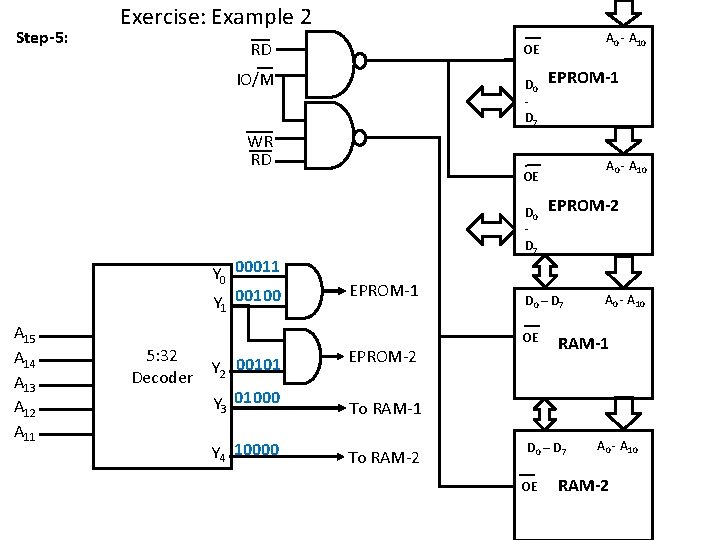
Step-5: Exercise: Example 2 RD IO/M D 0 D 7 WR RD Y 0 00011 Y 00100 1 A 15 A 14 A 13 A 12 A 11 5: 32 Decoder Y 2 00101 A 0 - A 10 OE EPROM-1 A 0 - A 10 OE D 0 D 7 EPROM-1 EPROM-2 Y 3 01000 To RAM-1 Y 4 10000 To RAM-2 EPROM-2 D 0 – D 7 OE RAM-1 D 0 – D 7 OE A 0 - A 10 RAM-2

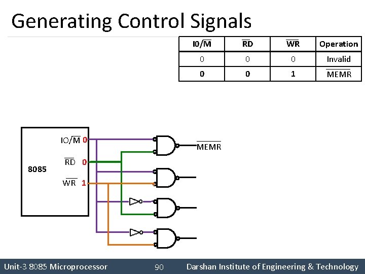
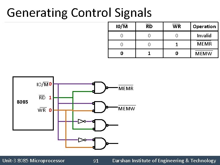
Generating Control Signals IO/M 0 8085 I 0/M RD WR Operation 0 0 0 Invalid 0 0 1 MEMR RD 0 WR 1 Unit-3 8085 Microprocessor 90 Darshan Institute of Engineering & Technology

Generating Control Signals IO/M 0 8085 I 0/M RD WR Operation 0 0 0 1 Invalid MEMR 0 1 0 MEMW MEMR RD 1 WR 0 MEMW Unit-3 8085 Microprocessor 91 Darshan Institute of Engineering & Technology

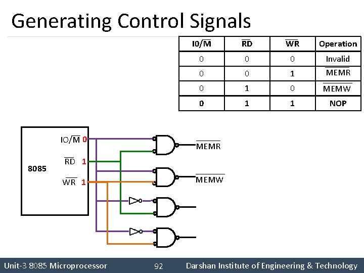
Generating Control Signals IO/M 0 8085 I 0/M RD WR Operation 0 0 0 1 Invalid MEMR 0 1 0 MEMW 0 1 1 NOP MEMR RD 1 WR 1 MEMW Unit-3 8085 Microprocessor 92 Darshan Institute of Engineering & Technology

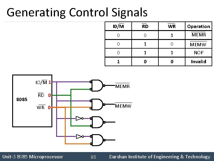
Generating Control Signals IO/M 1 8085 I 0/M RD WR Operation 0 0 1 MEMR 0 1 0 0 1 1 MEMW NOP 1 0 0 Invalid MEMR RD 0 WR 0 MEMW Unit-3 8085 Microprocessor 93 Darshan Institute of Engineering & Technology

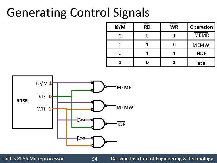
Generating Control Signals IO/M 1 8085 I 0/M RD WR Operation 0 0 1 MEMR 0 1 0 0 1 1 MEMW NOP 1 0 1 IOR MEMR RD 0 WR 1 MEMW IOR Unit-3 8085 Microprocessor 94 Darshan Institute of Engineering & Technology

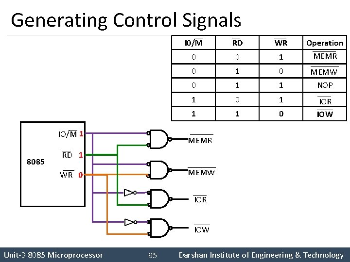
Generating Control Signals IO/M 1 8085 I 0/M RD WR Operation 0 0 1 MEMR 0 1 0 0 1 1 MEMW NOP 1 0 1 1 1 0 IOR IOW MEMR RD 1 WR 0 MEMW IOR IOW Unit-3 8085 Microprocessor 95 Darshan Institute of Engineering & Technology

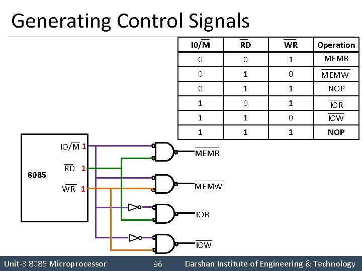
Generating Control Signals IO/M 1 8085 I 0/M RD WR Operation 0 0 1 MEMR 0 1 0 0 1 1 MEMW NOP 1 0 1 1 1 0 IOR IOW 1 1 1 NOP MEMR RD 1 WR 1 MEMW IOR IOW Unit-3 8085 Microprocessor 96 Darshan Institute of Engineering & Technology

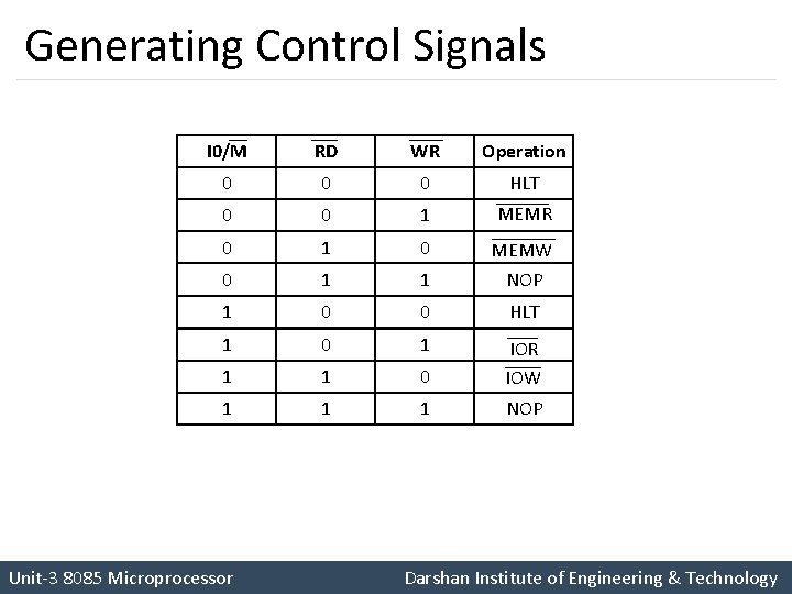
Generating Control Signals I 0/M RD WR Operation 0 0 0 HLT 0 0 1 MEMR 0 1 0 0 1 1 MEMW NOP 1 0 0 HLT 1 0 1 1 1 0 IOR IOW 1 1 1 NOP Unit-3 8085 Microprocessor Darshan Institute of Engineering & Technology