80186 80186 contains 8086 processor and several additional


")
 – When set, it indicates")


- Slides: 28
80186 • 80186 contains 8086 processor and several additional functional chips: – clock generator – 2 independent DMA channels – PIC – 3 programmable 16 -bit timers • more a microcontroller than a microprocessor • used mostly in industrial control applications
Intel 80286
Salient features of 80286 • High performance microprocessor with memory management and protection – 80286 is the first member of the family of advanced microprocessors with builtin/on-chip memory management and protection abilities primarily designed for multi-user/multitasking systems • Available in 12. 5 MHz, 10 MHz & 8 MHz clock frequencies
Salient features of 80286 bus and memory sizes cont… Ø The 80286 CPU, with its 24 -bit address bus is able to address 16 MB of physical memory. Ø 1 GB of virtual memory for each task Microprocessor Data bus width Address bus width Memory size 8086 16 20 1 M 80186 16 20 1 M 80286 16 24 16 M
Salient features of 80286 Operating Modes Intel 80286 has 2 operating modes: Ø Real Address Mode : Ø 80286 is just a fast 8086 --- up to 6 times faster Ø All memory management and protection mechanisms are disabled Ø 286 is object code compatible with 8086 Ø Protected Virtual Address Mode Ø 80286 works with all of its memory management and protection capabilities with the advanced instruction set. Ø it is source code compatible with 8086
Salient features of 80286 cont… Ø 286 includes special instructions to support operating system. Øfor example, one instruction can Øi) ends the current task Øii) save its states Øiii) switch to a new task Øiv) load its states and Øv) begin executing the new task Ø housed in 68 -pin package
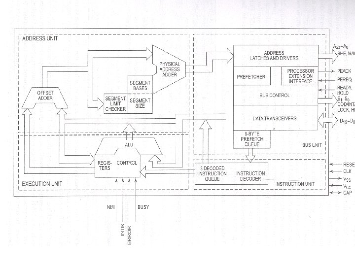
Internal Block Diagram of 80286
EU 8085 BIU 8086 EU AU IU BIU 80286
Functional Parts 1. Address unit 2. Bus unit 3. Instruction unit 4. Execution unit
Address Unit • Calculate the physical addresses of the instruction and data that the CPU want to access • Address lines derived by this unit may be used to address different peripherals. • Physical address computed by the address unit is handed over to the BUS unit.
• • • Bus Unit Performs all memory and I/O read and write operations. Take care of communication between CPU and a coprocessor. Transmit the physical address over address bus A 0 – A 23. Prefetcher module in the bus unit performs this task of prefetching. Bus controller controls the prefetcher module. Fetched instructions are arranged in a 6 – byte prefetch queue.
Instruction Unit • Receive arranged instructions from 6 byte prefetch queue. • • Instruction decoder decodes up to 3 prefetched instruction and are latched them onto a decoded instruction queue. • • Output of the decoding circuit drives a control circuit in the Execution unit.
Execution unit • EU executes the instructions received from the decoded instruction queue sequentially. • Contains Register Bank. • contains one additional special register called Machine status word (MSW) register --- lower 4 bits are only used. • ALU is the heart of execution unit. • After execution ALU sends the result either over data bus or back to the register bank.
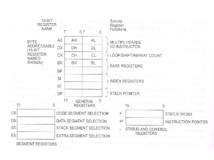
Register organization of 80286 The 80286 CPU contains the same set of registers, as in 8086. 1. Eight 16 -bit general purpose registers. 2. Four 16 bit segment registers. 3. Status and control register. 4. Instruction pointer.
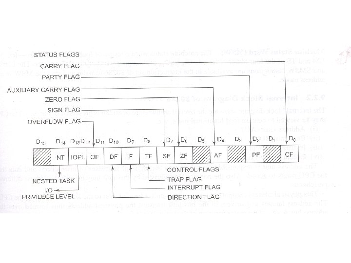
Flag Registers
Ø IOPL – Input Output Privilege Level flags (bit D 12 and D 13) – IOPL is used in protected mode operation to select the privilege level for I/O devices. IF the current privilege level is higher or more trusted than the IOPL, I/O executed without hindrance. If the IOPL is lover than the current privilege level, an interrupt occurs, causing execution to suspend. Note that IPOL 00 is the highest or more trusted; and IOPL 11 is the lowest or least trusted.
Ø NT – Nested task flag (bit D 14) – When set, it indicates that one system task has invoked another through a CALL instruction as opposed to a JMP. For multitasking this can be manipulated to our advantage
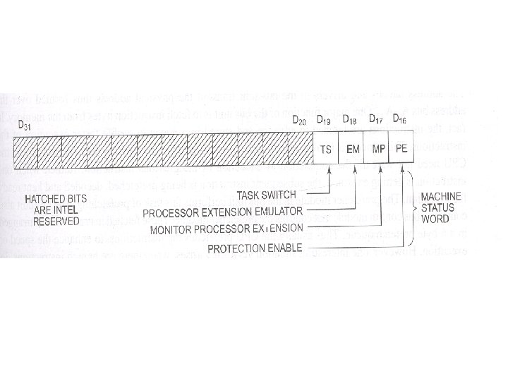
Machine Status Word • Consist of four flags. These are – PE, MP, EM and TS • LMSW & SMSW instruction are available in the instruction set of 80286 to write and read the MSW in real address mode.
Ø PE - Protection enable Ø Protection enable flag places the 80286 in protected mode, if set. This can only be cleared by resetting the CPU. Ø MP – Monitor processor extension Ø flag allows WAIT instruction to generate a processor extension. Ø EM – Emulate processor extension flag, Ø if set , causes a processor extension absent exception and permits the emulation of processor extension by CPU. Ø TS – Task switch Ø if set this flag indicates the next instruction using extension will generate exception 7, permitting the CPU to test whether the current processor extension is for current task.
Additional Instructions of Intel 80286 Sl no 1. Instruction Purpose CLTS Clear the task – switched bit 2. LDGT Load global descriptor table register 3. SGDT Store global descriptor table register 4. LIDT Load interrupt descriptor table register 5. SIDT Store interrupt descriptor table register 6. LLDT Load local descriptor table register 7. SLDT Store local descriptor table register 8. LMSW Load machine status register 9. SMSW Store machine status register
Sl no Instruction Purpose 10. LAR Load access rights 11. LSL Load segment limit 12. SAR Store access right 13. ARPL Adjust requested privilege level 14. VERR Verify a read access 15. VERW Verify a write access
Ø CLTS Ø The clear task – switched flag instruction clears the TS (Task - switched) flag bit to a logic 0. Ø LAR Ø The load access rights Instruction reads the segment descriptor and place a copy of the access rights byte into a 16 bit register. Ø LSL Ø The load segment limit instruction Loads a user – specified register with the segment limit.
Ø VERR Ø The verify for read access instruction verifies that a segment can de read. Ø VERW Ø The verify for write access instruction is used to verify that a segment can be written. Ø ARPL Ø The Adjust request privilege level instruction is used to test a selector so that the privilege level of the requested selector is not violated.
THAT’S ALL FOR TODAY