An Introduction to 8086 Microprocessor History of Intels


 – 5. 5 million Trs")


 and")

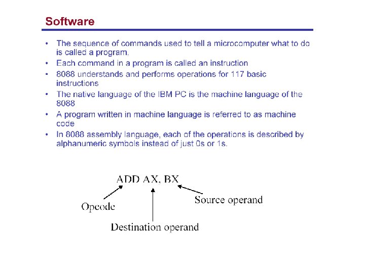
 EU")
 AX, BX, CX and DX are")


 address is a combination of")


 Indicates overflow of the leftmost bit during arithmetic. •")
 Contains the resulting sign of an arithmetic operation (1=negative) •")
- Slides: 40
An Introduction to 8086 Microprocessor.
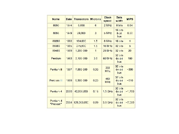
History of Intel’s Microprocessors • • Intel 4004 – 1971, 4 -bit Intel 8008 – 1972, 8 -bit – Originally designed for Datapoint Corp. as a CRT display controller Intel 8080 – 1974, April - Altair 8800, 1975, MITS( 256 bytes of Mem, $395) – Apple II -- Steve Jobs and Steve Wozniak 1976, Apple 사 설립 – Bill Gates and a fellow student : BASIC, 1975 --> Microsoft Intel 8086/8088 – 1978, 16 bit: 8088, 1979, 8 -bit external bus
• • – IBM PC ; 1981 – 29, 000 Trs Intel 80286 – 1982, 16 -bit architecture – 24 -bit addressing, memory protection and virtual memory – 16 MB of physical MEM and 1 GB of virtual mem – 130, 000 Trs onto a single chip – IBM PC/AT in 1984, IBM PS/2 Model 50 and 60 Intel 80386 – 1985, 32 bits – 3~5 MIPS (7 MIPS on the 25 MHz chip) – memory paging and enhanced I/O permission features – 4 GB programming model
• • Intel 80486 – 1989 Spring COMDEX show -> 1990 June : actual release – 1, 200, 000 Trs – 386+387+8 K data and instruction cache, paging and MMU Pentium – 1993 – 110 MIPS on 66 Mhz Chip – 16 KB on-chip cache and 64 bit data bus – superscalar technology (two instructions/clock) – 3. 1 million transistors
• • Pentium Pro – 1995, Superscalar(three-way issue) – 5. 5 million Trs in the CPU core + 15. 5 million Trs in the secondary cache 8 K data, 8 K instr cache – 256 KB SRAM secondary cache – 200 SPECint 92 at 133 MHz – 2. 9 V, 0. 6 micron BICMOS Pentium II – Pentium Pro + MMX, 1997 – 233, 266, upto 450 MHz – 7. 5 million Trs in CPU – 512 KB in secondary cache
• Pentium III – 1999 – Pentium Pro + MMX + Internet Streaming SIMD Instructions – 0. 25 micron, 9. 5 million Trs – 600 MHz, 550 MHz, . . . – 32 K(16 K/16 K) non-blocking level 1 cache
8086 Microprocessor
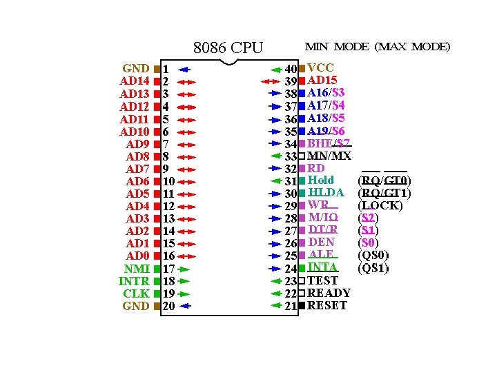
8086 Features • 16 -bit Arithmetic Logic Unit • 16 -bit data bus (8088 has 8 -bit data bus) • 20 -bit address bus - 220 = 1, 048, 576 = 1 meg The address refers to a byte in memory. In the 8088, these bytes come in on the 8 -bit data bus. In the 8086, bytes at even addresses come in on the low half of the data bus (bits 0 -7) and bytes at odd addresses come in on the upper half of the data bus (bits 8 -15). The 8086 can read a 16 -bit word at an even address in one operation and at an odd address in two operations. The 8088 needs two operations in either case. The least significant byte of a word on an 8086 family microprocessor is at the lower address.
Simplified CPU Design
Intel 16 -bit Registers
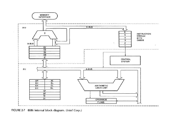
8086 Architecture • The 8086 has two parts, the Bus Interface Unit (BIU) and the Execution Unit (EU). • The BIU fetches instructions, reads and writes data, and computes the 20 -bit address. • The EU decodes and executes the instructions using the 16 -bit ALU. • The BIU contains the following registers: IP - the Instruction Pointer CS - the Code Segment Register DS - the Data Segment Register SS - the Stack Segment Register ES - the Extra Segment Register The BIU fetches instructions using the CS and IP, written CS: IP, to contract the 20 -bit address. Data is fetched using a segment register (usually the DS) and an effective address (EA) computed by the EU depending on the addressing mode.
The EU contains the following 16 -bit registers: AX - the Accumulator BX - the Base Register CX - the Count Register DX - the Data Register SP - the Stack Pointer defaults to stack segment BP - the Base Pointer / SI - the Source Index Register DI - the Destination Register These are referred to as general-purpose registers, although, as seen by their names, they often have a special-purpose use for some instructions. The AX, BX, CX, and DX registers can be considers as two 8 -bit registers, a High byte and a Low byte. This allows byte operations and compatibility with the previous generation of 8 -bit processors, the 8080 and 8085 source code could be translated in 8086 code and assembled. The 8 -bit registers are: AX --> AH, AL BX --> BH, BL CX --> CH, CL DX --> DH, DL
8086 Programmer’s Model ES CS SS DS IP BIU registers (20 bit adder) EU registers AX BX CX DX AH BH CH DH Extra Segment Code Segment Stack Segment Data Segment Instruction Pointer AL BL CL DL SP BP SI DI FLAGS Accumulator Base Register Count Register Data Register Stack Pointer Base Pointer Source Index Register Destination Index Register
8086/88 internal registers 16 bits (2 bytes each) AX, BX, CX and DX are two bytes wide and each byte can be accessed separately These registers are used as memory pointers. Flags will be discussed later Segment registers are used as base address for a segment in the 1 M byte of memory
The 8086/8088 Microprocessors: Registers • Registers – Registers are in the CPU and are referred to by specific names – Data registers • Hold data for an operation to be performed • There are 4 data registers (AX, BX, CX, DX) – Address registers • • Hold the address of an instruction or data element Segment registers (CS, DS, ES, SS) Pointer registers (SP, BP, IP) Index registers (SI, DI) – Status register • Keeps the current status of the processor • On an IBM PC the status register is called the FLAGS register – In total there are fourteen 16 -bit registers in an 8086/8088
Data Registers: AX, BX, CX, DX • Instructions execute faster if the data is in a register • AX, BX, CX, DX are the data registers • Low and High bytes of the data registers can be accessed separately – AH, BH, CH, DH are the high bytes – AL, BL, CL, and DL are the low bytes • Data Registers are general purpose registers but they also perform special functions • AX – Accumulator Register – Preferred register to use in arithmetic, logic and data transfer instructions because it generates the shortest Machine Language Code – Must be used in multiplication and division operations – Must also be used in I/O operations
• BX – – Base Register Also serves as an address register Used in array operations Used in Table Lookup operations (XLAT) • CX – Count register – Used as a loop counter – Used in shift and rotate operations • DX – Data register – Used in multiplication and division – Also used in I/O operations
Pointer and Index Registers • Contain the offset addresses of memory locations • Can also be used in arithmetic and other operations • SP: Stack pointer – Used with SS to access the stack segment • BP: Base Pointer – Primarily used to access data on the stack – Can be used to access data in other segments • SI: Source Index register – is required for some string operations – When string operations are performed, the SI register points to memory locations in the data segment which is addressed by the DS register. Thus, SI is associated with the DS in string operations.
• DI: Destination Index register – is also required for some string operations. – When string operations are performed, the DI register points to memory locations in the data segment which is addressed by the ES register. Thus, DI is associated with the ES in string operations. • The SI and the DI registers may also be used to access data stored in arrays
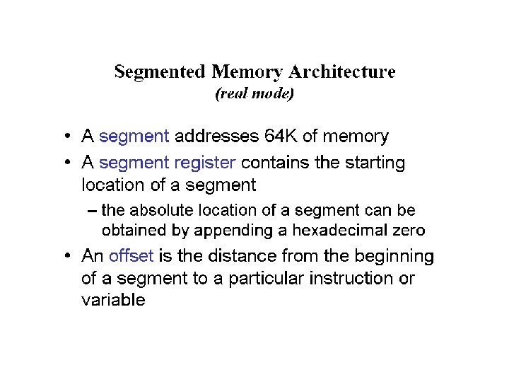
Segment Registers - CS, DS, SS and ES • Are Address registers • Store the memory addresses of instructions and data • Memory Organization – Each byte in memory has a 20 bit address starting with 0 to 220 -1 or 1 meg of addressable memory – Addresses are expressed as 5 hex digits from 00000 - FFFFF – Problem: But 20 bit addresses are TOO BIG to fit in 16 bit registers! – Solution: Memory Segment • • • Block of 64 K (65, 536) consecutive memory bytes A segment number is a 16 bit number Segment numbers range from 0000 to FFFF Within a segment, a particular memory location is specified with an offset An offset also ranges from 0000 to FFFF
Segmented Memory linear addresses Segmented memory addressing: absolute (linear) address is a combination of a 16 -bit segment value added to a 16 -bit offset one segment
Intel Memory Address Generation • The BIU has a dedicated adder for determining physical memory addresses Offset Value (16 bits) Segment Register (16 bits) 0000 Adder Physical Address (20 Bits)
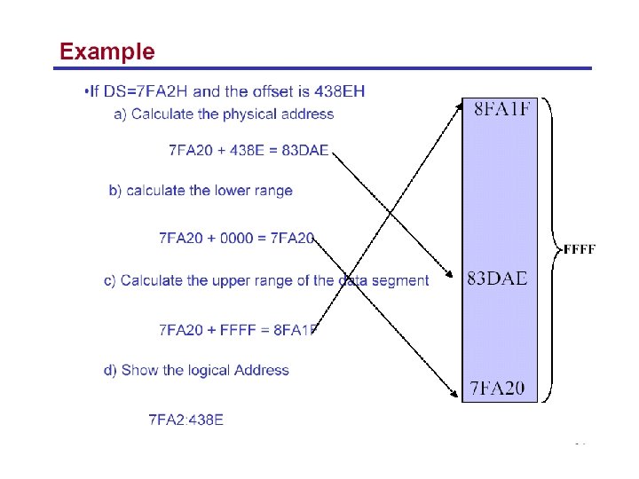
Intel Example Address Calculation • If the data segment starts at location 1000 h and a data reference contains the address 29 h where is the actual data? 2 9 Offset: 00000101001 Segment: 0001000000 Address: 00010000010 1001
Segment: Offset Address • Logical Address is specified as segment: offset • Physical address is obtained by shifting the segment address 4 bits to the left and adding the offset address • Thus the physical address of the logical address A 4 FB: 4872 is A 4 FB 0 + 4872 A 9822
Your turn. . . What linear address corresponds to the segment/offset address 028 F: 0030? 028 F 0 + 0030 = 02920 Always use hexadecimal notation for addresses.
Your turn. . . What segment addresses correspond to the linear address 28 F 30 h? Many different segment-offset addresses can produce the linear address 28 F 30 h. For example: 28 F 0: 0030, 28 F 3: 0000, 28 B 0: 0430, . . .
The Code Segment 0 H CS: 4000 H 0400 H IP 0400 0 Segment Register + Offset Physical or Absolute Address 4056 H 0056 H CS: IP = 400: 56 Logical Address Memory 0056 04056 H 0 FFFFFH The offset is the distance in bytes from the start of the segment. The offset is given by the IP for the Code Segment. Instructions are always fetched with using the CS register. The physical address is also called the absolute address.
The Data Segment 0 H DS: 05 C 00 H 05 C 0 EA 0050 05 C 0 Segment Register + Offset Physical Address 05 C 50 H DS: EA 0 Memory 0050 05 C 50 H 0 FFFFFH Data is usually fetched with respect to the DS register. The effective address (EA) is the offset. The EA depends on the addressing mode.
The Stack Segment 0 H SS: 0 A 000 H 0 A 00 SP 0100 0 A 00 0 Segment Register Offset Physical Address + 0 A 100 H SS: SP Memory 0100 0 A 100 H 0 FFFFFH The offset is given by the SP register. The stack is always referenced with respect to the stack segment register. The stack grows toward decreasing memory locations. The SP points to the last or top item on the stack. PUSH - pre-decrement the SP POP - post-increment the SP
Flags Carry flag Overflow Parity flag Direction Interrupt enable Auxiliary flag Trap 6 are status flags 3 are control flag Zero Sign
Flag Register • Conditional flags: – They are set according to some results of arithmetic operation. You do not need to alter the value yourself. • Control flags: – Used to control some operations of the MPU. These flags are to be set by you in order to achieve some specific purposes. Flag Bit no. 15 14 13 12 O D I T S Z 11 10 9 8 7 6 A 5 4 P 3 2 C 1 • CF (carry) Contains carry from leftmost bit following arithmetic, also contains last bit from a shift or rotate operation. 0
Flag Register • OF (overflow) Indicates overflow of the leftmost bit during arithmetic. • DF (direction) Indicates left or right for moving or comparing string data. • IF (interrupt) Indicates whether external interrupts are being processed or ignored. • TF (trap) Permits operation of the processor in single step mode.
• SF (sign) Contains the resulting sign of an arithmetic operation (1=negative) • ZF (zero) Indicates when the result of arithmetic or a comparison is zero. (1=yes) • AF (auxiliary carry) Contains carry out of bit 3 into bit 4 for specialized arithmetic. • PF (parity) Indicates the number of 1 bits that result from an operation.