The M 68000 Processor ECE 511 Digital System












- Slides: 92

The M 68000 Processor ECE 511: Digital System & Microprocessor

What we are going to learn in this session: n M 68 k hardware architecture: ¨ M 68 k pin assignments ¨ Pin functions.

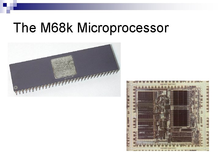
The M 68 k Microprocessor M 68000, M 68 k microprocessor. n Motorola Semiconductors, 1979. n 16 -bit processor, but can perform 32 -bit operations. n Speed: 8 -12 MHz. n

The M 68 k Microprocessor n Very advanced compared to 8 -bit processors: ¨ 16 -bit data bus, 24 -bit address bus. ¨ Can execute instructions twice as fast. n Still available today: ¨ Simple, practical commands. ¨ Robust: can be used for many applications.

The M 68 k Microprocessor

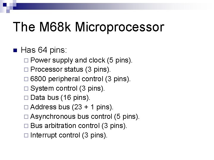
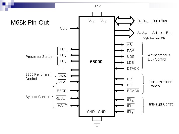
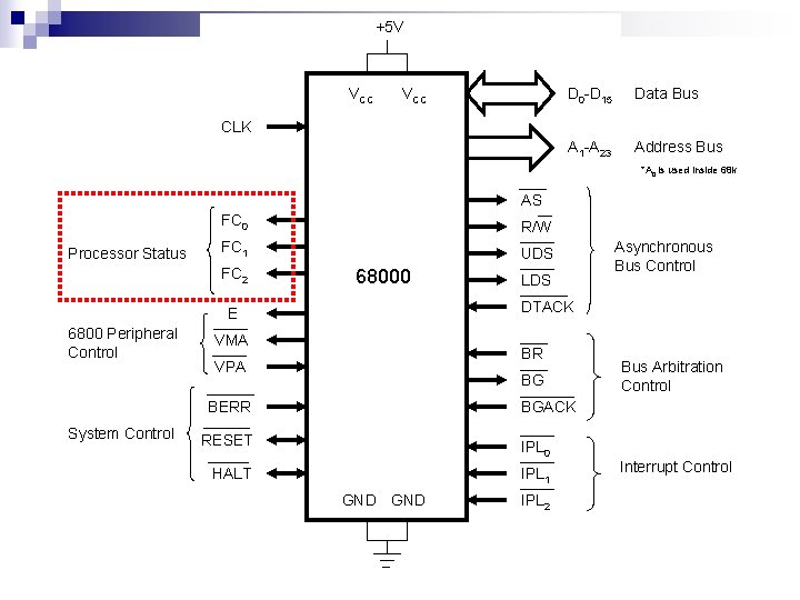
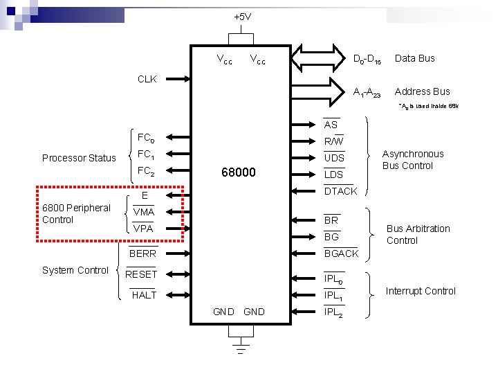
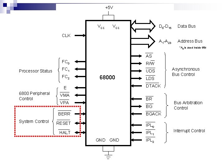
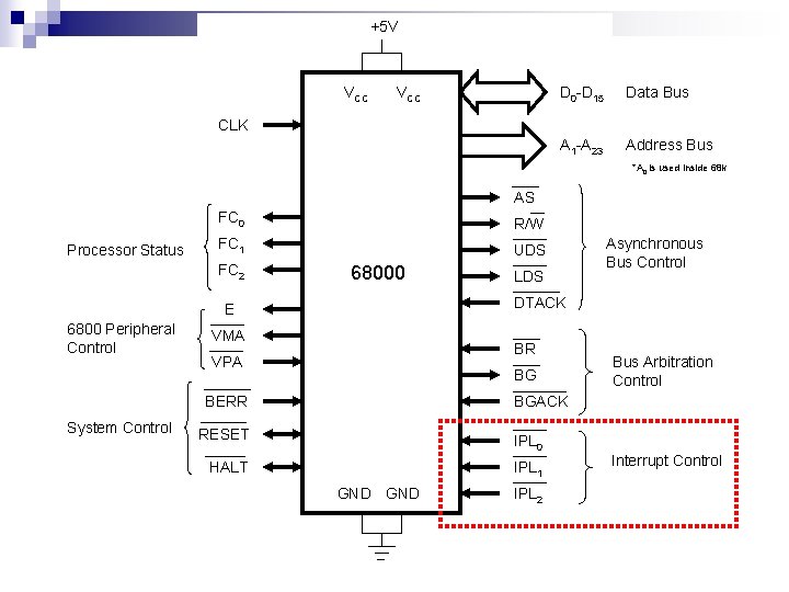
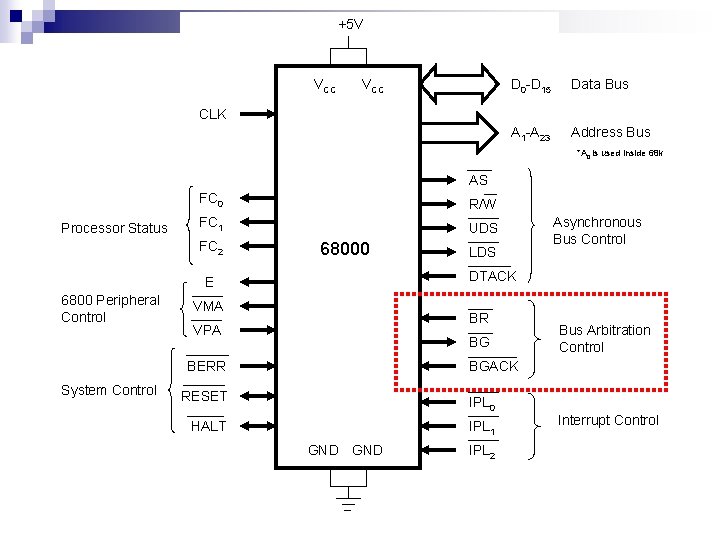
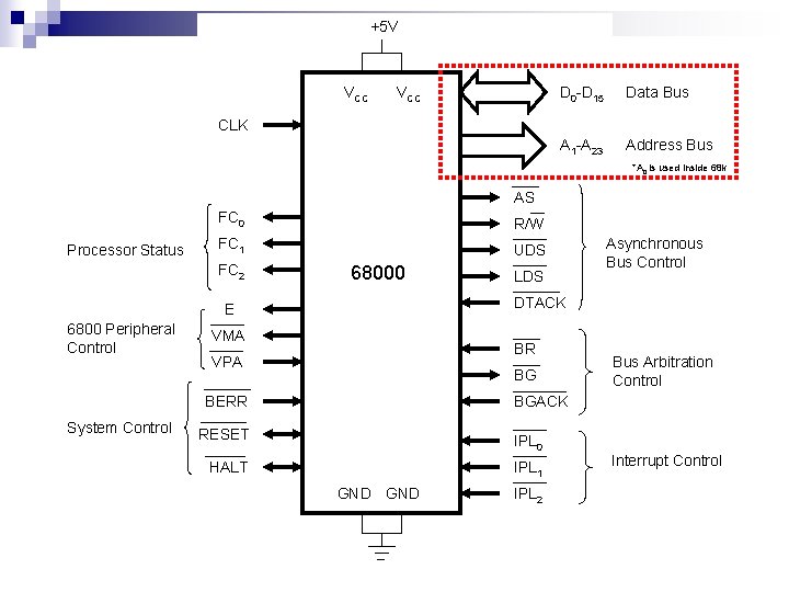
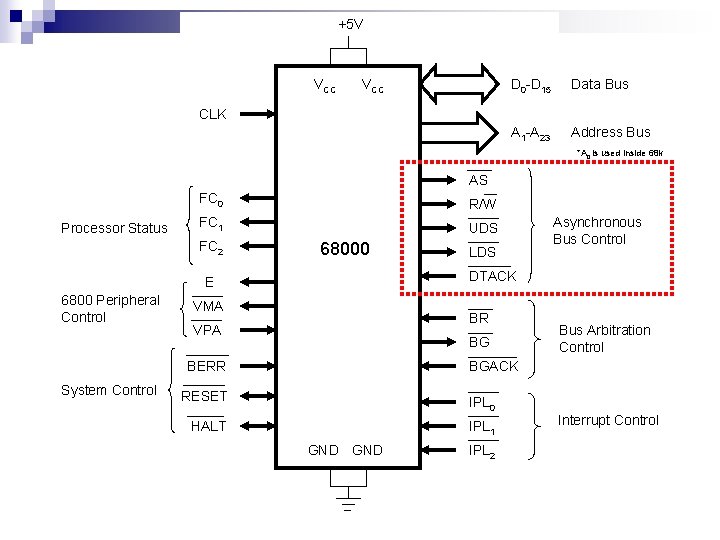
The M 68 k Microprocessor n Has 64 pins: ¨ Power supply and clock (5 pins). ¨ Processor status (3 pins). ¨ 6800 peripheral control (3 pins). ¨ System control (3 pins). ¨ Data bus (16 pins). ¨ Address bus (23 + 1 pins). ¨ Asynchronous bus control (5 pins). ¨ Bus arbitration control (3 pins). ¨ Interrupt control (3 pins).

+5 V VCC M 68 k Pin-Out VCC D 0 -D 15 Data Bus A 1 -A 23 Address Bus CLK *A 0 is used inside 68 k AS Processor Status FC 0 R/W FC 1 UDS FC 2 68000 DTACK E 6800 Peripheral Control VMA BR VPA BG BERR System Control LDS Asynchronous Bus Control Bus Arbitration Control BGACK RESET IPL 0 HALT IPL 1 GND IPL 2 Interrupt Control

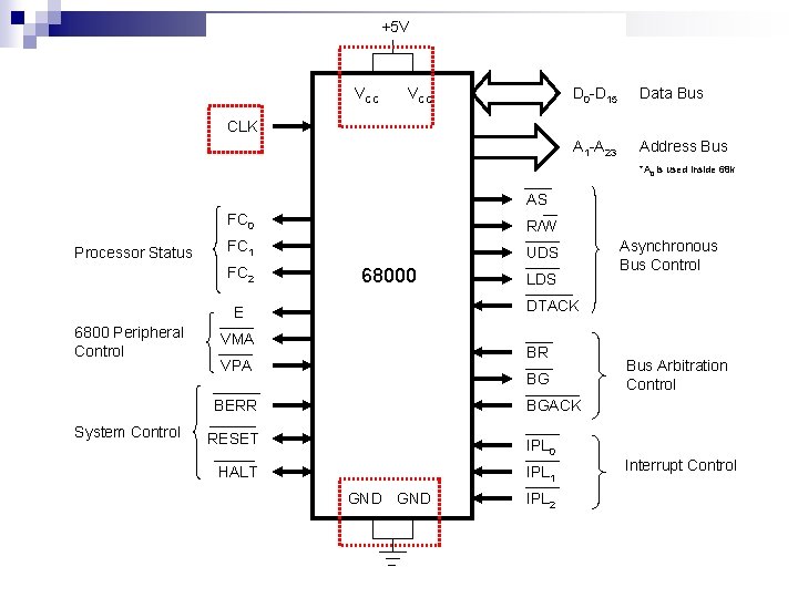
Power Supply & Clock

+5 V VCC D 0 -D 15 Data Bus A 1 -A 23 Address Bus CLK *A 0 is used inside 68 k AS Processor Status FC 0 R/W FC 1 UDS FC 2 68000 DTACK E 6800 Peripheral Control VMA BR VPA BG BERR System Control LDS Asynchronous Bus Control Bus Arbitration Control BGACK RESET IPL 0 HALT IPL 1 GND IPL 2 Interrupt Control

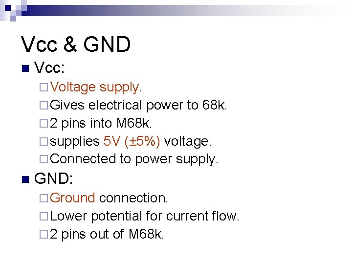
Vcc & GND n Vcc: ¨ Voltage supply. ¨ Gives electrical power to 68 k. ¨ 2 pins into M 68 k. ¨ supplies 5 V (± 5%) voltage. ¨ Connected to power supply. n GND: ¨ Ground connection. ¨ Lower potential for current flow. ¨ 2 pins out of M 68 k.

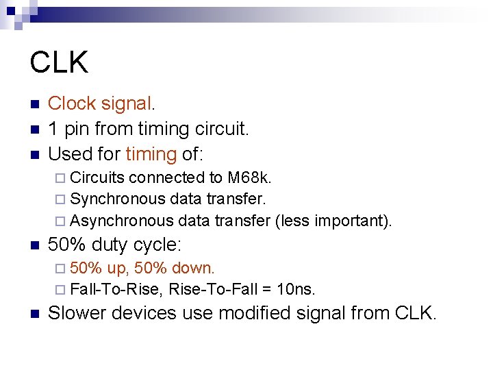
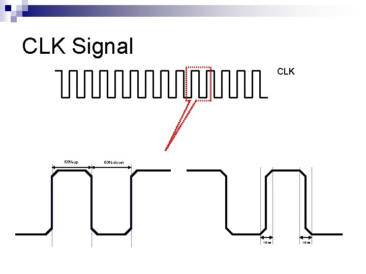
CLK n n n Clock signal. 1 pin from timing circuit. Used for timing of: ¨ Circuits connected to M 68 k. ¨ Synchronous data transfer. ¨ Asynchronous data transfer (less important). n 50% duty cycle: ¨ 50% up, 50% down. ¨ Fall-To-Rise, Rise-To-Fall = 10 ns. n Slower devices use modified signal from CLK.

CLK Signal CLK 50% up 50% down 10 ns

Processor Status Pins

+5 V VCC D 0 -D 15 Data Bus A 1 -A 23 Address Bus CLK *A 0 is used inside 68 k AS Processor Status FC 0 R/W FC 1 UDS FC 2 68000 DTACK E 6800 Peripheral Control VMA BR VPA BG BERR System Control LDS Asynchronous Bus Control Bus Arbitration Control BGACK RESET IPL 0 HALT IPL 1 GND IPL 2 Interrupt Control

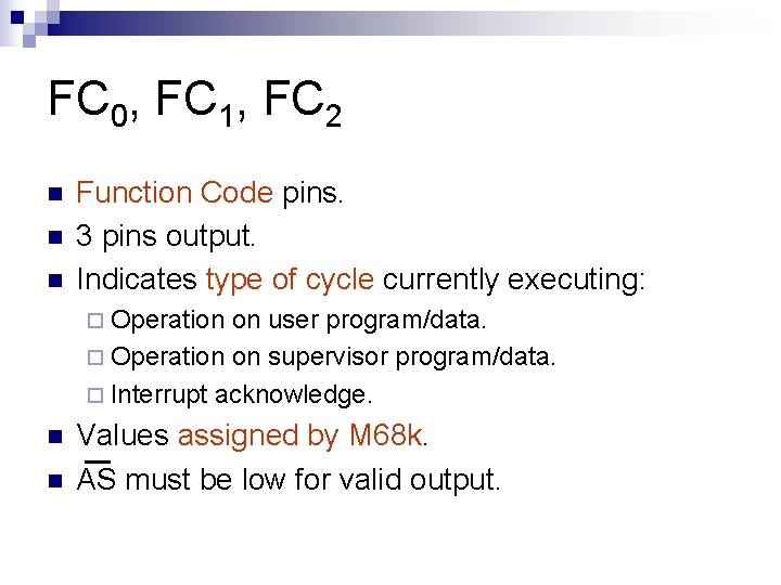
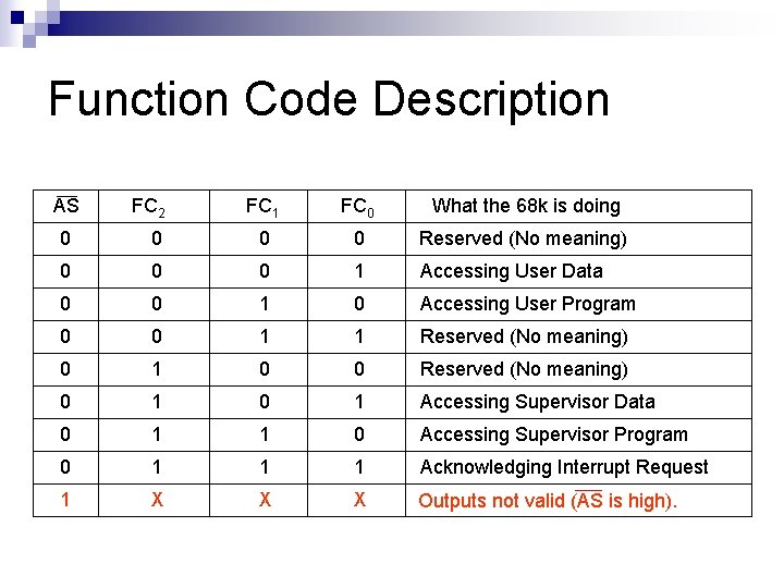
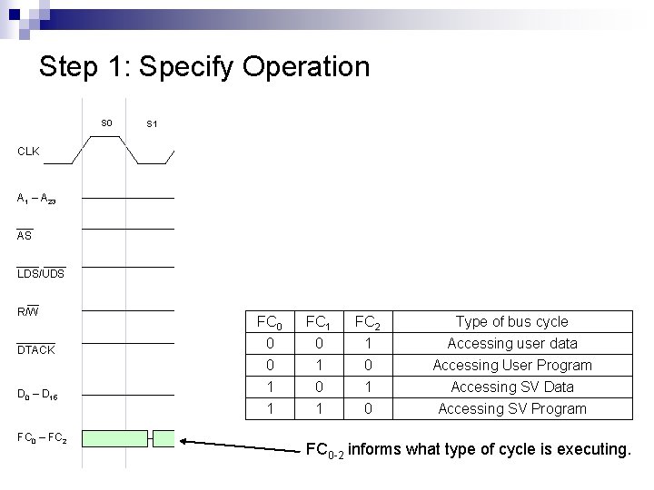
FC 0, FC 1, FC 2 n n n Function Code pins. 3 pins output. Indicates type of cycle currently executing: ¨ Operation on user program/data. ¨ Operation on supervisor program/data. ¨ Interrupt acknowledge. n n Values assigned by M 68 k. AS must be low for valid output.

Function Code Description AS FC 2 FC 1 FC 0 What the 68 k is doing 0 0 Reserved (No meaning) 0 0 0 1 Accessing User Data 0 0 1 0 Accessing User Program 0 0 1 1 Reserved (No meaning) 0 1 0 0 Reserved (No meaning) 0 1 Accessing Supervisor Data 0 1 1 0 Accessing Supervisor Program 0 1 1 1 Acknowledging Interrupt Request 1 X X X Outputs not valid (AS is high).

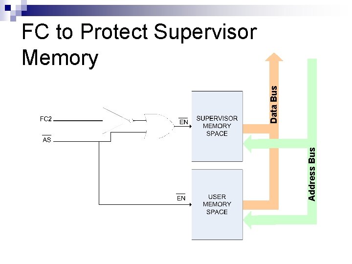
Address Bus Data Bus FC to Protect Supervisor Memory

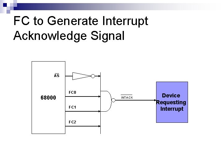
FC to Generate Interrupt Acknowledge Signal AS 68000 FC 0 INTACK FC 1 FC 2 Device Requesting Interrupt

6800 Peripheral Control

+5 V VCC D 0 -D 15 Data Bus A 1 -A 23 Address Bus CLK *A 0 is used inside 68 k AS Processor Status FC 0 R/W FC 1 UDS FC 2 68000 DTACK E 6800 Peripheral Control VMA BR VPA BG BERR System Control LDS Asynchronous Bus Control Bus Arbitration Control BGACK RESET IPL 0 HALT IPL 1 GND IPL 2 Interrupt Control

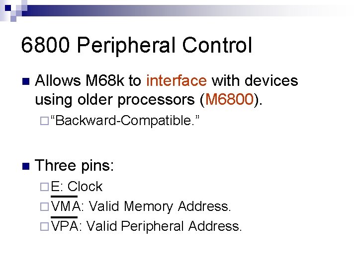
6800 Peripheral Control n Allows M 68 k to interface with devices using older processors (M 6800). ¨ “Backward-Compatible. ” n Three pins: ¨ E: Clock ¨ VMA: Valid Memory Address. ¨ VPA: Valid Peripheral Address.

Synchronous Data Exchange n Mode where: ¨ Data exchange performed using same timing. ¨ Timing generated by single clock signal. ¨ Shared by all synchronous devices.

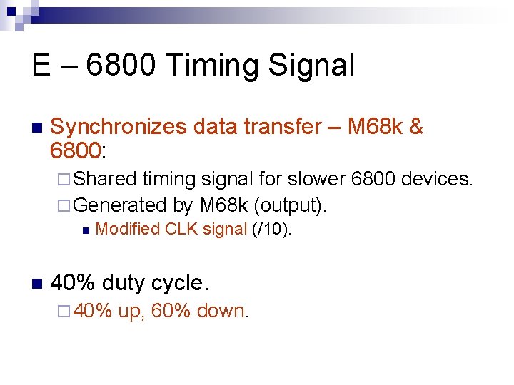
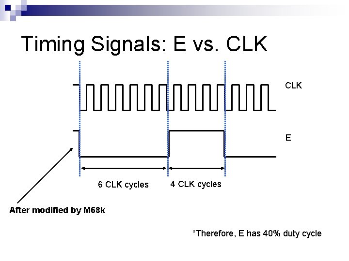
E – 6800 Timing Signal n Synchronizes data transfer – M 68 k & 6800: ¨ Shared timing signal for slower 6800 devices. ¨ Generated by M 68 k (output). n n Modified CLK signal (/10). 40% duty cycle. ¨ 40% up, 60% down.

Timing Signals: E vs. CLK E 6 CLK cycles 4 CLK cycles After modified by M 68 k *Therefore, E has 40% duty cycle

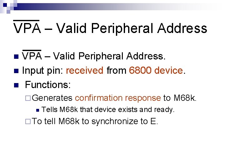
VPA – Valid Peripheral Address. n Input pin: received from 6800 device. n Functions: n ¨ Generates n confirmation response to M 68 k. Tells M 68 k that device exists and ready. ¨ To tell M 68 k to synchronize to E.

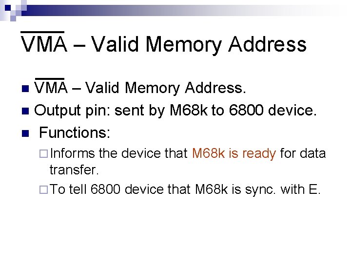
VMA – Valid Memory Address. n Output pin: sent by M 68 k to 6800 device. n Functions: n ¨ Informs the device that M 68 k is ready for data transfer. ¨ To tell 6800 device that M 68 k is sync. with E.

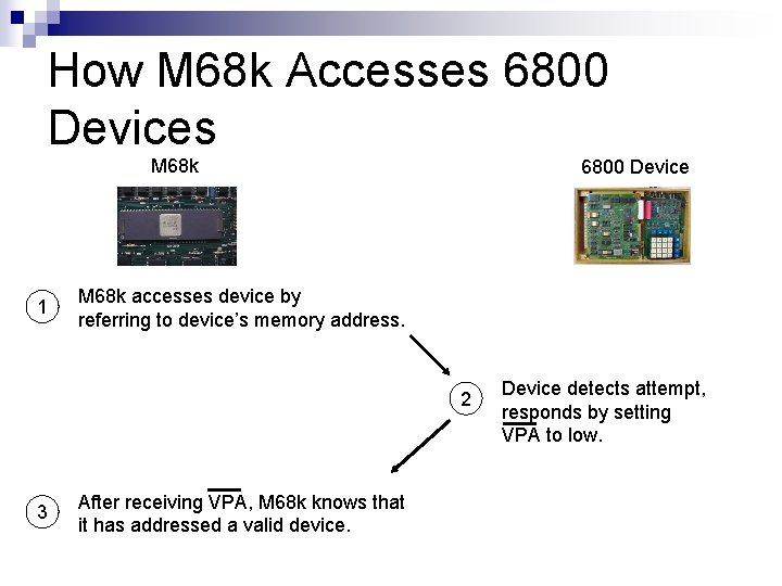
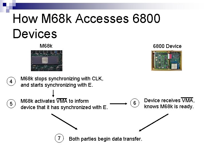
How M 68 k Accesses 6800 Devices M 68 k 1 6800 Device M 68 k accesses device by referring to device’s memory address. 2 3 After receiving VPA, M 68 k knows that it has addressed a valid device. Device detects attempt, responds by setting VPA to low.

How M 68 k Accesses 6800 Devices M 68 k 6800 Device 4 M 68 k stops synchronizing with CLK, and starts synchronizing with E. 5 M 68 k activates VMA to inform device that it has synchronized with E. 7 6 Both parties begin data transfer. Device receives VMA, knows M 68 k is ready.

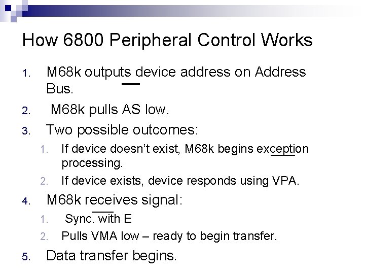
How 6800 Peripheral Control Works 1. 2. 3. M 68 k outputs device address on Address Bus. M 68 k pulls AS low. Two possible outcomes: 1. 2. 4. M 68 k receives signal: 1. 2. 5. If device doesn’t exist, M 68 k begins exception processing. If device exists, device responds using VPA. Sync. with E Pulls VMA low – ready to begin transfer. Data transfer begins.

System Control

+5 V VCC D 0 -D 15 Data Bus A 1 -A 23 Address Bus CLK *A 0 is used inside 68 k AS Processor Status FC 0 R/W FC 1 UDS FC 2 68000 DTACK E 6800 Peripheral Control VMA BR VPA BG BERR System Control LDS Asynchronous Bus Control Bus Arbitration Control BGACK RESET IPL 0 HALT IPL 1 GND IPL 2 Interrupt Control

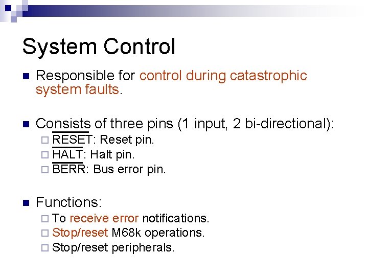
System Control n Responsible for control during catastrophic system faults. n Consists of three pins (1 input, 2 bi-directional): ¨ RESET: Reset pin. ¨ HALT: Halt pin. ¨ BERR: Bus error pin. n Functions: ¨ To receive error notifications. ¨ Stop/reset M 68 k operations. ¨ Stop/reset peripherals.

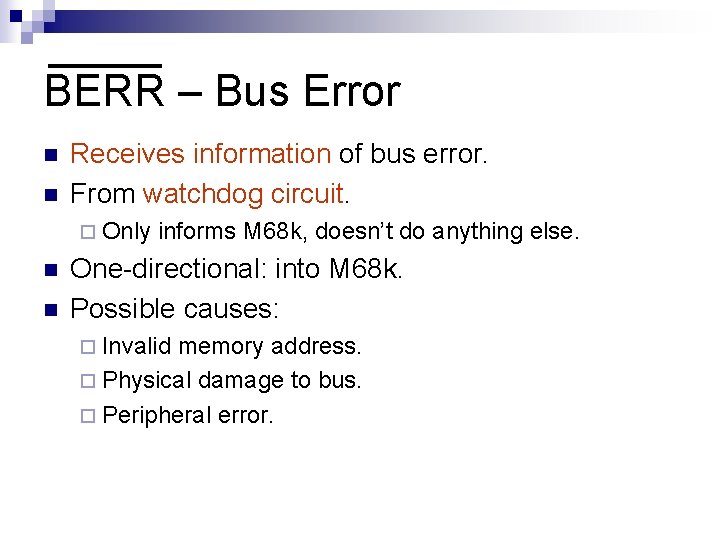
BERR – Bus Error n n Receives information of bus error. From watchdog circuit. ¨ Only n n informs M 68 k, doesn’t do anything else. One-directional: into M 68 k. Possible causes: ¨ Invalid memory address. ¨ Physical damage to bus. ¨ Peripheral error.

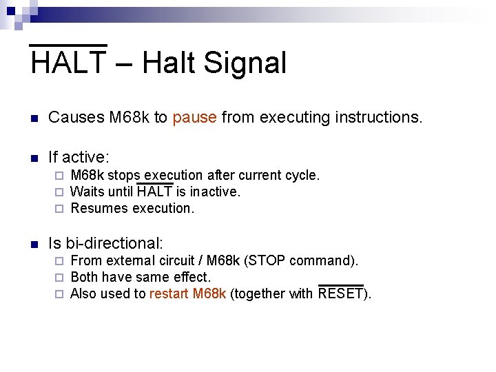
HALT – Halt Signal n Causes M 68 k to pause from executing instructions. n If active: ¨ ¨ ¨ n M 68 k stops execution after current cycle. Waits until HALT is inactive. Resumes execution. Is bi-directional: ¨ ¨ ¨ From external circuit / M 68 k (STOP command). Both have same effect. Also used to restart M 68 k (together with RESET).

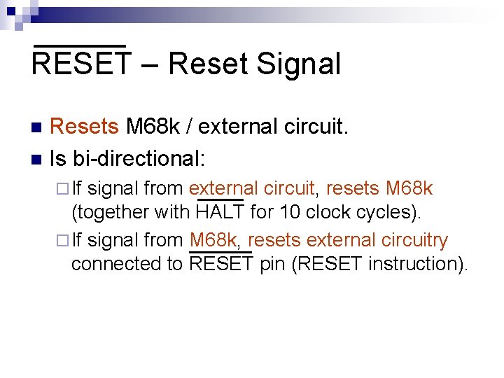
RESET – Reset Signal Resets M 68 k / external circuit. n Is bi-directional: n ¨ If signal from external circuit, resets M 68 k (together with HALT for 10 clock cycles). ¨ If signal from M 68 k, resets external circuitry connected to RESET pin (RESET instruction).

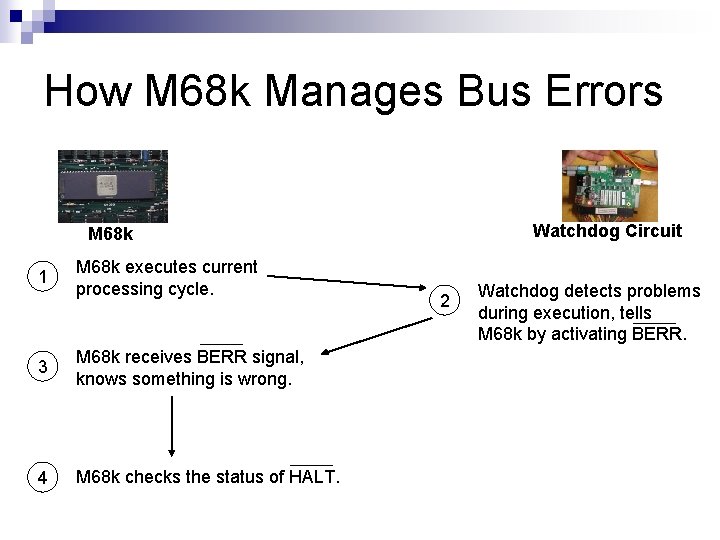
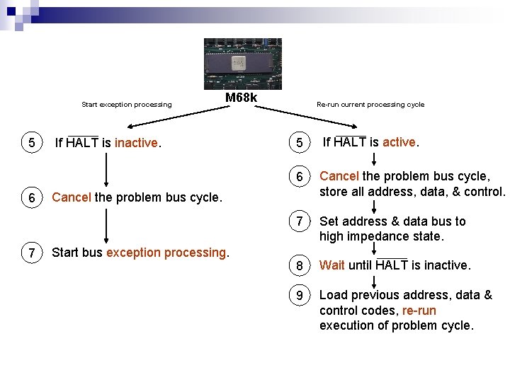
How M 68 k Manages Bus Errors Watchdog Circuit M 68 k 1 M 68 k executes current processing cycle. 3 M 68 k receives BERR signal, knows something is wrong. 4 M 68 k checks the status of HALT. 2 Watchdog detects problems during execution, tells M 68 k by activating BERR.

Start exception processing 5 6 7 M 68 k If HALT is inactive. Re-run current processing cycle 5 If HALT is active. 6 Cancel the problem bus cycle, store all address, data, & control. 7 Set address & data bus to high impedance state. 8 Wait until HALT is inactive. 9 Load previous address, data & control codes, re-run execution of problem cycle. Cancel the problem bus cycle. Start bus exception processing.

Interrupt Control

+5 V VCC D 0 -D 15 Data Bus A 1 -A 23 Address Bus CLK *A 0 is used inside 68 k AS Processor Status FC 0 R/W FC 1 UDS FC 2 68000 DTACK E 6800 Peripheral Control VMA BR VPA BG BERR System Control LDS Asynchronous Bus Control Bus Arbitration Control BGACK RESET IPL 0 HALT IPL 1 GND IPL 2 Interrupt Control

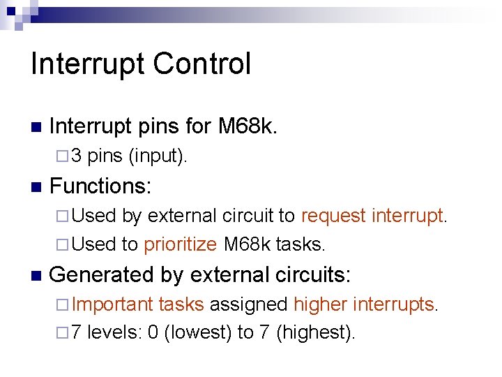
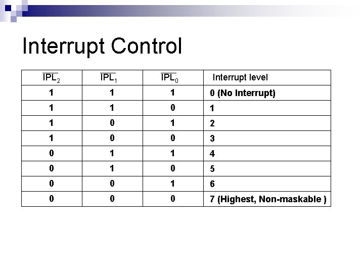
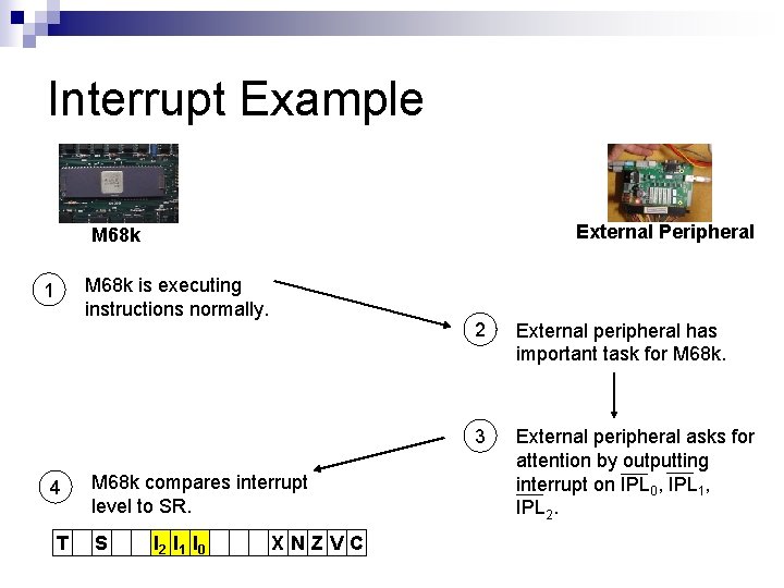
Interrupt Control n Interrupt pins for M 68 k. ¨ 3 n pins (input). Functions: ¨ Used by external circuit to request interrupt. ¨ Used to prioritize M 68 k tasks. n Generated by external circuits: ¨ Important tasks assigned higher interrupts. ¨ 7 levels: 0 (lowest) to 7 (highest).

Interrupt Control IPL 2 IPL 1 IPL 0 Interrupt level 1 1 1 0 (No Interrupt) 1 1 0 1 2 1 0 0 3 0 1 1 4 0 1 0 5 0 0 1 6 0 0 0 7 (Highest, Non-maskable )

Interrupt Example External Peripheral M 68 k is executing instructions normally. 1 4 T M 68 k compares interrupt level to SR. S I 2 I 1 I 0 XNZVC 2 External peripheral has important task for M 68 k. 3 External peripheral asks for attention by outputting interrupt on IPL 0, IPL 1, IPL 2.

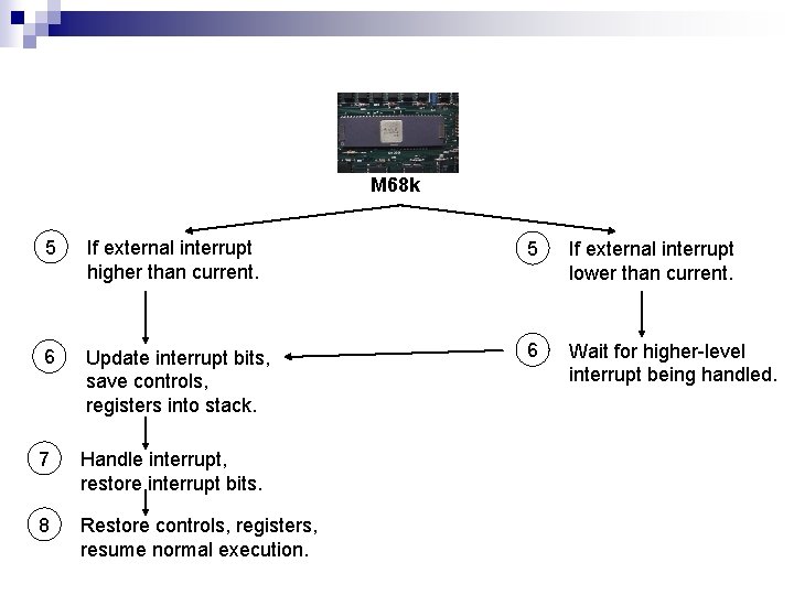
M 68 k 5 If external interrupt higher than current. 5 If external interrupt lower than current. 6 Update interrupt bits, save controls, registers into stack. 6 Wait for higher-level interrupt being handled. 7 Handle interrupt, restore interrupt bits. 8 Restore controls, registers, resume normal execution.

Bus Arbitration Control

+5 V VCC D 0 -D 15 Data Bus A 1 -A 23 Address Bus CLK *A 0 is used inside 68 k AS Processor Status FC 0 R/W FC 1 UDS FC 2 68000 DTACK E 6800 Peripheral Control VMA BR VPA BG BERR System Control LDS Asynchronous Bus Control Bus Arbitration Control BGACK RESET IPL 0 HALT IPL 1 GND IPL 2 Interrupt Control

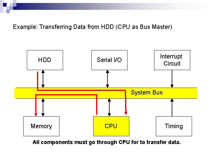
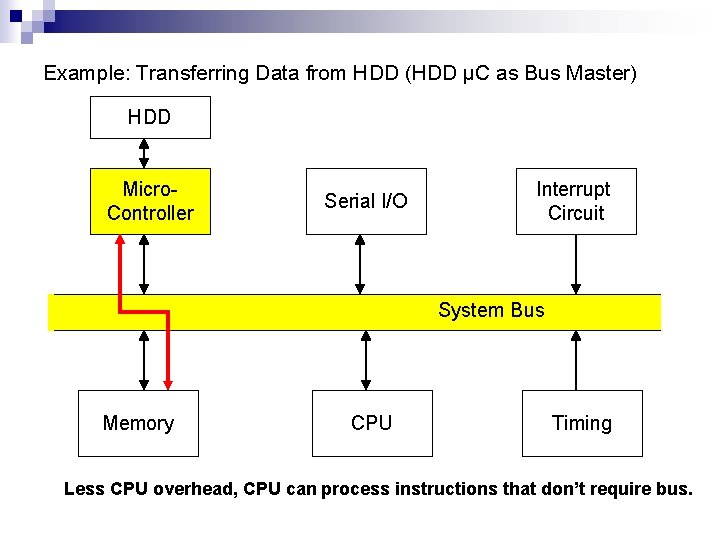
Bus Arbitration Control n Carries signals that allow bus takeovers: ¨ M 68 k releases bus control to external device. ¨ Faster data transfer, multi-CPU architecture, less overhead. ¨ M 68 k waits, then takes back bus control. n Lets external devices become bus masters: Device must have own microcontroller. n Accesses other peripherals as if it was CPU. n Usually for DMA. n

Example: Transferring Data from HDD (CPU as Bus Master) HDD Serial I/O Interrupt Circuit System Bus Memory CPU Timing All components must go through CPU for to transfer data.

Example: Transferring Data from HDD (HDD µC as Bus Master) HDD Micro. Controller Serial I/O Interrupt Circuit System Bus Memory CPU Timing Less CPU overhead, CPU can process instructions that don’t require bus.

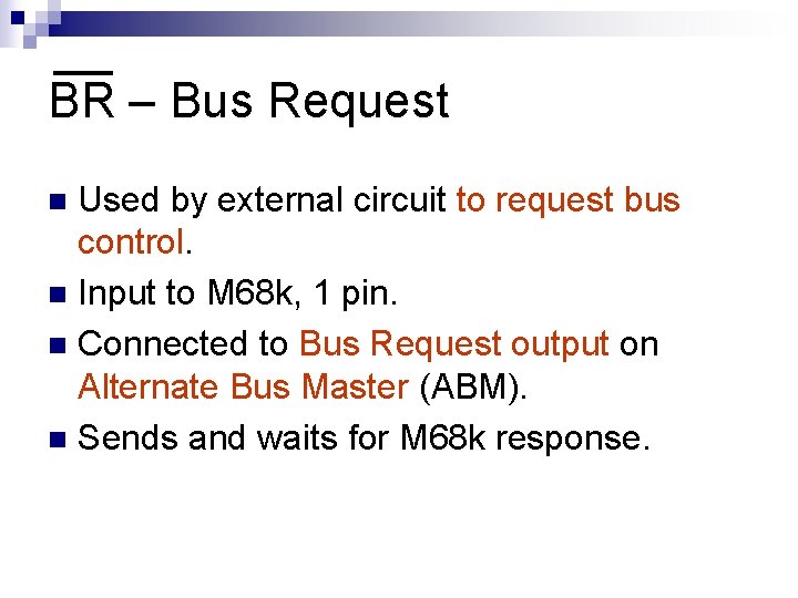
BR – Bus Request Used by external circuit to request bus control. n Input to M 68 k, 1 pin. n Connected to Bus Request output on Alternate Bus Master (ABM). n Sends and waits for M 68 k response. n

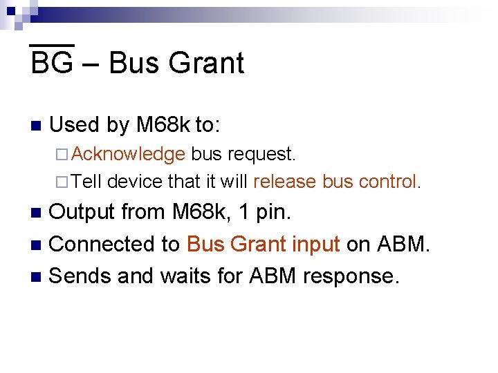
BG – Bus Grant n Used by M 68 k to: ¨ Acknowledge bus request. ¨ Tell device that it will release bus control. Output from M 68 k, 1 pin. n Connected to Bus Grant input on ABM. n Sends and waits for ABM response. n

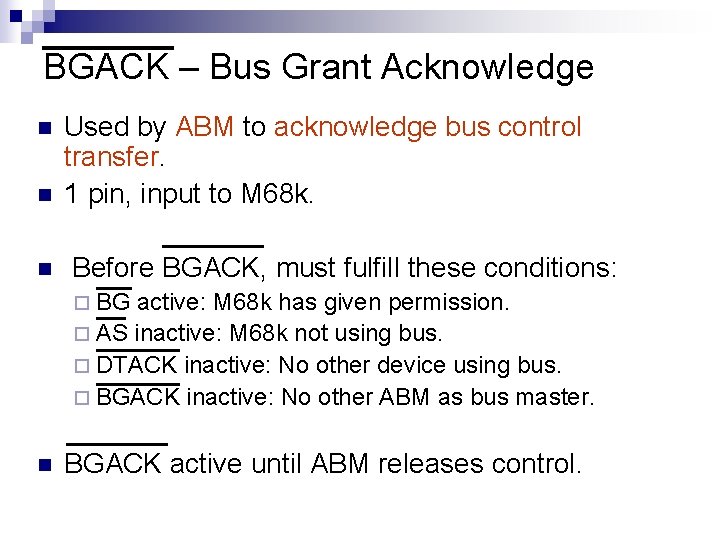
BGACK – Bus Grant Acknowledge n n n Used by ABM to acknowledge bus control transfer. 1 pin, input to M 68 k. Before BGACK, must fulfill these conditions: ¨ BG active: M 68 k has given permission. ¨ AS inactive: M 68 k not using bus. ¨ DTACK inactive: No other device using bus. ¨ BGACK inactive: No other ABM as bus master. n BGACK active until ABM releases control.

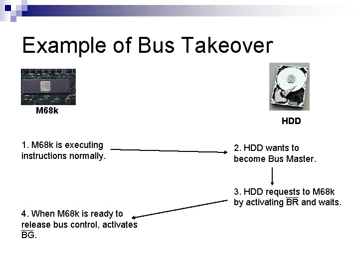
Example of Bus Takeover M 68 k HDD 1. M 68 k is executing instructions normally. 2. HDD wants to become Bus Master. 3. HDD requests to M 68 k by activating BR and waits. 4. When M 68 k is ready to release bus control, activates BG.

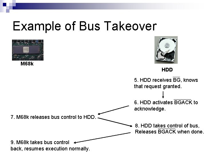
Example of Bus Takeover M 68 k HDD 5. HDD receives BG, knows that request granted. 6. HDD activates BGACK to acknowledge. 7. M 68 k releases bus control to HDD. 8. HDD takes control of bus, Releases BGACK when done. 9. M 68 k takes bus control back, resumes execution normally.

Data & Address Bus

+5 V VCC D 0 -D 15 Data Bus A 1 -A 23 Address Bus CLK *A 0 is used inside 68 k AS Processor Status FC 0 R/W FC 1 UDS FC 2 68000 DTACK E 6800 Peripheral Control VMA BR VPA BG BERR System Control LDS Asynchronous Bus Control Bus Arbitration Control BGACK RESET IPL 0 HALT IPL 1 GND IPL 2 Interrupt Control

Data Bus Used for general-purpose data transfer. n 16 -bits (D 0 to D 15), bi-directional. n Can transfer word or byte data. n Also used to carry vector number during Interrupt Acknowledge Cycle. n

Address Bus Used to carry address values. n 23 -bits (A 1 – A 23), one-directional. n A 0 used internally, spurs UDS, LDS. n Able to address 16 MB of memory. n

Asynchronous Bus Control

+5 V VCC D 0 -D 15 Data Bus A 1 -A 23 Address Bus CLK *A 0 is used inside 68 k AS Processor Status FC 0 R/W FC 1 UDS FC 2 68000 DTACK E 6800 Peripheral Control VMA BR VPA BG BERR System Control LDS Asynchronous Bus Control Bus Arbitration Control BGACK RESET IPL 0 HALT IPL 1 GND IPL 2 Interrupt Control

Asynchronous Bus Control Group Responsible for asynchronous data transfer. n Most common data transfer method. n 5 pins: n ¨ Regulate data transfer: AS, DTACK. ¨ Activate device: UDS, LDS. ¨ Type of operation: R/W.

Asynchronous Transfer n Used to perform asynchronous data transfer: ¨ Doesn’t follow strict timing from CLK. ¨ Transfer based on “handshaking” between sender and receiver: CLK replaced by sender-ready and receiver-ready. n Sender sends data when its ready. n Receiver sends signal when transfer completes. n

AS – Address Strobe n Purpose: ¨ Indicates M 68 k using bus. ¨ Valid address on address bus. n Activated when M 68 k wants to use bus: ¨ Begin reading from memory. ¨ Begin writing to memory. ¨ Access peripherals.

R/W Used to specify read/write operation. n 1 pin, output. n Three states: n ¨ High (1): read (default). ¨ Low (0): write. ¨ High-impedance: when ABS is controlling bus.

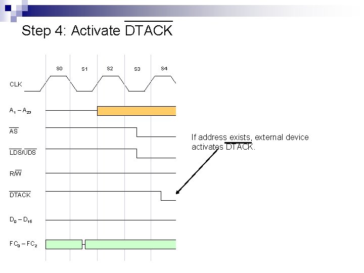
DTACK – Data Transfer Acknowledge n n Indicates device ready to begin data transfer. Generated by external device being accessed. When M 68 k receives signal, knows data transfer can be started, begins read/write. During data transfer, M 68 k inserts wait states until DTACK is received.

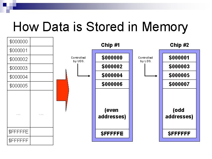
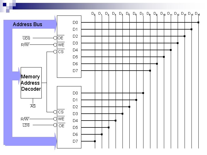
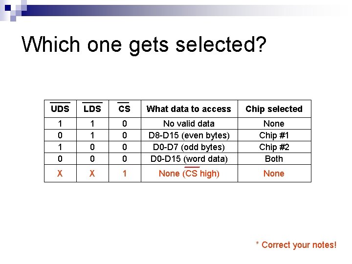
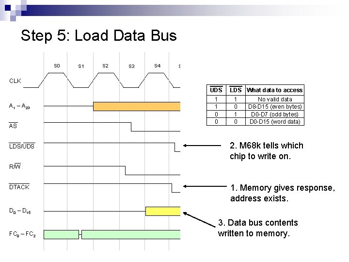
UDS/LDS n Used to activate correct memory chip during read/write: ¨ Data usually stored in pairs of chips. ¨ Each chip partially connected to data bus. ¨ LDS activates D 0 to D 7 (odd bytes). ¨ UDS activates D 8 to D 15 (even bytes).

How Data is Stored in Memory $000000 Chip #1 $000001 Controlled by UDS. $000002 $000000 Chip #2 Controlled by LDS. $000001 $000003 $000002 $000003 $000004 $000005 $000006 $000007 (even addresses) (odd addresses) $FFFFFE $FFFFFF …

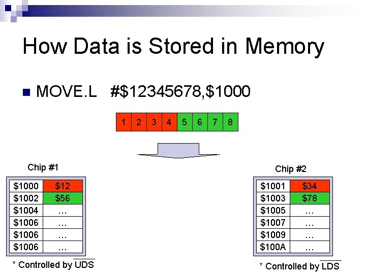
How Data is Stored in Memory n MOVE. L #$12345678, $1000 1 Chip #1 $1000 $1002 $1004 $1006 $12 $56 … … * Controlled by UDS 2 3 4 5 6 7 8 Chip #2 $1001 $1003 $1005 $1007 $1009 $100 A $34 $78 … … * Controlled by LDS

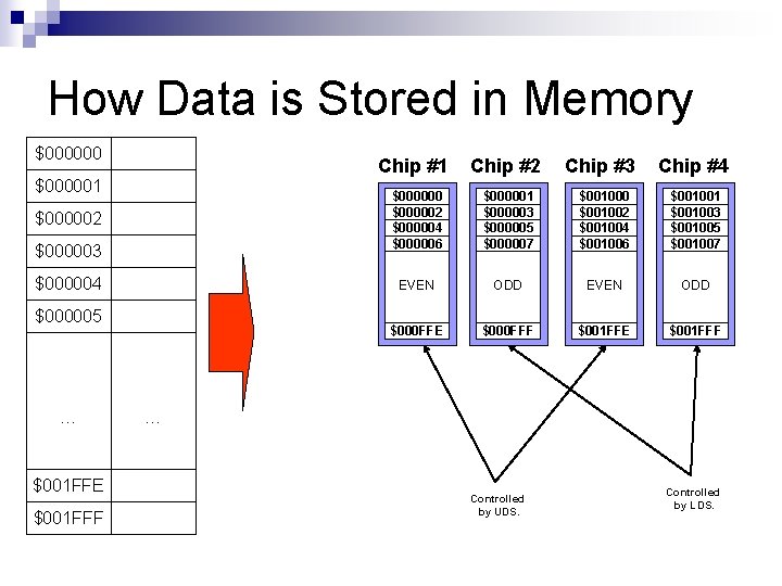
How Data is Stored in Memory $000000 Chip #1 $000002 $000003 $000004 $000005 … $001 FFE $001 FFF Chip #2 Chip #3 Chip #4 $000000 $000002 $000004 $000006 $000001 $000003 $000005 $000007 $001000 $001002 $001004 $001006 $001001 $001003 $001005 $001007 EVEN ODD $000 FFE $000 FFF $001 FFE $001 FFF … Controlled by UDS. Controlled by LDS.

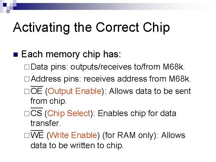
Activating the Correct Chip n Each memory chip has: ¨ Data pins: outputs/receives to/from M 68 k. ¨ Address pins: receives address from M 68 k. ¨ OE (Output Enable): Allows data to be sent from chip. ¨ CS (Chip Select): Enables chip for data transfer. ¨ WE (Write Enable) (for RAM only): Allows data to be written to chip.

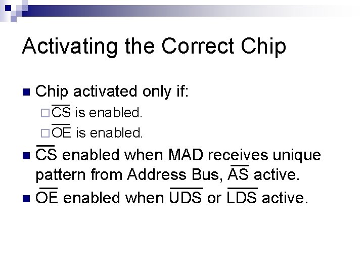
Activating the Correct Chip n Chip activated only if: ¨ CS is enabled. ¨ OE is enabled. CS enabled when MAD receives unique pattern from Address Bus, AS active. n OE enabled when UDS or LDS active. n

D 0 D 1 D 2 D 3 D 4 D 5 D 6 D 7 D 8 D 9 D 10 D 11 D 12 D 13 D 14 D 15 D 0 Address Bus D 1 UDS R/W OE D 2 WE D 3 CS D 4 D 5 D 6 D 7 Memory Address Decoder D 0 D 1 AS D 2 CS D 3 R/W WE D 4 LDS OE D 5 D 6 D 7

Which one gets selected? UDS LDS CS What data to access Chip selected 1 0 1 1 0 0 0 No valid data D 8 -D 15 (even bytes) D 0 -D 7 (odd bytes) D 0 -D 15 (word data) None Chip #1 Chip #2 Both X X 1 None (CS high) None * Correct your notes!

Read Cycle

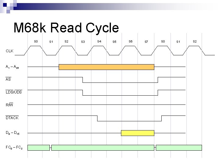
M 68 k Read Cycle S 0 CLK A 1 – A 23 AS LDS/UDS R/W DTACK D 0 – D 15 FC 0 – FC 2 S 1 S 2 S 3 S 4 S 5 S 6 S 7 S 0 S 1 S 2

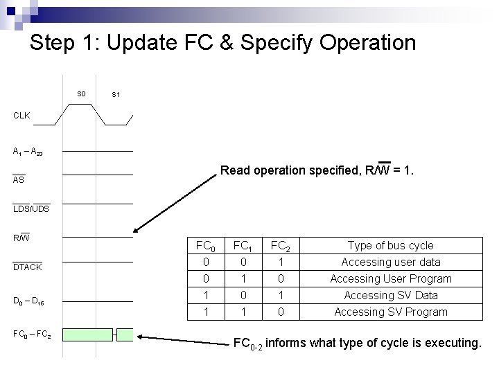
Step 1: Update FC & Specify Operation S 0 S 1 S 2 S 4 S 3 S 6 S 5 S 7 S 0 S 1 S 2 CLK A 1 – A 23 Read operation specified, R/W = 1. AS LDS/UDS R/W DTACK D 0 – D 15 FC 0 – FC 2 FC 0 0 0 1 1 FC 1 0 1 FC 2 1 0 Type of bus cycle Accessing user data Accessing User Program Accessing SV Data Accessing SV Program FC 0 -2 informs what type of cycle is executing.

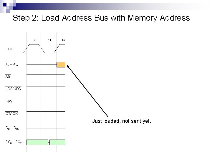
Step 2: Load Address Bus with Memory Address S 0 S 1 S 2 S 3 S 4 S 5 S 6 S 7 CLK A 1 – A 23 AS LDS/UDS R/W DTACK Just loaded, not sent yet. D 0 – D 15 FC 0 – FC 2 S 0 S 1 S 2

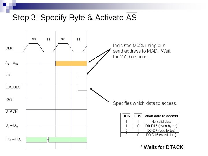
Step 3: Specify Byte & Activate AS S 0 CLK S 1 S 2 S 3 S 4 S 5 S 6 S 7 S 0 S 1 S 2 Indicates M 68 k using bus, send address to MAD. Wait for MAD response. A 1 – A 23 AS LDS/UDS R/W Specifies which data to access. DTACK UDS D 0 – D 15 1 1 0 0 LDS What data to access 1 0 No valid data D 8 -D 15 (even bytes) D 0 -D 7 (odd bytes) D 0 -D 15 (word data) FC 0 – FC 2 * Waits for DTACK

Step 4: Activate DTACK S 0 S 1 S 2 S 3 S 4 S 5 S 6 S 7 S 0 S 1 CLK A 1 – A 23 AS LDS/UDS R/W DTACK D 0 – D 15 FC 0 – FC 2 If address exists, external device activates DTACK. S 2

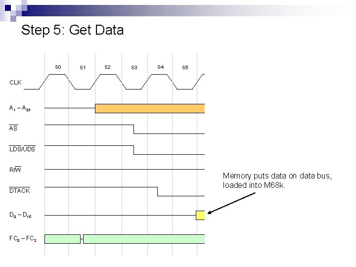
Step 5: Get Data S 0 S 1 S 2 S 3 S 4 S 5 S 6 S 7 S 0 S 1 S 2 CLK A 1 – A 23 AS LDS/UDS R/W DTACK D 0 – D 15 FC 0 – FC 2 Memory puts data on data bus, loaded into M 68 k.

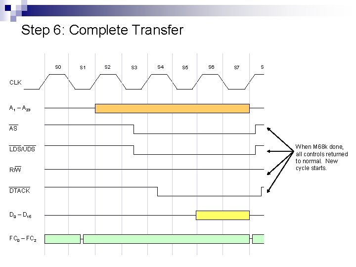
Step 6: Complete Transfer S 0 S 1 S 2 S 3 S 4 S 5 S 6 S 7 S 0 S 1 S 2 CLK A 1 – A 23 AS LDS/UDS R/W DTACK D 0 – D 15 FC 0 – FC 2 When M 68 k done, all controls returned to normal. New cycle starts.

Write Cycle

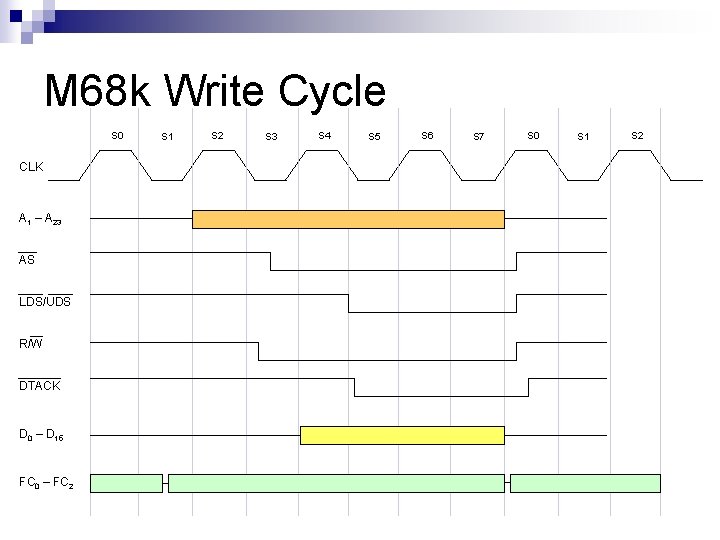
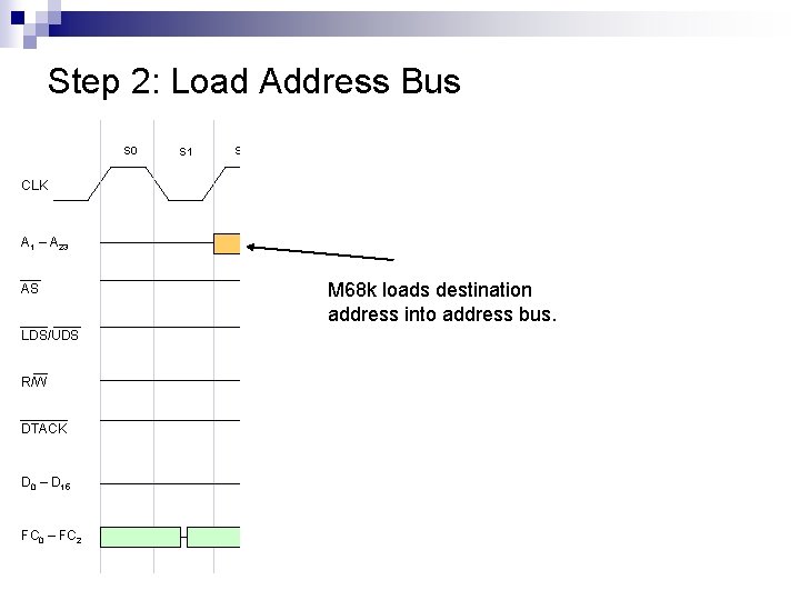
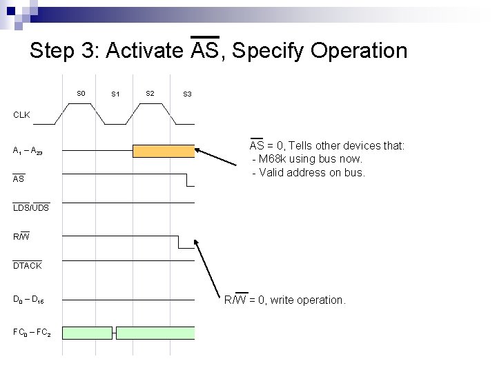
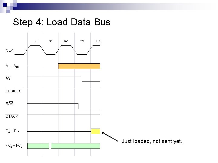
M 68 k Write Cycle S 0 CLK A 1 – A 23 AS LDS/UDS R/W DTACK D 0 – D 15 FC 0 – FC 2 S 1 S 2 S 3 S 4 S 5 S 6 S 7 S 0 S 1 S 2

Step 1: Specify Operation S 0 S 1 S 2 S 4 S 3 S 6 S 5 S 7 S 0 S 1 S 2 CLK A 1 – A 23 AS LDS/UDS R/W DTACK D 0 – D 15 FC 0 – FC 2 FC 0 0 0 1 1 FC 1 0 1 FC 2 1 0 Type of bus cycle Accessing user data Accessing User Program Accessing SV Data Accessing SV Program FC 0 -2 informs what type of cycle is executing.

Step 2: Load Address Bus S 0 S 1 S 2 S 3 S 4 S 5 S 6 S 7 CLK A 1 – A 23 AS LDS/UDS R/W DTACK D 0 – D 15 FC 0 – FC 2 M 68 k loads destination address into address bus. S 0 S 1 S 2

Step 3: Activate AS, Specify Operation S 0 S 1 S 2 S 3 S 4 S 5 S 6 S 7 S 0 S 1 CLK A 1 – A 23 AS AS = 0, Tells other devices that: - M 68 k using bus now. - Valid address on bus. LDS/UDS R/W DTACK D 0 – D 15 FC 0 – FC 2 R/W = 0, write operation. S 2

Step 4: Load Data Bus S 0 S 1 S 2 S 3 S 4 S 5 S 6 S 7 S 0 S 1 CLK A 1 – A 23 AS LDS/UDS R/W DTACK D 0 – D 15 FC 0 – FC 2 Just loaded, not sent yet. S 2

Step 5: Load Data Bus S 0 S 1 S 2 S 3 S 4 S 5 S 6 S 7 S 0 S 1 S 2 CLK UDS A 1 – A 23 AS LDS/UDS 1 1 0 0 LDS What data to access 1 0 No valid data D 8 -D 15 (even bytes) D 0 -D 7 (odd bytes) D 0 -D 15 (word data) 2. M 68 k tells which chip to write on. R/W DTACK 1. Memory gives response, address exists. D 0 – D 15 FC 0 – FC 2 3. Data bus contents written to memory.

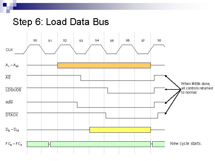
Step 6: Load Data Bus S 0 S 1 S 2 S 3 S 4 S 5 S 6 S 7 S 0 S 1 S 2 CLK A 1 – A 23 AS LDS/UDS When M 68 k done, all controls returned to normal. R/W DTACK D 0 – D 15 FC 0 – FC 2 New cycle starts.

Conclusion

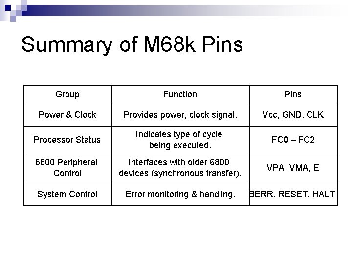
Summary of M 68 k Pins Group Function Pins Power & Clock Provides power, clock signal. Vcc, GND, CLK Processor Status Indicates type of cycle being executed. FC 0 – FC 2 6800 Peripheral Control Interfaces with older 6800 devices (synchronous transfer). VPA, VMA, E System Control Error monitoring & handling. BERR, RESET, HALT

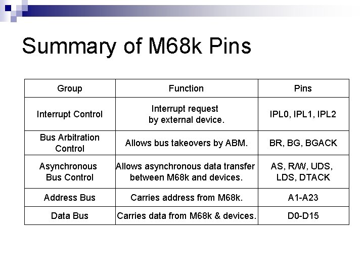
Summary of M 68 k Pins Group Function Pins Interrupt Control Interrupt request by external device. IPL 0, IPL 1, IPL 2 Bus Arbitration Control Allows bus takeovers by ABM. BR, BGACK Asynchronous Bus Control Allows asynchronous data transfer between M 68 k and devices. AS, R/W, UDS, LDS, DTACK Address Bus Carries address from M 68 k. A 1 -A 23 Data Bus Carries data from M 68 k & devices. D 0 -D 15

The End Please read: Antonakos, pg. 238 -254