ECE 511 Digital System Microprocessor Course Outline Week





- Slides: 63

ECE 511: Digital System & Microprocessor

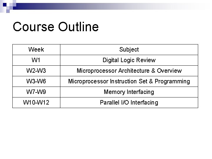
Course Outline Week Subject W 1 Digital Logic Review W 2 -W 3 Microprocessor Architecture & Overview W 3 -W 6 Microprocessor Instruction Set & Programming W 7 -W 9 Memory Interfacing W 10 -W 12 Parallel I/O Interfacing

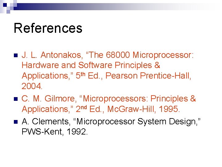
References n n n J. L. Antonakos, “The 68000 Microprocessor: Hardware and Software Principles & Applications, ” 5 th Ed. , Pearson Prentice-Hall, 2004. C. M. Gilmore, “Microprocessors: Principles & Applications, ” 2 nd Ed. , Mc. Graw-Hill, 1995. A. Clements, “Microprocessor System Design, ” PWS-Kent, 1992.

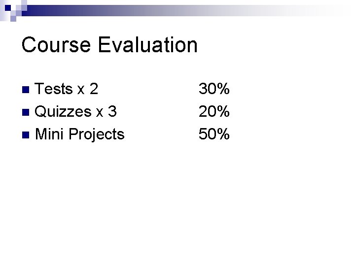
Course Evaluation Tests x 2 n Quizzes x 3 n Mini Projects n 30% 20% 50%

If you have problems, please contact me: Ahmad Ihsan bin Mohd Yassin Rm. T 2 -A 13 -1 A, Dept. of Comp. Eng. Faculty of Elect. Eng. Ui. TM, Shah Alam. 03 -55436118, 017 -2576295 *Please call before you see me.

Digital Logic Review: Part I ECE 511: Digital System & Microprocessor.

What we will learn in this session: Review of logic gates. n Flip-flops. n Decoders. n Universal representation of logic gates. n

Gates

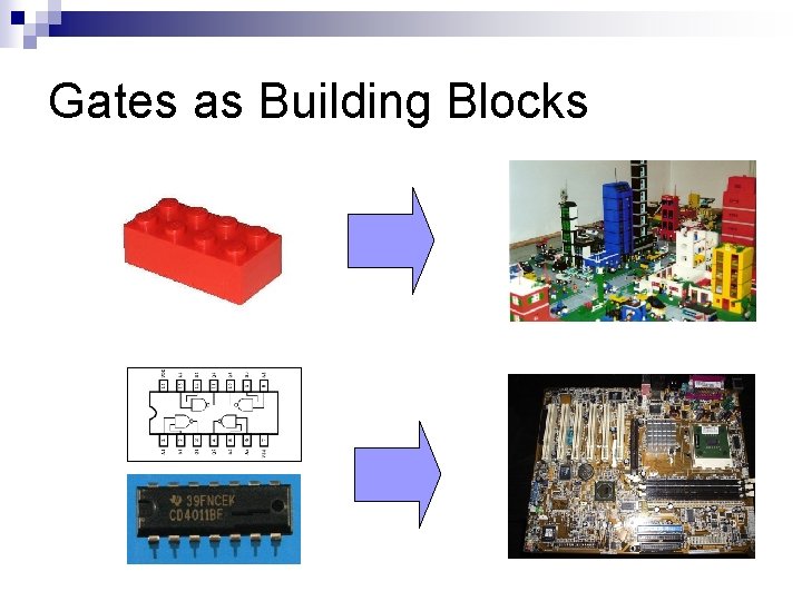
What are gates? n Gates are: ¨ Simple electronic devices. ¨ Constructed using transistors. ¨ Used to design digital systems. n Three Basic Gates: ¨ AND ¨ OR ¨ NOT n n Basic Gates can be combined into Extended Gates. Usually packed into ICs.

Gates as Building Blocks

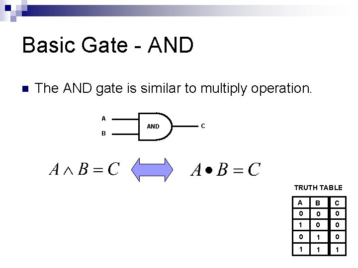
Basic Gate - AND n The AND gate is similar to multiply operation. A AND C B TRUTH TABLE A B C 0 0 0 1 0 1 1 1

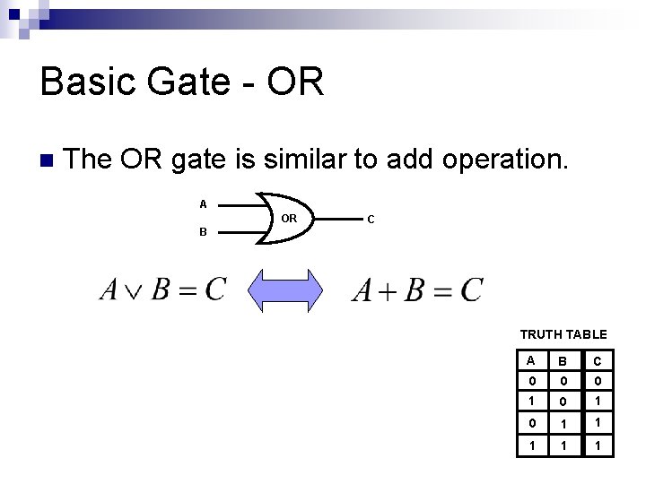
Basic Gate - OR n The OR gate is similar to add operation. A OR B C TRUTH TABLE A B C 0 0 0 1 0 1 1 1

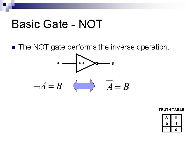
Basic Gate - NOT n The NOT gate performs the inverse operation. A NOT B TRUTH TABLE A B 0 1 1 0

Extended Gates n Combination of basic gates to perform complex functions: ¨ NAND ¨ NOR ¨ XNOR ¨ Flip-Flops

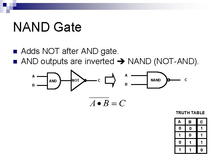
NAND Gate n n Adds NOT after AND gate. AND outputs are inverted NAND (NOT-AND). A A AND B NOT C NAND C B TRUTH TABLE A B C 0 0 1 1 0

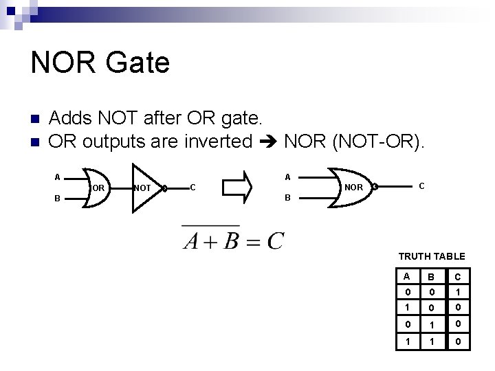
NOR Gate n n Adds NOT after OR gate. OR outputs are inverted NOR (NOT-OR). A A OR B NOT C NOR C B TRUTH TABLE A B C 0 0 1 1 0

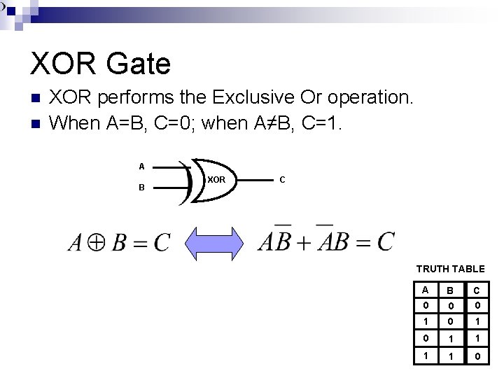
XOR Gate n n XOR performs the Exclusive Or operation. When A=B, C=0; when A≠B, C=1. A B XOR C TRUTH TABLE A B C 0 0 0 1 0 1 1 0

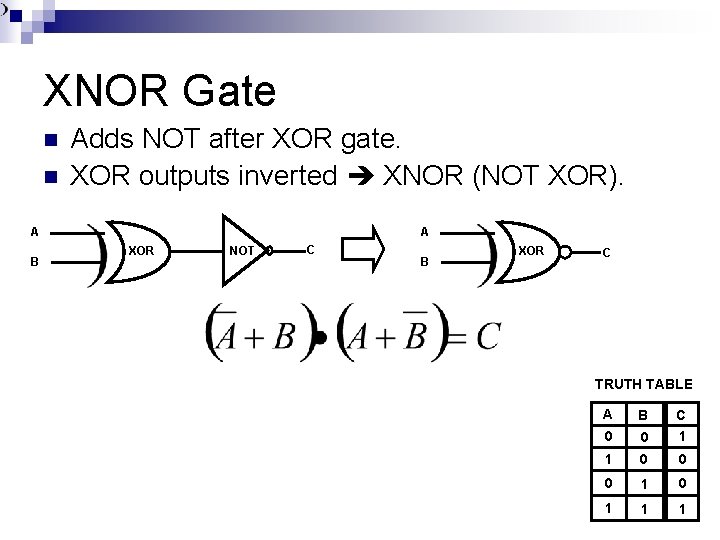
XNOR Gate n n Adds NOT after XOR gate. XOR outputs inverted XNOR (NOT XOR). A A B XOR NOT C B XOR C TRUTH TABLE A B C 0 0 1 1 0 0 0 1 1 1

Flip-Flops

Flip-Flops n An extended gate used as memory: ¨ Each FF stores 1 bit. 2 gates, feedback connections. n 2 inputs, 2 outputs. n More complex ones may: n ¨ Use timing from CLK. ¨ Perform bit toggle.

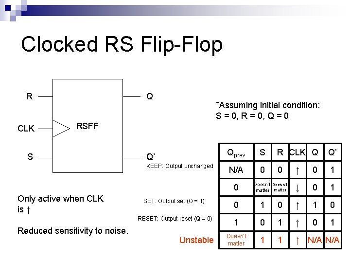
Reset-Set (RS) Flip-Flop n 4 states: ¨ Three stable (Set, Reset, and Keep). ¨ One not stable (Unused). n n 2 inputs, 2 outputs. May also contain clock (CLK) signal.

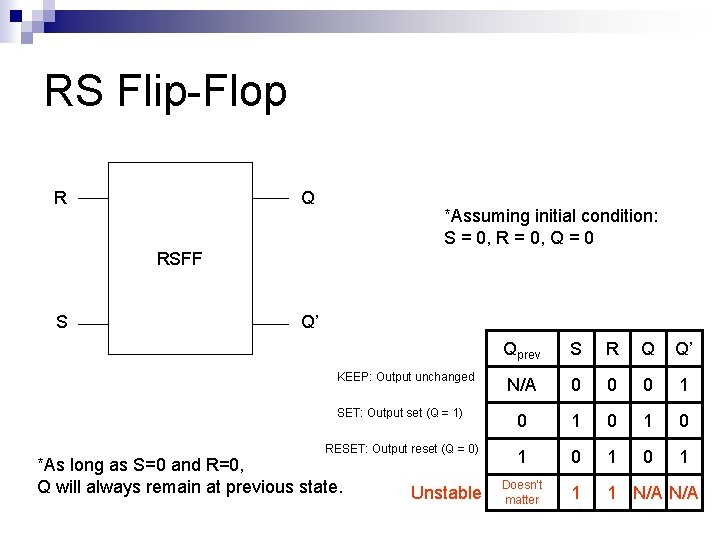
RS Flip-Flop R Q *Assuming initial condition: S = 0, R = 0, Q = 0 RSFF S Q’ Qprev S R Q Q’ N/A 0 0 0 1 SET: Output set (Q = 1) 0 1 0 RESET: Output reset (Q = 0) 1 0 1 Doesn’t matter 1 1 N/A KEEP: Output unchanged *As long as S=0 and R=0, Q will always remain at previous state. Unstable

Clocked RS Flip-Flop R CLK Q *Assuming initial condition: S = 0, R = 0, Q = 0 RSFF S Q’ KEEP: Output unchanged Qprev S R CLK Q Q’ N/A 0 0 0 Only active when CLK is ↑ Reduced sensitivity to noise. Doesn’t matter ↑ 0 1 ↓ 0 1 SET: Output set (Q = 1) 0 1 0 ↑ 1 0 RESET: Output reset (Q = 0) 1 0 1 ↑ 0 1 Doesn’t matter 1 1 ↑ N/A Unstable

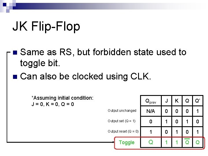
JK Flip-Flop Same as RS, but forbidden state used to toggle bit. n Can also be clocked using CLK. n *Assuming initial condition: J = 0, K = 0, Q = 0 Qprev J K Q Q’ Output unchanged N/A 0 0 0 1 Output set (Q = 1) 0 1 0 Output reset (Q = 0) 1 0 1 Q 1 1 Q Q Toggle

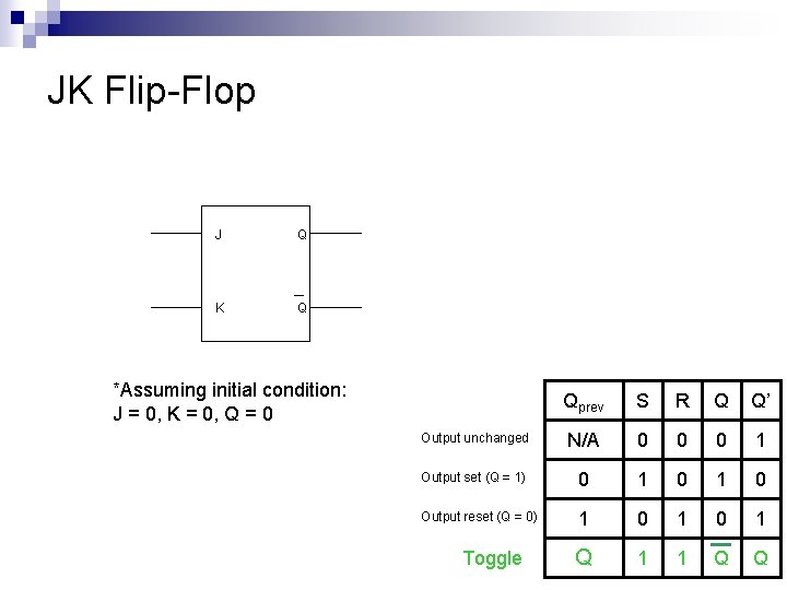
JK Flip-Flop J Q K Q *Assuming initial condition: J = 0, K = 0, Q = 0 Qprev S R Q Q’ Output unchanged N/A 0 0 0 1 Output set (Q = 1) 0 1 0 Output reset (Q = 0) 1 0 1 Q 1 1 Q Q Toggle

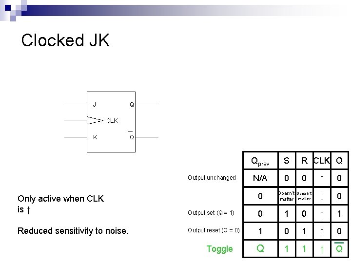
Clocked JK J Q CLK K Q Output unchanged Qprev S R CLK Q N/A 0 0 0 Doesn’t matter ↑ 0 ↓ 0 Only active when CLK is ↑ Output set (Q = 1) 0 1 0 ↑ 1 Reduced sensitivity to noise. Output reset (Q = 0) 1 0 1 ↑ 0 Q 1 1 ↑ Q Toggle

D-Flip-Flop Data latch. n Modification of RSFF. n Stores 1 -bit of information. n ¨ Can n be combined to store more. Data are stored in memory using millions of DFFs.

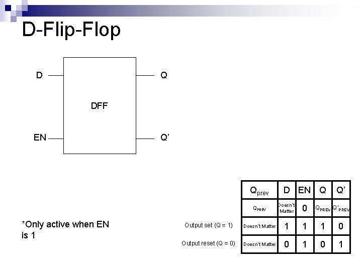
D-Flip-Flop D Q DFF EN Q’ Qprev *Only active when EN is 1 D EN Q Q’ QPREV Doesn’t Matter 0 Output set (Q = 1) Doesn’t Matter 1 1 1 0 Output reset (Q = 0) Doesn’t Matter 0 1 QPREV Q’PREV

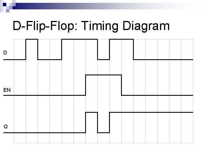
D-Flip-Flop: Timing Diagram D EN Q

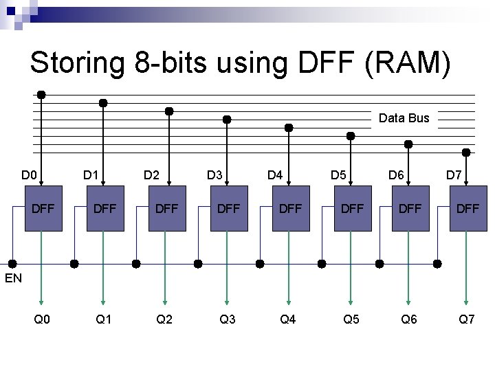
Storing 8 -bits using DFF (RAM) Data Bus D 0 D 1 D 2 D 3 D 4 D 5 D 6 D 7 DFF DFF Q 0 Q 1 Q 2 Q 3 Q 4 Q 5 Q 6 Q 7 EN

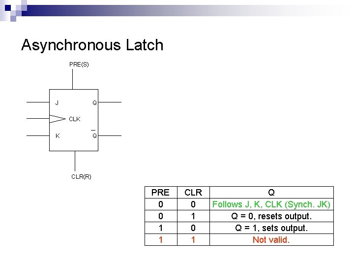
Asynchronous Latch n Allows both synchronous & asynchronous operations: ¨ Synchronous: CLK driven (Clocked JK). ¨ Asynchronous: similar to RSFF. n 5 inputs, 2 outputs: ¨ J, K and CLK for synch. operation. ¨ PR, CLR for asynch. operation.

Asynchronous Latch PRE(S) J Q CLK K Q CLR(R) PRE 0 0 1 1 CLR 0 1 Q Follows J, K, CLK (Synch. JK) Q = 0, resets output. Q = 1, sets output. Not valid.

Universal Gates – NAND and NOR

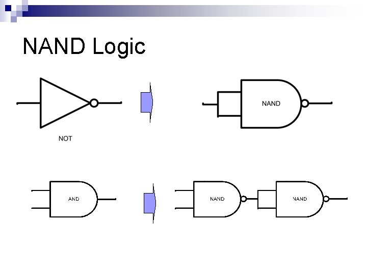
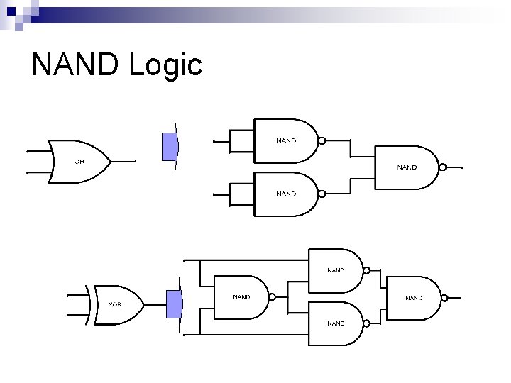
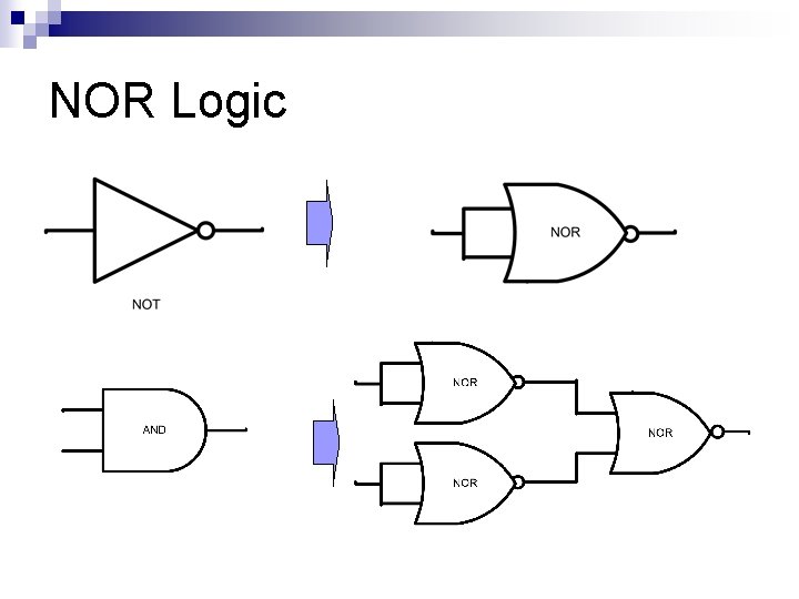
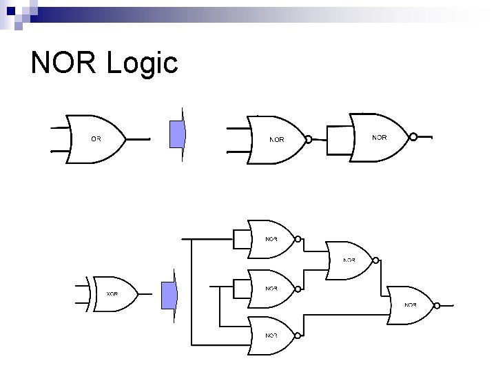
NAND and NOR as Universal Gates In industry, NAND and NOR gates are most common. n Reason? n ¨ Can be used to represent any gate (functionally complete). ¨ Easiest & cheapest to produce.

NAND Logic

NAND Logic

NOR Logic

NOR Logic

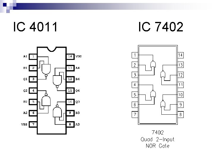
IC 4011 IC 7402

Decoders

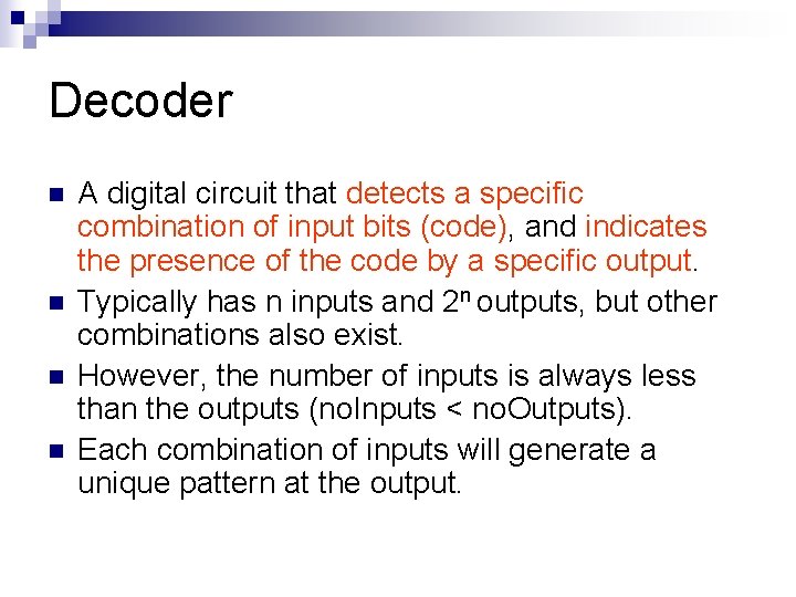
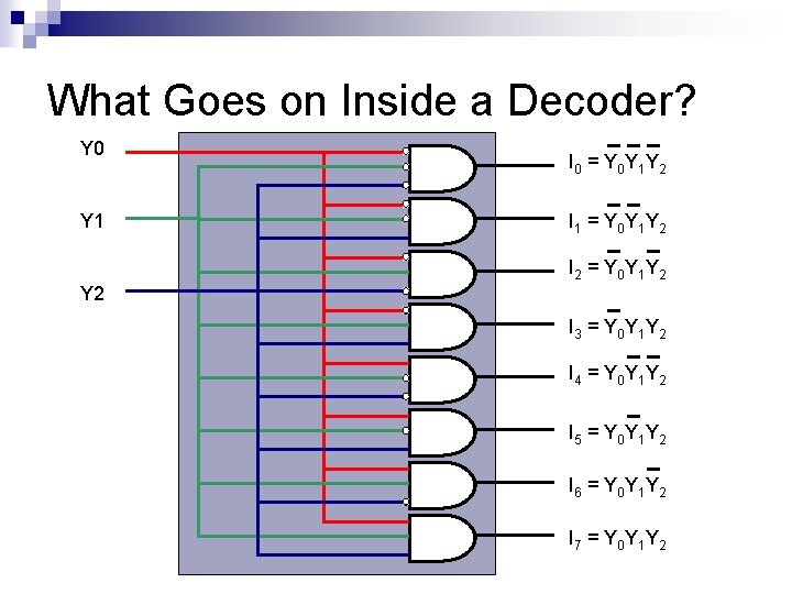
Decoder n n A digital circuit that detects a specific combination of input bits (code), and indicates the presence of the code by a specific output. Typically has n inputs and 2 n outputs, but other combinations also exist. However, the number of inputs is always less than the outputs (no. Inputs < no. Outputs). Each combination of inputs will generate a unique pattern at the output.

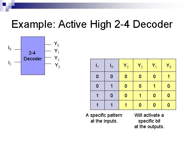
Example: Active High 2 -4 Decoder I 0 I 1 Y 0 2 -4 Decoder Y 1 Y 2 Y 3 I 1 I 0 Y 3 Y 2 Y 1 Y 0 0 0 1 0 1 0 0 1 1 1 0 0 0 A specific pattern at the inputs. Will activate a specific bit at the outputs.

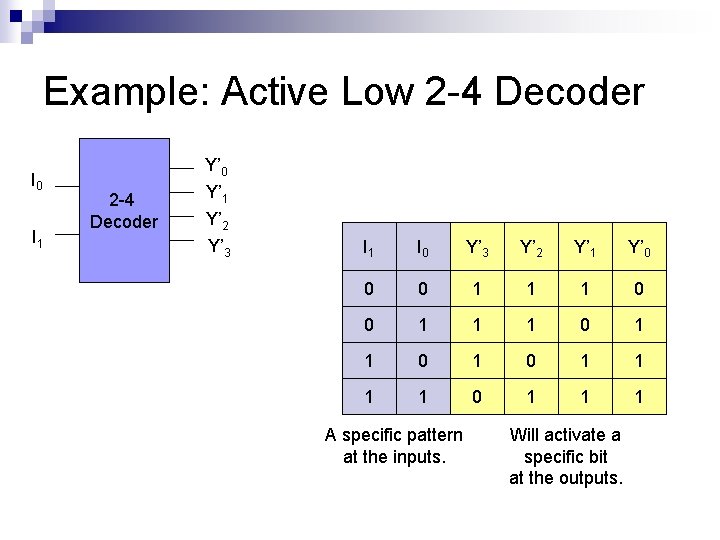
Example: Active Low 2 -4 Decoder I 0 I 1 Y’ 0 2 -4 Decoder Y’ 1 Y’ 2 Y’ 3 I 1 I 0 Y’ 3 Y’ 2 Y’ 1 Y’ 0 0 0 1 1 1 0 1 1 0 1 1 1 A specific pattern at the inputs. Will activate a specific bit at the outputs.

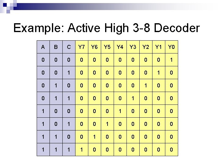
Example: Active High 3 -8 Decoder A B C Y 7 Y 6 Y 5 Y 4 Y 3 Y 2 Y 1 Y 0 0 0 1 0 0 0 0 0 0 1 1 0 0 0 0 0 1 0 0 1 0 0 0 1 1 0 0 0 0

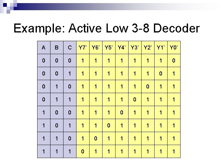
Example: Active Low 3 -8 Decoder A B C Y 7’ Y 6’ Y 5’ Y 4’ Y 3’ Y 2’ Y 1’ Y 0’ 0 0 0 1 1 1 1 0 1 0 1 1 1 1 0 0 1 1 1 1 1 1 1 0 1 1 1 1

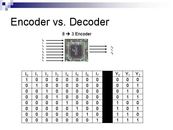
Encoder vs. Decoder 8 3 Encoder I 0 I 1 I 2 I 3 I 4 I 5 I 6 I 7 I 0 1 0 0 0 0 I 1 0 0 0 0 Y 2 Y 1 Y 0 I 2 0 0 1 0 0 0 I 3 0 0 0 1 0 0 I 4 0 0 1 0 0 0 I 5 0 0 0 1 0 0 I 6 0 0 0 1 0 I 7 0 0 0 0 1 Y 0 0 0 1 1 Y 1 0 0 1 1 Y 2 0 1 0 1

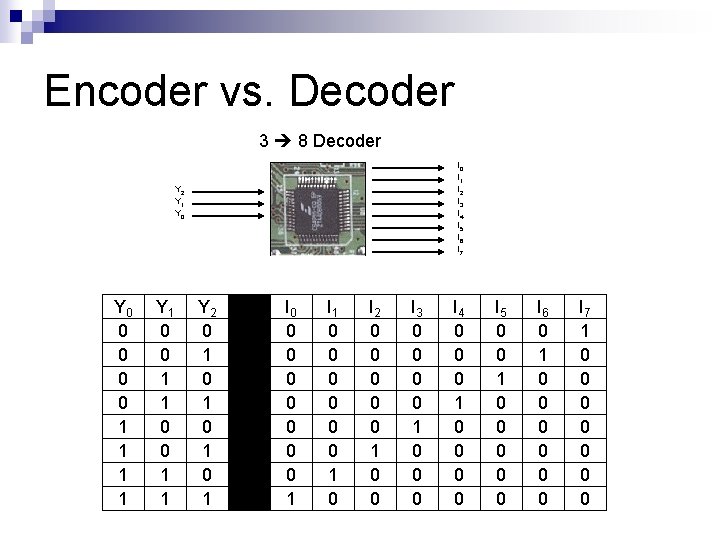
Encoder vs. Decoder 3 8 Decoder I 0 I 1 I 2 I 3 I 4 I 5 I 6 I 7 Y 2 Y 1 Y 0 0 0 1 1 Y 1 0 0 1 1 Y 2 0 1 0 1 I 0 0 0 0 1 I 1 0 0 0 1 0 I 2 0 0 0 1 0 0 I 3 0 0 1 0 0 0 I 4 0 0 0 1 0 0 I 5 0 0 1 0 0 0 I 6 0 1 0 0 0 I 7 1 0 0 0 0

What Goes on Inside a Decoder? Y 0 Y 1 I 0 = Y 0 Y 1 Y 2 I 1 = Y 0 Y 1 Y 2 I 2 = Y 0 Y 1 Y 2 I 3 = Y 0 Y 1 Y 2 I 4 = Y 0 Y 1 Y 2 I 5 = Y 0 Y 1 Y 2 I 6 = Y 0 Y 1 Y 2 I 7 = Y 0 Y 1 Y 2

Decoders n In this subject, you need to familiarize yourself with two types of decoders: ¨ 74 LS 139 Dual 2 -4 Line Decoder. ¨ 74 LS 138 3 -8 Line Decoder n Decoders are used to: ¨ Activate devices for use by µP. ¨ Memory, I/O interfacing.

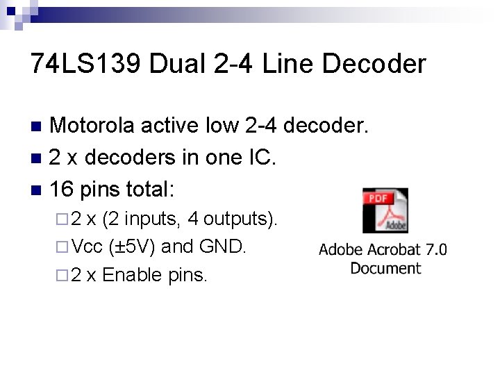
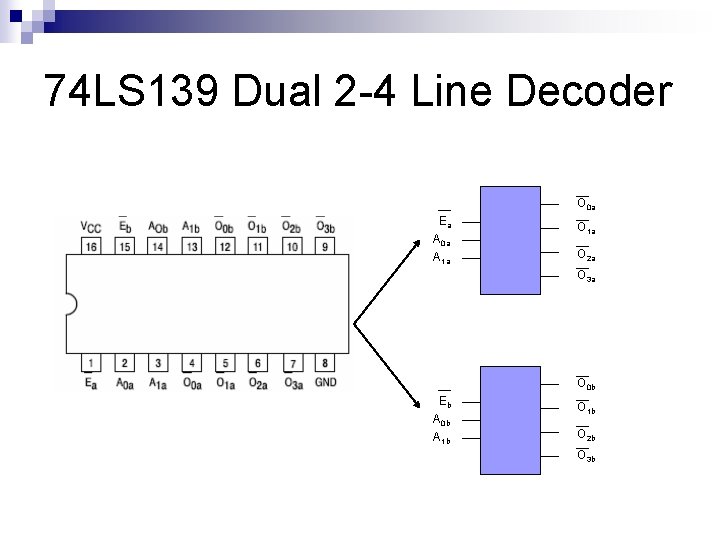
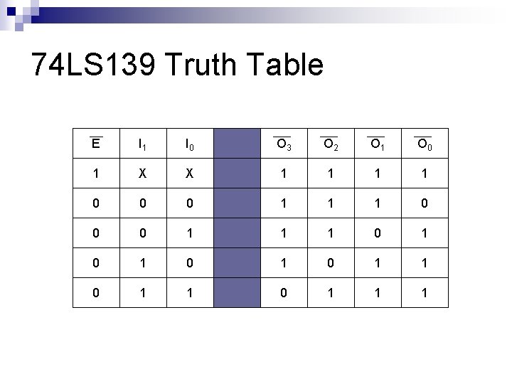
74 LS 139 Dual 2 -4 Line Decoder Motorola active low 2 -4 decoder. n 2 x decoders in one IC. n 16 pins total: n ¨ 2 x (2 inputs, 4 outputs). ¨ Vcc (± 5 V) and GND. ¨ 2 x Enable pins.

74 LS 139 Dual 2 -4 Line Decoder O 0 a Ea A 0 a A 1 a O 2 a O 3 a O 0 b Eb A 0 b A 1 b O 2 b O 3 b

74 LS 139 Truth Table E I 1 I 0 O 3 O 2 O 1 O 0 1 X X 1 1 0 0 0 1 1 1 0 1 0 1 1 1

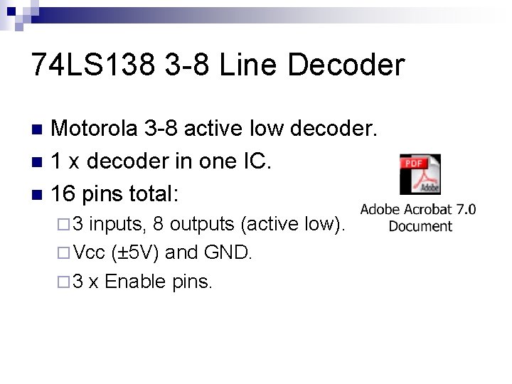
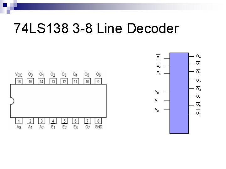
74 LS 138 3 -8 Line Decoder Motorola 3 -8 active low decoder. n 1 x decoder in one IC. n 16 pins total: n ¨ 3 inputs, 8 outputs (active low). ¨ Vcc (± 5 V) and GND. ¨ 3 x Enable pins.

74 LS 138 3 -8 Line Decoder E 1 E 2 E 3 O 0 O 1 O 2 O 3 A 0 A 1 A 2 O 4 O 5 O 6 O 7

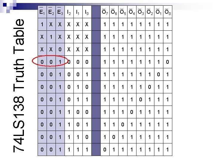
74 LS 138 Truth Table E 1 E 2 E 3 I 2 I 1 I 0 O 7 O 6 O 5 O 4 O 3 O 2 O 1 O 0 1 X X X 1 1 1 1 X 1 X X 1 1 1 1 X X 0 X X X 1 1 1 1 0 0 0 1 1 1 1 0 0 0 1 1 1 1 0 1 0 1 0 1 1 0 0 1 1 1 1 0 0 1 1 1 0 0 1 1 1 0 1 1 1 0 0 1 1 1 1

Conclusion

Conclusion Gates: most basic elements in circuits. n Gates can be extended to perform advanced functions. n Some types are universal (NAND, NOR). n

Conclusion n Flip-flops can store data – feedback: ¨ Can n store previous data. Decoders transform code into original signals. ¨ Used in memory interfacing (Chapter 4).

Tutorial

Tutorial Name three basic gates. n What are extended gates? What’s the difference between extended gates and basic gates? n What is the flip-flop used for? n

Tutorial Describe the RS, JK, D and Asynchronous flip-flops and draw the truth tables for them. n Why are NAND and NOR gates called universal gates? Why are they special? n

Tutorial Give the definition of decoder. n Draw the truth table of the 74 LS 138 and 74 LS 139 decoder. n

The End