The Microprocessor Its Architecture A Course in Microprocessor


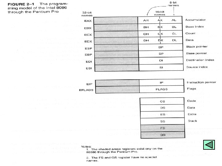
 • Fig. 2. 1 depicts the programming model of the")
 – EBX (base index) registers sometimes hold the offset address")
 – ESI (source index) addresses source string data for the")
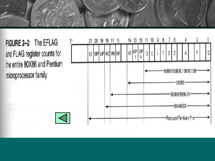
 – EFLAGS indicate the condition of the microprocessor as well")
 • S (sign) flag holds the arithmetic sign of the")
 • NT (nested task) flag indicates that the current task")
 • ID (identification) flag indicates that the Pentium/ Pro µP")
 – DS (data) is a section of memory that contains")

 • The offset address selects any location within the")
 • The µP has a set of rule that")
 – Another of the default combination is the stack")
 • The segment and offset addressing scheme allows both")
- Slides: 23
The Microprocessor & Its Architecture A Course in Microprocessor Electrical Engineering Department Universitas 17 Agustus 1945 Jakarta
Objectives • Describe the function and purpose of each program-visible & program-invisible register • Detail the flag register and the purpose of each flag bit • Describe how memory is accessed using real mode memory-addressing techniques • Describe how memory is accessed using protected mode memory-addressing techniques • Details the operation of the memory paging mechanism
Internal µP Architecture • The programming model of the 8086 through the Pentium Pro is considered program visible because its registers are used during programming and are specified by the instructions • Other registers are considered program invisible because they are not addressable directly during applications programming, but may be used indirectly during system programming
Internal µP Architecture (cont’d) • Fig. 2. 1 depicts the programming model of the 8086 - Pentium Pro microprocessor • The earlier 8086/8/286 contain 16 -bit while 80386/486/Pentium/Pro contain full 32 -bit internal architecture • The multipurpose register include EAX, EBX, ECX, EDX, EBP, EDI, and ESI – EAX (accumulator) is used for instructions (e. g. , multiplication, division, and some of adjustment instructions) and may hold the offset address of a location in the memory
Internal µP Architecture (cont’d) – EBX (base index) registers sometimes hold the offset address of a location in the memory system – ECX (count) holds the account for various instructions – EDX (data) holds a part of the result from a multiplication or a part of the dividend before a division – EBP (base pointer) points to a memory location – EDI (destination index) addresses string destination data for the string instructions
Internal µP Architecture (cont’d) – ESI (source index) addresses source string data for the string instructions • Special Purpose Registers include EIP, ESP, EFLAGS and the segment registers CS, DS, ES, SS, FS, and GS – EIP (instruction pointer) points to the next instruction in a program and is used to find the next sequential instruction in a program located within the code segment – ESP (stack pointer) addresses an area of memory called the stack
Internal µP Architecture (cont’d) – EFLAGS indicate the condition of the microprocessor as well as control its operation (Fig. 2. 2) • C (carry) holds the carry after addition or the borrow after subtraction • P (parity) is a logic 0 for odd parity and a logic 1 for even parity. Parity is a count of ones in a number expressed as even or odd • A (auxiliary carry) holds the carry (half-carry) after addition or the borrow after subtraction between bits position 3 and 4 of the result • Z (zero) flag shows that the result of an arithmetic or logic operation. Z=1, if the result is zero. Z=0, if the result is not zero.
Internal µP Architecture (cont’d) • S (sign) flag holds the arithmetic sign of the result after an arithmetic or logic instruction executes. • T (trap) flag enables trapping through an on-chip debugging feature • I (interrupt) flag controls the operation of the INTR (interrupt request) input pin • D (direction) flag selects either the increment or decrement mode for the DI and/or SI register during string instructions • O (overflow) flag indicates the result of addition or subtraction has exceeded the capacity of the machine • IOPL (I/O privilege level) is used in protected mode operation to select the privilege level for I/O devices
Internal µP Architecture (cont’d) • NT (nested task) flag indicates that the current task is nested within another task in protected mode operation • RF (resume flag) is used with debugging to control the resumption of execution after the next instruction • VM (virtual mode) flag bit selects virtual mode operation in a protected mode system • AC (alignment check) flag bit activates if a word or a doubleword is addressed on a non-word or a nondoubleword boundary • VIF (Virtual Interrupt Flag) is a copy of the interrupt flag bit available to the Pentium/Pro µP • VIP (Virtual Interrupt Pending) provides information about a virtual mode interrupt for the Pentium/Pro µP
Internal µP Architecture (cont’d) • ID (identification) flag indicates that the Pentium/ Pro µP support the CPUID instruction • Segment Registers are additional registers which generate memory addresses when combined with other registers in the µP – CS (code) is a section of memory that holds the code (programs and procedures) used by the µP The code segment register defines the starting address of the section of memory holding code – ES (extra) is an additional data segment used by some of the string instructions to hold destination data
Internal µP Architecture (cont’d) – DS (data) is a section of memory that contains most data used by a program. Data are accessed in the data segment by an offset address or the content of other registers that holds offset address – SS (stack) defines the area of memory used for the stack. The BP register also addresses data within the stack segment
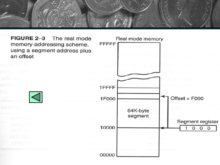
REAL MODE MEMORY ADDRESSING • The 80286 or above operate in either the real or protected mode • Real mode operation allows the µP to address only the first 1 MB of memory space (the real memory or conventional memory) • A combination of a segment address and an offset address access a memory location in the real mode • The segment address defines the beginning address of any 64 K-byte memory segment
REAL MODE MEMORY ADDRESSING (cont’d) • The offset address selects any location within the 64 KB memory segment (Fig. 2. 3) • In the real mode, each segment register is internally appended with a 0 H on its rightmost end. This forms a 20 -bit memory address, allowing it to access the start of a segment at any 16 -byte boundary (a paragraph) within the first 1 MB of memory (i. e. requires 20 -bit memory address)
REAL MODE MEMORY ADDRESSING (cont’d) • The µP has a set of rule that apply to segment whenever memory is addressed – The code segment register is always used with the instruction pointer to address the next instruction in a program (CS: IP or CS: EIP) • The code segment register defines the start of the code segment and the instruction pointer locates the next instruction within the code segment • This combination locates the next instruction executed by the microprocessor
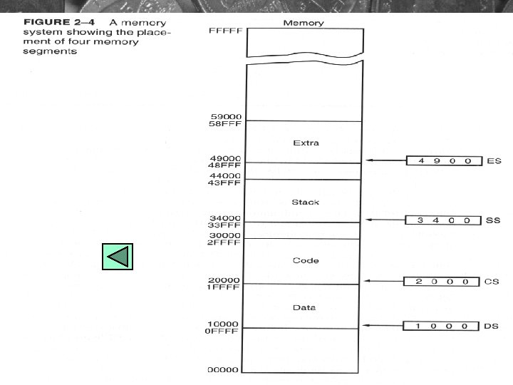
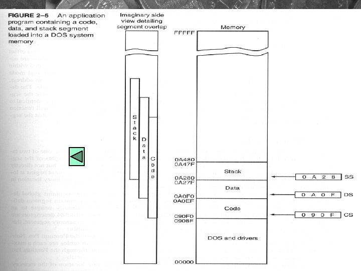
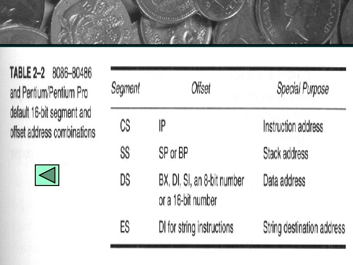
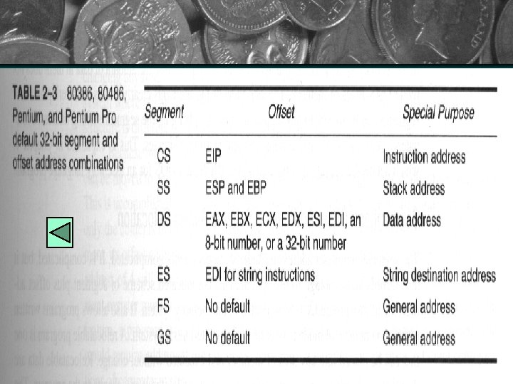
REAL MODE MEMORY ADDRESSING (cont’d) – Another of the default combination is the stack • Stack data are referenced through the stack segment at the memory location addressed by either the stack pointer (SP/ESP) or the base pointer (BP/EBP) • The combinations are referred to as SS: SP or SS: BP – Other default are shown in Table 2 -2 (16 -bit registers) and Table 2 -3 (32 -bit registers) • The 8086 -286 allow four memory segments, and 80386 and above allow six memory segments (fig. 2. 4) • Fig. 2. 5 shows how an application is stored
REAL MODE MEMORY ADDRESSING (cont’d) • The segment and offset addressing scheme allows both program and data to be relocated without changing anything in the programs or data – Because the memory is addressed within a segment by an offset address, the memory segment can be moved to any place in the memory system without changing any of the offset addresses, i. e. , by moving the entire program as a block to a new area and then changing only the contents of the segment registers