History 2 Intel 8086 4004 8008 4004 1


 • Introduced December 2001 •")


 • The")
 • 4004 worked at a clock frequency of")


 registers: 1. Data reg. – to hold data for an")


![CX - Count reg – Loop counter – REP – repeat [in string operations]](https://slidetodoc.com/presentation_image_h/25e2f3a6fdd3f1061f721c28f8c39d87/image-18.jpg "CX - Count reg – Loop counter – REP – repeat [in string operations]")
 registers: 1. Data reg. – to hold data for an")


![CS, DS, SS, ES Machine lang. - instruction [code] - data - stack [data](https://slidetodoc.com/presentation_image_h/25e2f3a6fdd3f1061f721c28f8c39d87/image-28.jpg "CS, DS, SS, ES Machine lang. - instruction [code] - data - stack [data")

 registers: 1. Data reg. – to hold data for an")


![Instruction pointer [IP] reg. Q: Which registers so far are for data access or](https://slidetodoc.com/presentation_image_h/25e2f3a6fdd3f1061f721c28f8c39d87/image-33.jpg "Instruction pointer [IP] reg. Q: Which registers so far are for data access or")

 registers: 1. Data reg. – to hold data for an")


; 1=main registers; 2=segment registers")
- Slides: 39
History – 2 Intel 8086
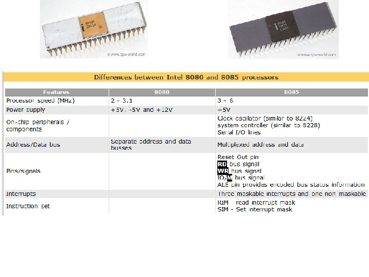
4004 8008 4004 » 1 st 4 -bit microprocessor » 740 KHz » 4 KB program memory » 640 bytes data memory » 3 -level deep stack » No interrupts 16 -pin DIP 8008 » 1 st 8 -bit microprocessor » Up to 800 KHz » 16 KB memory » 7 -level deep stack » 8 In / 24 Out ports 18 -pin DIP
4004 8008 8085 8080 » 8 -bit microprocessor » Up to 3. 1 MHz » 64 KB RAM » Stack in RAM » 256 I/O ports 40 -pin DIP Computers: Altair 8800, IMSAI 8080, Compu. Color II, Byte Computers Byt-8 Related Family: 6800, Z 80 8085 » 8 -bit microprocessor » Up to 8 MHz » 64 KB RAM » Single voltage » On-chip peripherals » 256 I/O ports » 8080 object-code compatib 40 -pin DIP
4004 8008 8085 8086 8085 » 8 -bit microprocessor » Up to 8 MHz » 64 KB RAM » Single voltage » On-chip peripherals » 256 I/O ports » 8080 object-code compatible 40 -pin DIP 8086 » 16 -bit microprocessor » 16 -bit data bus » Up to 10 MHz » 1 MB RAM » 64 K I/O ports 40 -pin DIP
Currently Popular – Intel Pentium 4 (2. 2 GHz) • Introduced December 2001 • 55 million transistors • 32 -bit word size • 2 ALU’s, each working at 4. 4 GHz • 128 -bit FPU • 0. 13 micron process • Targeted use: PC’s and low-end workstations • Cost: around $600
Moore’s Law • In 1965, one of the founders of Intel – Gordon Moore – predicted that the number of transistor on an IC (and therefore the capability of microprocessors) will double every year. Later he modified it to 18 -months • His prediction still holds true in ‘ 02. In fact, the time required for doubling is contracting to the original prediction, and is closer to a year now
Evolution of Intel Microprocessors
4 -, 8 -, 16 -, 32 -, 64 -bit (Word Length) • The 4004 dealt with data in chunks of 4 -bits at a time • Pentium 4 deals with data in chunks (words) of 32 bit length • The new Itanium processor deals with 64 -bit chunks (words) at a time • Why have more bits (longer words)?
k. Hz, MHz, GHz (Clock Frequency) • 4004 worked at a clock frequency of 108 k. Hz • The latest processors have clock freqs. in GHz • Out of 2 u. Ps having similar designs, one with higher clock frequency will be more powerful • Same is not true for 2 u. Ps of dissimilar designs. Example: Out of Power. PC & Pentium 4 u. Ps working at the same freq, the former performs better due to superior design. Same for the Athlon u. P when compared with a Pentium
Enhancing the capability of a u. P? The computing capability of a u. P can be enhanced in many different ways: – By increasing the clock frequency – By increasing the word-width – By having a more effective caching algorithm and the right cache size – By adding more functional units (e. g. ALU’s, FPU’s, Vector/SIMD units, etc. ) – Improving the architecture
Intel 8086: Registers
Registers 14 (16 -bit) registers: 1. Data reg. – to hold data for an op. 2. Address reg – to hold addr of an instruction or data 3. Status reg / FLAGS reg
1. Data reg - 4 • AX • BX • CX • DX High byte – H Low byte – L AX AH + AL
AX – Accumulator reg • Preferred reg to use in arith/logic/data transfer instructions • Multiplication or Division ops. one of the nos. must be in AX or AL • I/O operations also require the use of AX/AL • BX – Base reg: It also serves as an Address reg.
CX - Count reg – Loop counter – REP – repeat [in string operations] – CL as a count in instructions that shift and rotate bits • DX [Data register] – Used in MUX and Division – Used in I/O ops.
Registers 14 (16 -bit) registers: 1. Data reg. – to hold data for an op. 2. Address reg – to hold addr of an instruction or data 3. Status reg / FLAGS reg
2. Address reg. a. Segment reg CS, DS, SS, ES b. Pointer & index reg Si, DI, SP, BP, IP
a. Segment regs. – 4 • Each memory byte has an address • 8086 proc assigns a 20 -bit physical address to its memory locations • It is possible to address 220 = 1, 048, 576 = 1 MB of memory • 1 st byte’s address: 00000000 • 2 nd byte’s address: 000000001 • 3 rd 0000000010 …
In HEX • 00000 • 00001 • 00002. . . • FFFFFh
16 -bit processor! 20 -bit address!! Q. Where lies the problem? ? 20 -bit addresses are bigger to fit in a 16 -bit reg or memory word.
টকর Memory Segment • Partioning memory into segments • A memory segment is a block of 216 or 64 K consecutive memory bytes • Segment number – for each segment • Q: How many bits for a segment number? 16 bits! – as each block has byte of 216
Segment: Offset address • Within a segment, a memory location is specified by giving an offset. Memory location Segment no. + Offset Segment: Offset Logical Address
A 4 FB: 4827 h • offset 4827, within segment A 4 FB Q: How to get 20 -bit physical address? 1. Shift the segment address 4 bits to the left (eqv. to multiplying by 10 h) 2. Add the offset So, the Physical Address for A 4 FB: 4827 h ? ? ?
Logical Address: A 4 FB: 4827 h A 4 F B 0 + 4 8 2 7 A 9 8 2 2 h Physical Address 20 -bit Physical Address 16 -bit Segment [after shifting] + 16 -bit Offset
CS, DS, SS, ES Machine lang. - instruction [code] - data - stack [data structure – used by the proc to implement procedure/function calls] These are loaded into different memory segments, i. Code segment - CS ii. Data segment - DS iii. Stack segment - SS
ES – extra segment reg • If a prog needs to access a second data segment, use the ES register! • At any time – only 4 mem locations addressed by the 4 segment reg [C/D/S/E] are accessible Q: How many memory segments can remain active at a time? only 4 memory segments are active
Registers 14 (16 -bit) registers: 1. Data reg. – to hold data for an op. 2. Address reg – to hold addr of an instruction or data 3. Status reg / FLAGS reg
2. Address reg. a. Segment reg CS, DS, SS, ES b. Pointer & index reg SI, DI, SP, BP, IP
b. Pointer & Index reg. • Stack pointer – SP – with SS [? ? ] to access the stack segment • Base pointer – BP – mainly to access data on the stack. Also to access data in other segments. • Source index – SI – to point to memory locations in the data segment addressed by DS [? ? ] • Destination index – DI same as SI – but for instructions of string operations – to access memory locations – addressed by ES [? ? ]
Instruction pointer [IP] reg. Q: Which registers so far are for data access or to access instructions? All above are for data access! CS [Code segment – under Segment reg. ] contains segment no. of the next instruction. IP contains the offset
• IP is updated each time an instruction is executed – so that it will point to the next instruction. Q: Can IP reg be directly manipulated by an instruction? Unlike other registers - NO!
Registers 14 (16 -bit) registers: 1. Data reg. – to hold data for an op. 2. Address reg – to hold addr of an instruction or data 3. Status reg / FLAGS reg
3. Status Reg. /FLAGS reg. • To indicate the status of the m. P. • 1 flag == 1 bit • Y/N 9 active bits – out of ? ? Bits? Q: Types of flags? Some names? a. Status flags – Zero flag, Carry flag, sign flag, parity, auxiliary flag and overflow flag b. Control flags – interrupt flag, trap flag, direction flag
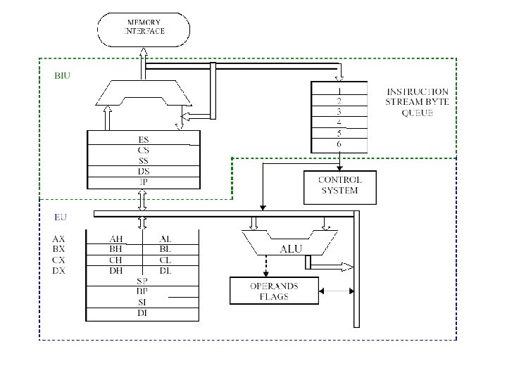
8086 Internal Configuration
Simplified block diagram over Intel 8088 (a variant of 8086); 1=main registers; 2=segment registers and IP; 3=address adder; 4=internal address bus; 5=instruction queue; 6=control unit (very simplified!); 7=bus interface; 8=internal data bus; 9=ALU; 10/11/12=external address/data/control bus