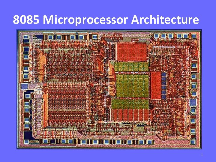
8085 Microprocessor Architecture 1 8085 Microprocessor Architecture v
- Slides: 36

8085 Microprocessor Architecture 1

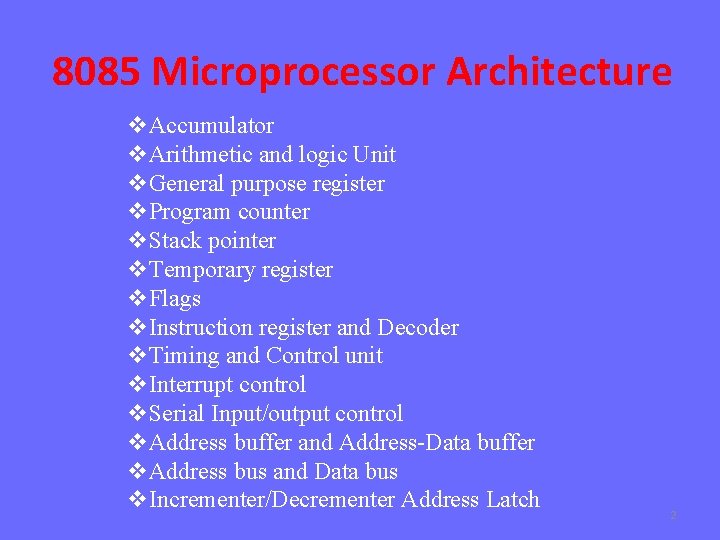
8085 Microprocessor Architecture v. Accumulator v. Arithmetic and logic Unit v. General purpose register v. Program counter v. Stack pointer v. Temporary register v. Flags v. Instruction register and Decoder v. Timing and Control unit v. Interrupt control v. Serial Input/output control v. Address buffer and Address-Data buffer v. Address bus and Data bus v. Incrementer/Decrementer Address Latch 2

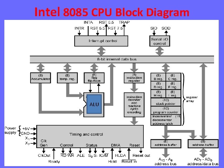
Intel 8085 CPU Block Diagram ALU 3

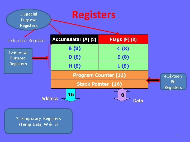
Registers 3. Special Purpose Registers Instruction Registers Accumulator (A) (8) Flags (F) (8) B (8) C (8) D (8) E (8) H (8) L (8) 1. General Purpose Registers Program Counter (16) 4. Sixteen Bit Registers Stack Pointer (16) Address 16 8 Data 2. Temporary Registers (Temp Data, W & Z) 4

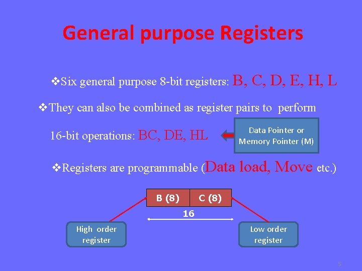
General purpose Registers v. Six general purpose 8 -bit registers: B, C, D, E, H, L v. They can also be combined as register pairs to perform 16 -bit operations: BC, DE, HL Data Pointer or Memory Pointer (M) v. Registers are programmable (Data load, Move etc. ) C (8) B (8) 16 High order register Low order register 5

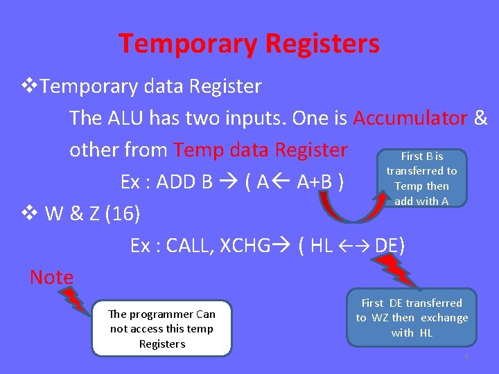
Temporary Registers v. Temporary data Register The ALU has two inputs. One is Accumulator & other from Temp data Register First B is transferred to Ex : ADD B ( A A+B ) Temp then add with A v W & Z (16) Ex : CALL, XCHG ( HL DE) Note The programmer Can not access this temp Registers First DE transferred to WZ then exchange with HL 6

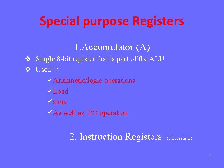
Special purpose Registers 1. Accumulator (A) v Single 8 -bit register that is part of the ALU v Used in üArithmetic/logic operations üLoad üstore üAs well as I/O operation 2. Instruction Registers (Discuss later) 7

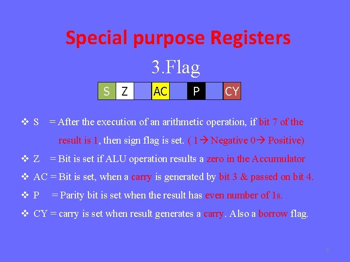
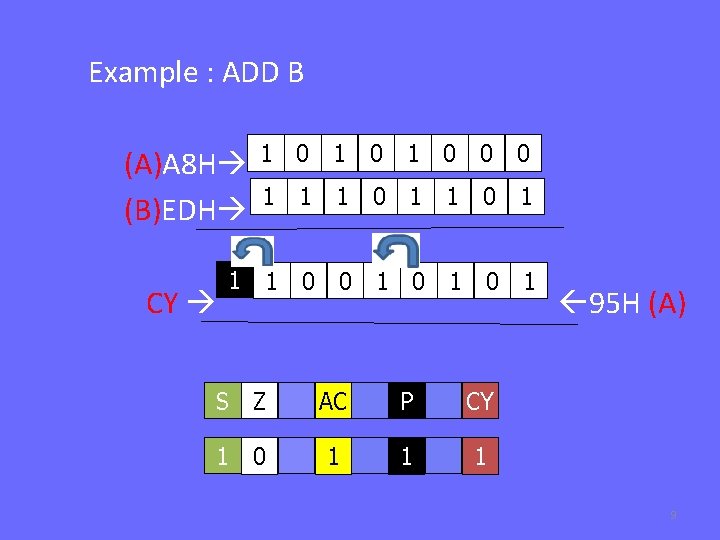
Special purpose Registers 3. Flag S Z AC P CY v S = After the execution of an arithmetic operation, if bit 7 of the result is 1, then sign flag is set. ( 1 Negative 0 Positive) v Z = Bit is set if ALU operation results a zero in the Accumulator v AC = Bit is set, when a carry is generated by bit 3 & passed on bit 4. v. P = Parity bit is set when the result has even number of 1 s. v CY = carry is set when result generates a carry. Also a borrow flag. 8

Example : ADD B (A)A 8 H (B)EDH CY 1 1 0 1 0 0 0 1 1 1 0 0 1 0 1 S Z AC P CY 1 0 1 1 1 95 H (A) 9

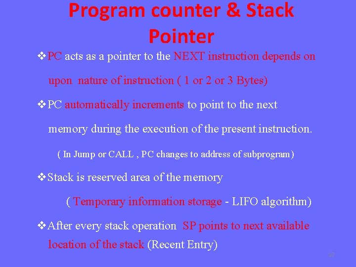
Program counter & Stack Pointer v. PC acts as a pointer to the NEXT instruction depends on upon nature of instruction ( 1 or 2 or 3 Bytes) v. PC automatically increments to point to the next memory during the execution of the present instruction. ( In Jump or CALL , PC changes to address of subprogram) v. Stack is reserved area of the memory ( Temporary information storage - LIFO algorithm) v. After every stack operation SP points to next available location of the stack (Recent Entry) 10

ALU (Arithmetic & Logic Unit) v To perform arithmetic operations like Addition & Subtraction v To perform logical operations like üAND üOR üNOT (Complement) 11

Instruction Register & Decoder v. The processor first fetches the opcode of instruction from memory & stores opcode in the instructions registers , it is then sent to instruction decoder v. The Instruction decoder decodes the it & accordingly gives for further processing depending on nature of instructions 12

Address buffer & Address/Data buffer Address Buffer v 8 bit unidirectional buffer v. The address bits are always sent from the MPU to peripheral devices, not reverse v. Used to drive external High order address bus (A 8 -A 15) Address Buffer & Address/Data Buffer v 8 bit Bidirectional buffer v. The data bits are sent from the MPU to peripheral devices, as well as from the peripheral devices to the MPU v. Used to drive multiplexed address/data bus i. e Low order address bus (A 0 -A 7) & data bus (D 0 -D 7) 13

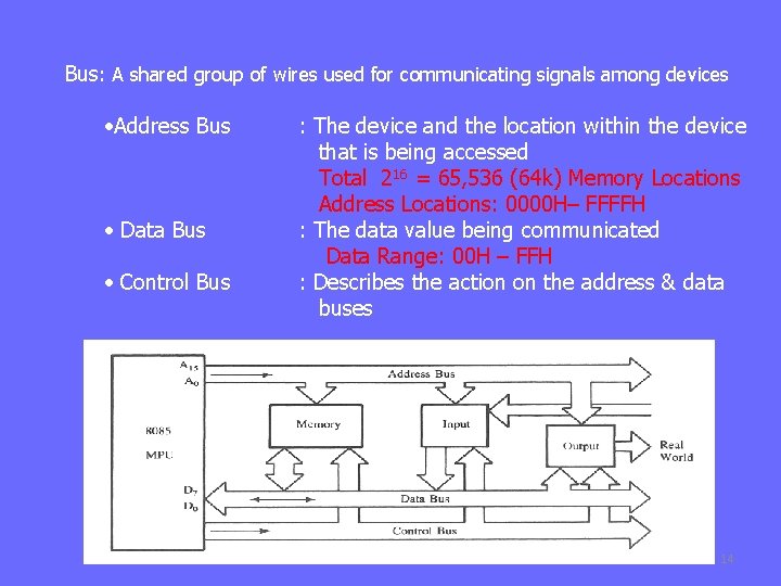
Bus: A shared group of wires used for communicating signals among devices • Address Bus • Data Bus • Control Bus : The device and the location within the device that is being accessed Total 216 = 65, 536 (64 k) Memory Locations Address Locations: 0000 H– FFFFH : The data value being communicated Data Range: 00 H – FFH : Describes the action on the address & data buses 14

Incrementer/ Decrementer Address Latch v. This 16 bit Register is used to increment or decrement the contents of the PC or SP as a part of execution instructions related to them 15

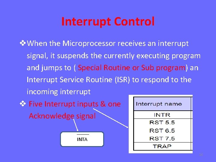
Interrupt Control v. When the Microprocessor receives an interrupt signal, it suspends the currently executing program and jumps to ( Special Routine or Sub program) an Interrupt Service Routine (ISR) to respond to the incoming interrupt v Five Interrupt inputs & one Acknowledge signal INTA 16

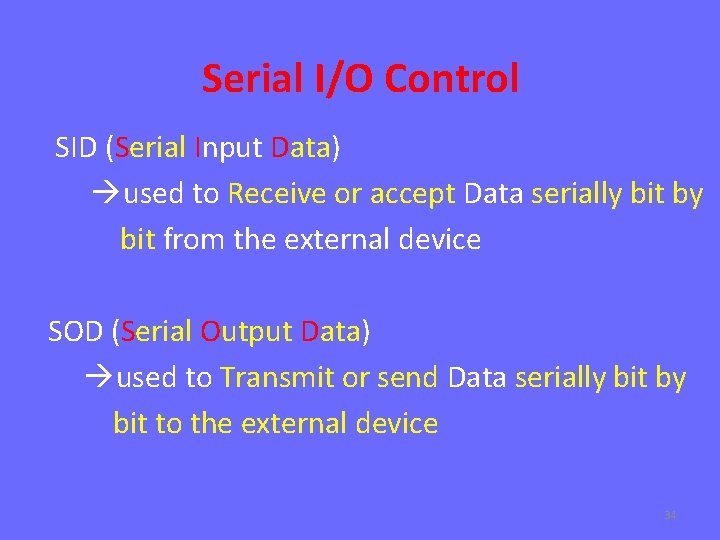
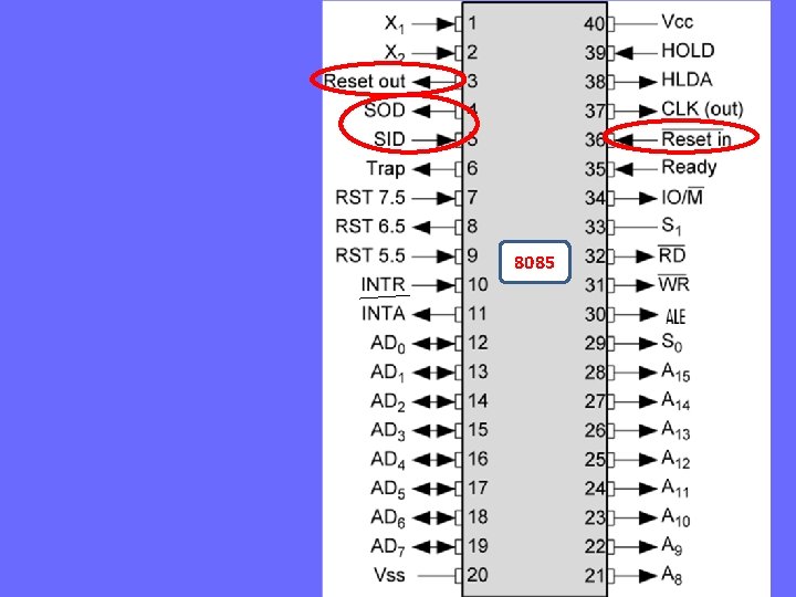
Serial I/O Control v. It provides two lines SOD & SID for Serial Communication 1. SOD (Serial Output Data) used to send Data serially 2. SID (Serial Input Data) used to Receive Data serially 17

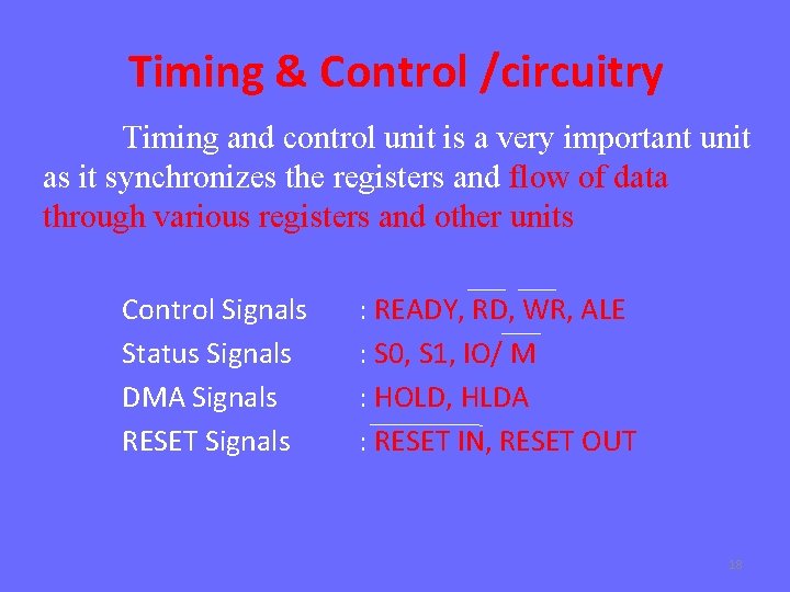
Timing & Control /circuitry Timing and control unit is a very important unit as it synchronizes the registers and flow of data through various registers and other units Control Signals Status Signals DMA Signals RESET Signals : READY, RD, WR, ALE : S 0, S 1, IO/ M : HOLD, HLDA : RESET IN, RESET OUT 18

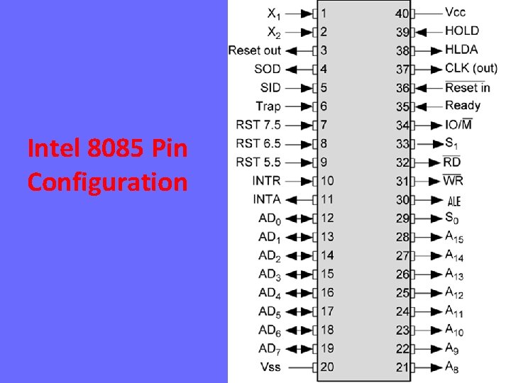
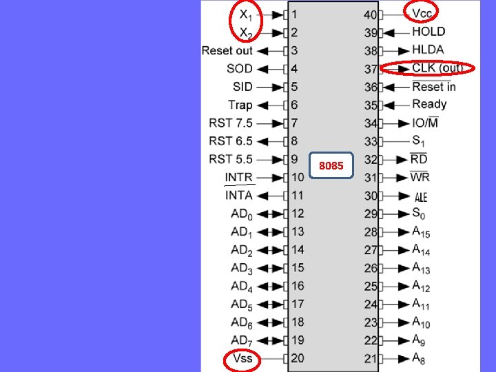
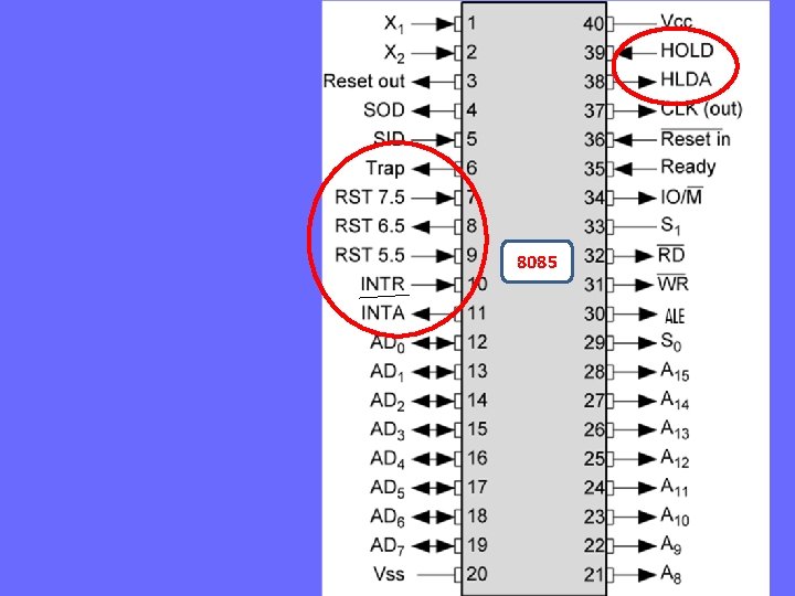
Intel 8085 Pin Configuration 8085 19

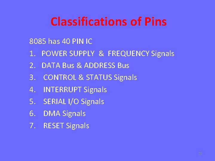
Classifications of Pins 8085 has 40 PIN IC 1. POWER SUPPLY & FREQUENCY Signals 2. DATA Bus & ADDRESS Bus 3. CONTROL & STATUS Signals 4. INTERRUPT Signals 5. SERIAL I/O Signals 6. DMA Signals 7. RESET Signals 20

8085 21

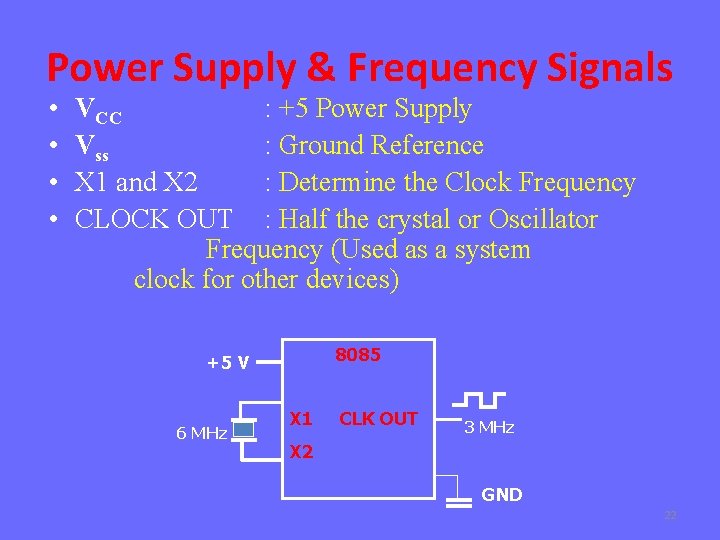
Power Supply & Frequency Signals • • VCC : +5 Power Supply Vss : Ground Reference X 1 and X 2 : Determine the Clock Frequency CLOCK OUT : Half the crystal or Oscillator Frequency (Used as a system clock for other devices) 8085 +5 V 6 MHz X 1 CLK OUT 3 MHz X 2 GND 22

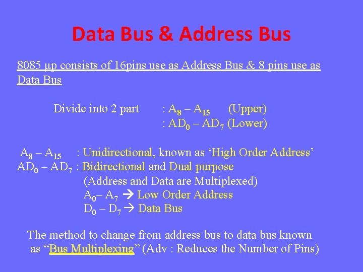
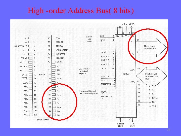
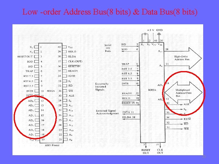
Data Bus & Address Bus 8085 μp consists of 16 pins use as Address Bus & 8 pins use as Data Bus Divide into 2 part : A 8 – A 15 (Upper) : AD 0 – AD 7 (Lower) A 8 – A 15 : Unidirectional, known as ‘High Order Address’ AD 0 – AD 7 : Bidirectional and Dual purpose (Address and Data are Multiplexed) A 0– A 7 Low Order Address D 0 – D 7 Data Bus The method to change from address bus to data bus known as “Bus Multiplexing” Multiplexing (Adv : Reduces the Number of Pins)

High -order Address Bus( 8 bits) 24

Low -order Address Bus(8 bits) & Data Bus(8 bits) 25

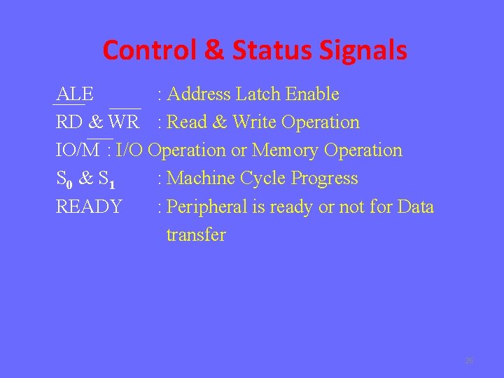
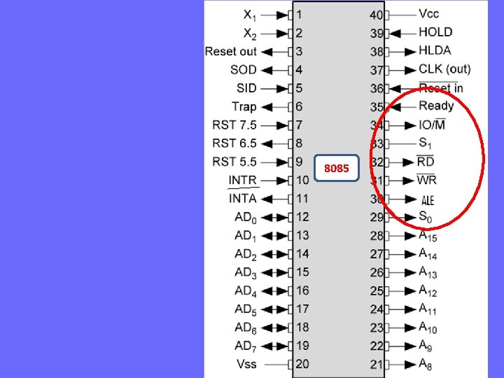
Control & Status Signals ALE : Address Latch Enable RD & WR : Read & Write Operation IO/M : I/O Operation or Memory Operation S 0 & S 1 : Machine Cycle Progress READY : Peripheral is ready or not for Data transfer 26

8085 27

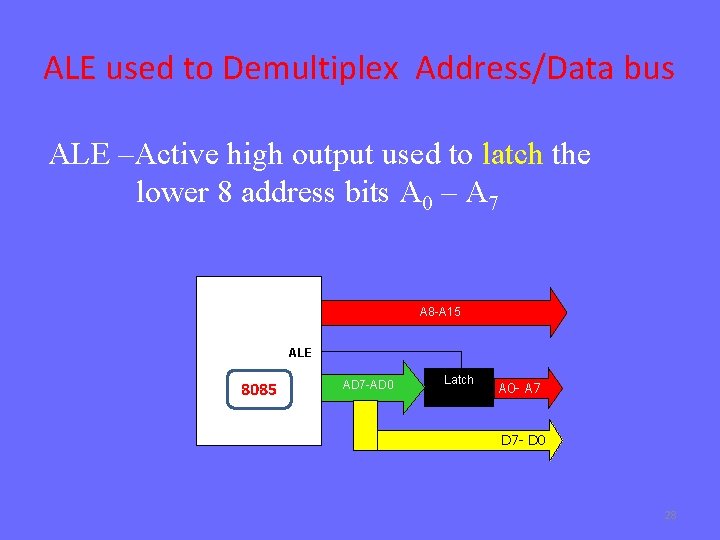
ALE used to Demultiplex Address/Data bus ALE –Active high output used to latch the lower 8 address bits A 0 – A 7 A 8 -A 15 ALE 8085 AD 7 -AD 0 Latch A 0 - A 7 D 7 - D 0 28

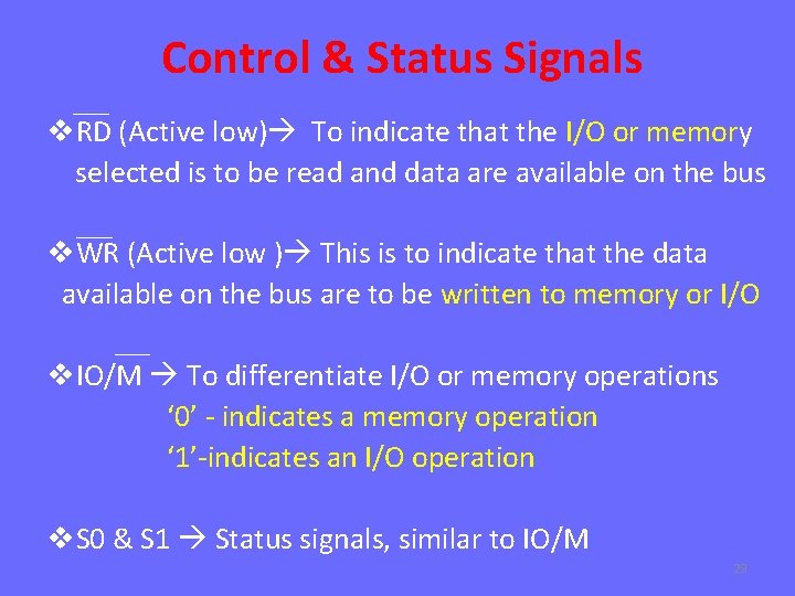
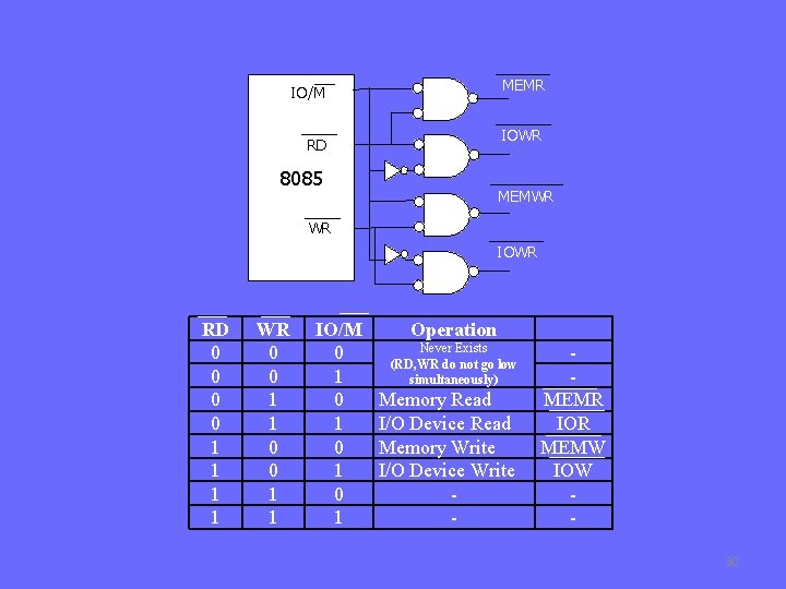
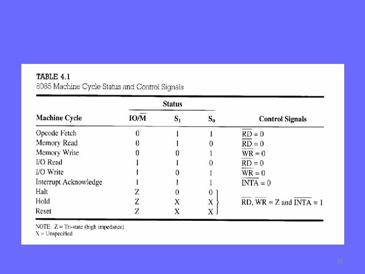
Control & Status Signals v. RD (Active low) To indicate that the I/O or memory selected is to be read and data are available on the bus v. WR (Active low ) This is to indicate that the data available on the bus are to be written to memory or I/O v. IO/M To differentiate I/O or memory operations ‘ 0’ - indicates a memory operation ‘ 1’-indicates an I/O operation v. S 0 & S 1 Status signals, similar to IO/M 29

MEMR IO/M IOWR RD 8085 MEMWR WR IOWR RD 0 0 1 1 WR 0 0 1 1 IO/M 0 1 0 1 Operation Never Exists (RD, WR do not go low simultaneously) Memory Read I/O Device Read Memory Write I/O Device Write - MEMR IOR MEMW IOW 30

31

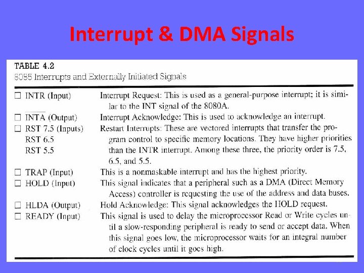
Interrupt & DMA Signals 32

8085 33

Serial I/O Control SID (Serial Input Data) used to Receive or accept Data serially bit by bit from the external device SOD (Serial Output Data) used to Transmit or send Data serially bit by bit to the external device 34

8085 35

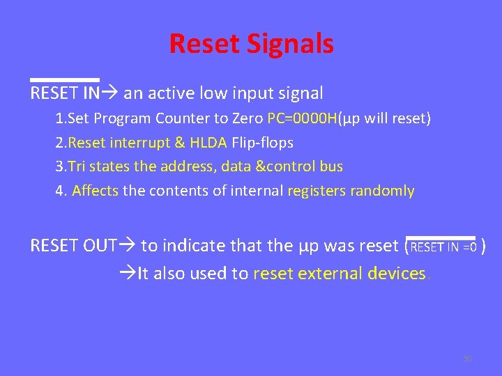
Reset Signals RESET IN an active low input signal 1. Set Program Counter to Zero PC=0000 H(μp will reset) 2. Reset interrupt & HLDA Flip-flops 3. Tri states the address, data &control bus 4. Affects the contents of internal registers randomly RESET OUT to indicate that the μp was reset (RESET IN =0 ) It also used to reset external devices. 36