MICROPROCESSOR SYSTEMS Week4 8085 Working Animation 8086 ARCHITECTURE


- Slides: 37

MICROPROCESSOR SYSTEMS Week-4

8085 Working Animation

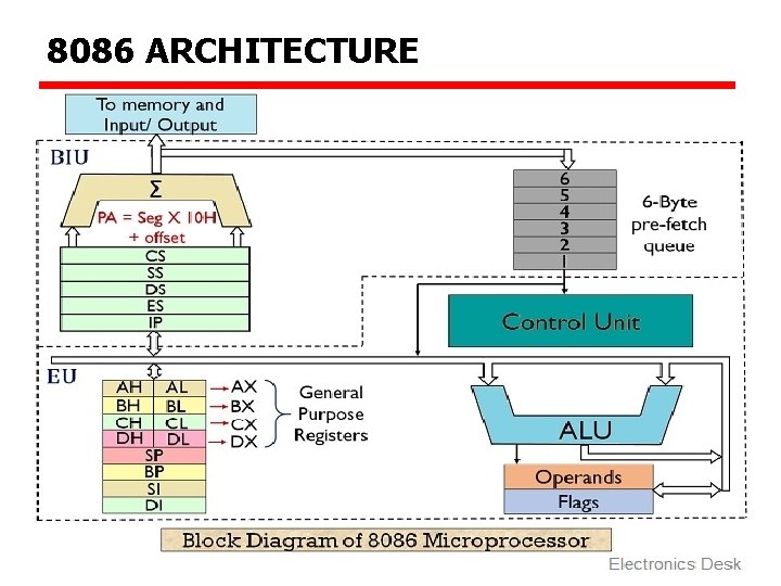
8086 ARCHITECTURE

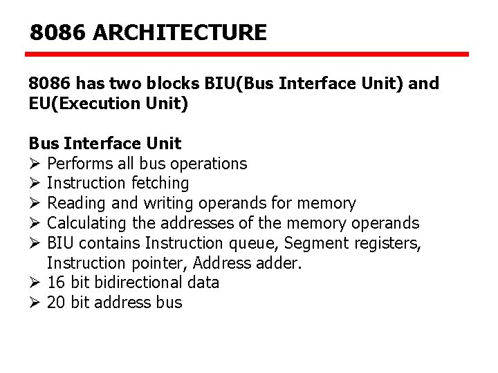
8086 ARCHITECTURE 8086 has two blocks BIU(Bus Interface Unit) and EU(Execution Unit) Bus Interface Unit Ø Performs all bus operations Ø Instruction fetching Ø Reading and writing operands for memory Ø Calculating the addresses of the memory operands Ø BIU contains Instruction queue, Segment registers, Instruction pointer, Address adder. Ø 16 bit bidirectional data Ø 20 bit address bus

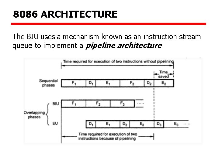
8086 ARCHITECTURE The BIU uses a mechanism known as an instruction stream queue to implement a pipeline architecture

8086 ARCHITECTURE Execution Unit Ø Instruction bytes are transferred to the instruction queue Ø EU executes instructions from the instruction system byte queue Ø Both units operate asynchronously to give the 8086 an overlapping instruction fetch and execution mechanism which is called as Pipelining Ø Results in efficient use of the system bus and system performance Ø EU contains Control circuitry, Instruction decoder, ALU, Pointer and Index register, Flag register

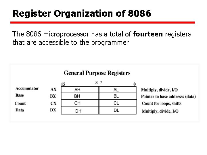
Register Organization of 8086 The 8086 microprocessor has a total of fourteen registers that are accessible to the programmer

Register Organization of 8086 Accumulator Register Ø Consists of two 8 -bit registers AL and AH Ø Can be combined together and used as a 16 -bit register AX Ø AL in this case contains the low-order byte of the word Ø AH contains the high-order byte Ø Accumulator can be used for I/O operations and string manipulation.

Register Organization of 8086 Base Register Ø Base register consists of two 8 -bit registers BL and BH Ø Can be combined together and used as a 16 -bit register BX Ø BL in this case contains the low-order byte of the word Ø BH contains the high-order byte Ø BX register usually contains a data pointer used for based, based indexed or register indirect addressing

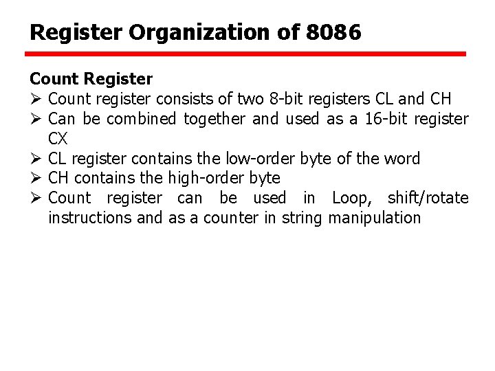
Register Organization of 8086 Count Register Ø Count register consists of two 8 -bit registers CL and CH Ø Can be combined together and used as a 16 -bit register CX Ø CL register contains the low-order byte of the word Ø CH contains the high-order byte Ø Count register can be used in Loop, shift/rotate instructions and as a counter in string manipulation

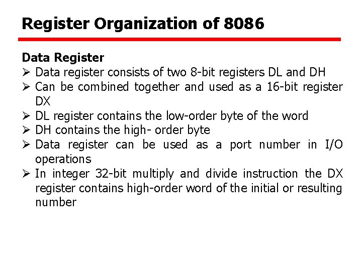
Register Organization of 8086 Data Register Ø Data register consists of two 8 -bit registers DL and DH Ø Can be combined together and used as a 16 -bit register DX Ø DL register contains the low-order byte of the word Ø DH contains the high- order byte Ø Data register can be used as a port number in I/O operations Ø In integer 32 -bit multiply and divide instruction the DX register contains high-order word of the initial or resulting number

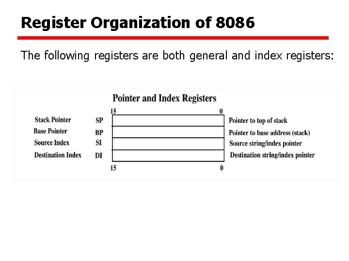
Register Organization of 8086 The following registers are both general and index registers:

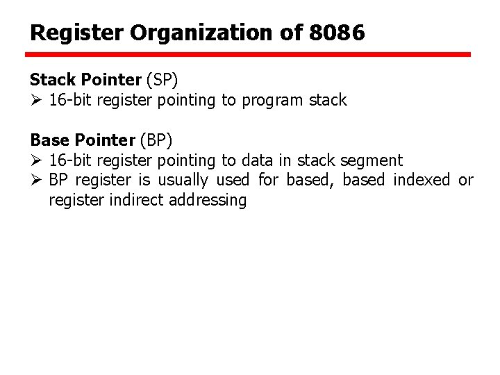
Register Organization of 8086 Stack Pointer (SP) Ø 16 -bit register pointing to program stack Base Pointer (BP) Ø 16 -bit register pointing to data in stack segment Ø BP register is usually used for based, based indexed or register indirect addressing

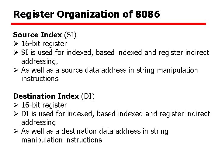
Register Organization of 8086 Source Index (SI) Ø 16 -bit register Ø SI is used for indexed, based indexed and register indirect addressing, Ø As well as a source data address in string manipulation instructions Destination Index (DI) Ø 16 -bit register Ø DI is used for indexed, based indexed and register indirect addressing Ø As well as a destination data address in string manipulation instructions

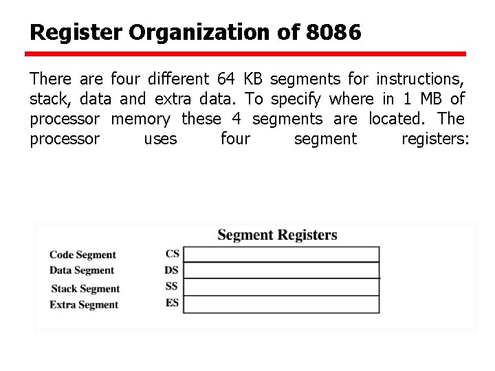
Register Organization of 8086 There are four different 64 KB segments for instructions, stack, data and extra data. To specify where in 1 MB of processor memory these 4 segments are located. The processor uses four segment registers:

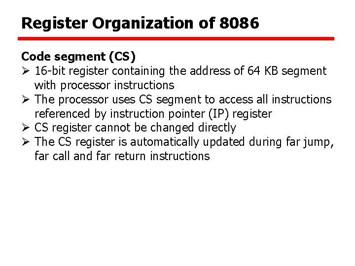
Register Organization of 8086 Code segment (CS) Ø 16 -bit register containing the address of 64 KB segment with processor instructions Ø The processor uses CS segment to access all instructions referenced by instruction pointer (IP) register Ø CS register cannot be changed directly Ø The CS register is automatically updated during far jump, far call and far return instructions

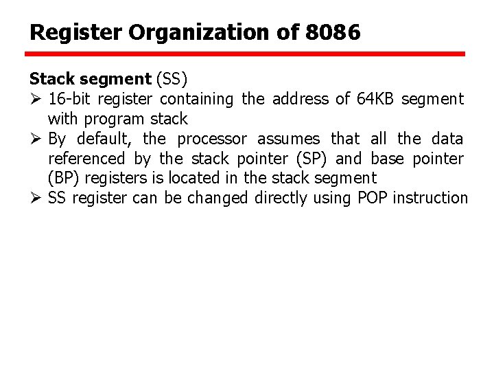
Register Organization of 8086 Stack segment (SS) Ø 16 -bit register containing the address of 64 KB segment with program stack Ø By default, the processor assumes that all the data referenced by the stack pointer (SP) and base pointer (BP) registers is located in the stack segment Ø SS register can be changed directly using POP instruction

Register Organization of 8086 Data segment (DS) Ø 16 -bit register containing address of 64 KB segment with program data Ø By default, the processor assumes that all data referenced by general registers (AX, BX, CX, DX) and index register (SI, DI) is located in the data segment Ø DS register can be changed directly using POP and LDS instructions

Register Organization of 8086 Extra segment (ES) Ø 16 -bit register containing address of 64 KB segment, usually with program data Ø By default, the processor assumes that the DI register references the ES segment in string manipulation instructions Ø ES register can be changed directly using POP and LES instructions Ø It is possible to change default segments used by general and index registers by prefixing instructions with a CS, SS, DS or ES prefix

Other Registers The two remaining registers are the instruction pointer (IP) and the status word, or flags register. Neither of these is referenced directly by your program Instruction Pointer (IP) Ø 16 -bit register Ø Used to control instruction the CPU executes Ø IP or program counter, is used to store the memory location of the next instruction to be executed

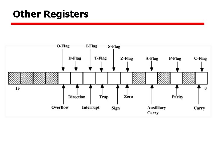
Other Registers Flag Register Ø 16 -bit register containing 9 one bit flags Ø The status flags are used to record specific characteristics of arithmetic and of logical instructions Overflow Flag (OF) - set if the result is too large positive number, or is too small negative number to fit into destination operand. Direction Flag (DF) - if set then string manipulation instructions will auto-decrement index registers. If cleared then the index registers will be auto-incremented. Interrupt-enable Flag (IF) - setting this bit enables mask able interrupts. Trap Flag (TF) - if set then Trap interrupt will occur after the next instruction.

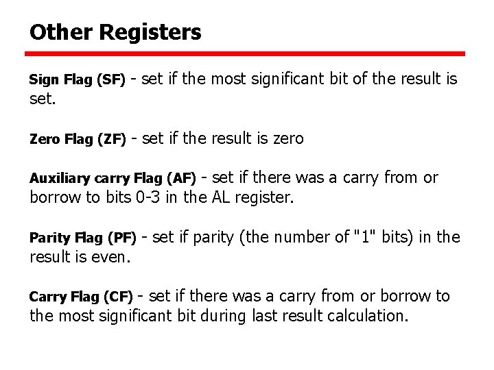
Other Registers Sign Flag (SF) - set if the most significant bit of the result is Zero Flag (ZF) - set if the result is zero set. - set if there was a carry from or borrow to bits 0 -3 in the AL register. Auxiliary carry Flag (AF) Parity Flag (PF) result is even. - set if parity (the number of "1" bits) in the - set if there was a carry from or borrow to the most significant bit during last result calculation. Carry Flag (CF)

Other Registers

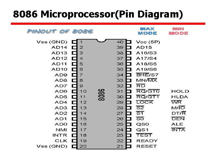
8086 Microprocessor(Pin Diagram)

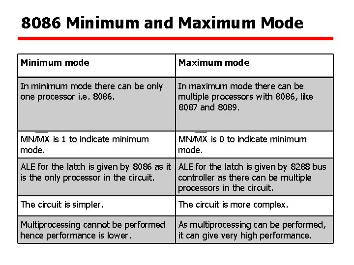
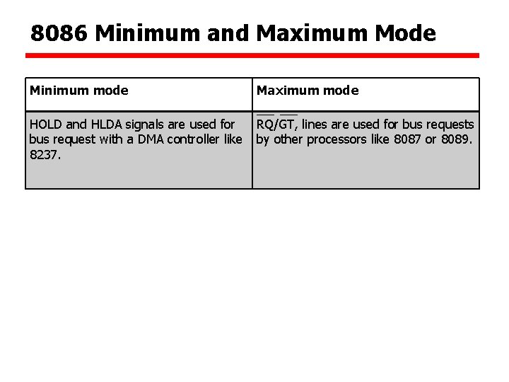
8086 Minimum and Maximum Mode Minimum mode Maximum mode In minimum mode there can be only one processor i. e. 8086. In maximum mode there can be multiple processors with 8086, like 8087 and 8089. MN/MX is 1 to indicate minimum mode. MN/MX is 0 to indicate minimum mode. ALE for the latch is given by 8086 as it ALE for the latch is given by 8288 bus is the only processor in the circuit. controller as there can be multiple processors in the circuit. The circuit is simpler. The circuit is more complex. Multiprocessing cannot be performed hence performance is lower. As multiprocessing can be performed, it can give very high performance.

8086 Minimum and Maximum Mode Minimum mode Maximum mode HOLD and HLDA signals are used for bus request with a DMA controller like 8237. RQ/GT, lines are used for bus requests by other processors like 8087 or 8089.

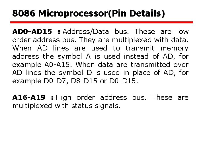
8086 Microprocessor(Pin Details) AD 0 -AD 15 : Address/Data bus. These are low order address bus. They are multiplexed with data. When AD lines are used to transmit memory address the symbol A is used instead of AD, for example A 0 -A 15. When data are transmitted over AD lines the symbol D is used in place of AD, for example D 0 -D 7, D 8 -D 15 or D 0 -D 15. A 16 -A 19 : High order address bus. These are multiplexed with status signals.

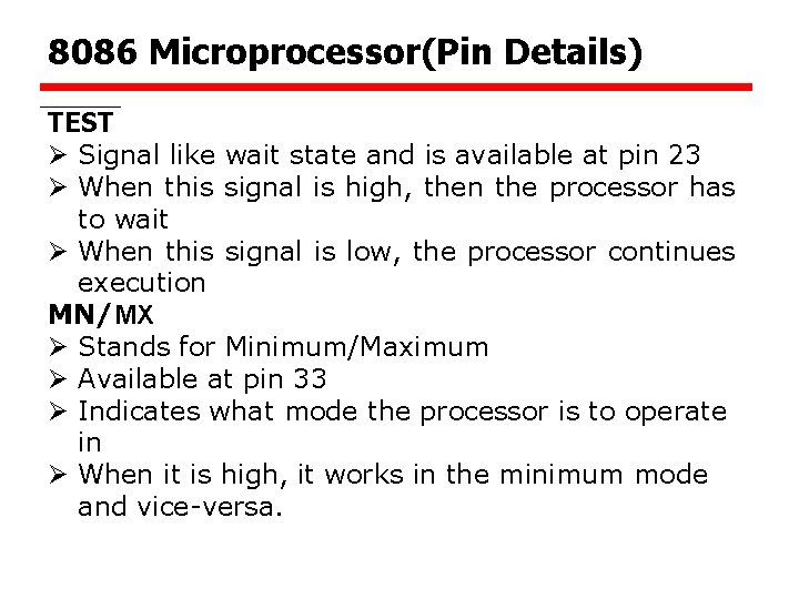
8086 Microprocessor(Pin Details) TEST Ø Signal like wait state and is available at pin 23 Ø When this signal is high, then the processor has to wait Ø When this signal is low, the processor continues execution MN/MX Ø Stands for Minimum/Maximum Ø Available at pin 33 Ø Indicates what mode the processor is to operate in Ø When it is high, it works in the minimum mode and vice-versa.

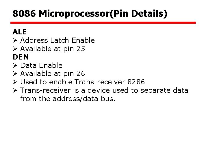
8086 Microprocessor(Pin Details) ALE Ø Address Latch Enable Ø Available at pin 25 DEN Ø Data Enable Ø Available at pin 26 Ø Used to enable Trans-receiver 8286 Ø Trans-receiver is a device used to separate data from the address/data bus.

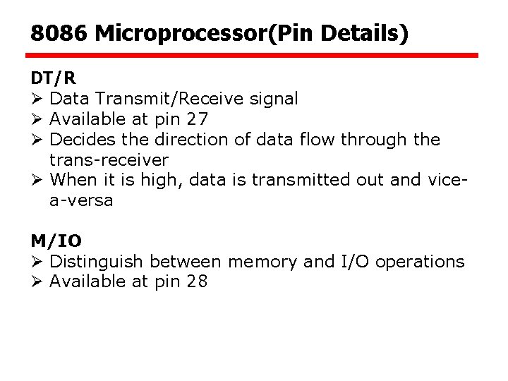
8086 Microprocessor(Pin Details) DT/R Ø Data Transmit/Receive signal Ø Available at pin 27 Ø Decides the direction of data flow through the trans-receiver Ø When it is high, data is transmitted out and vicea-versa M/IO Ø Distinguish between memory and I/O operations Ø Available at pin 28

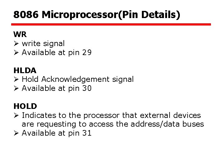
8086 Microprocessor(Pin Details) WR Ø write signal Ø Available at pin 29 HLDA Ø Hold Acknowledgement signal Ø Available at pin 30 HOLD Ø Indicates to the processor that external devices are requesting to access the address/data buses Ø Available at pin 31

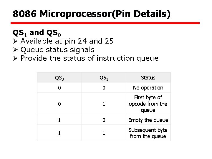
8086 Microprocessor(Pin Details) QS 1 and QS 0 Ø Available at pin 24 and 25 Ø Queue status signals Ø Provide the status of instruction queue QS 0 QS 1 Status 0 0 No operation 0 1 First byte of opcode from the queue 1 0 Empty the queue 1 1 Subsequent byte from the queue

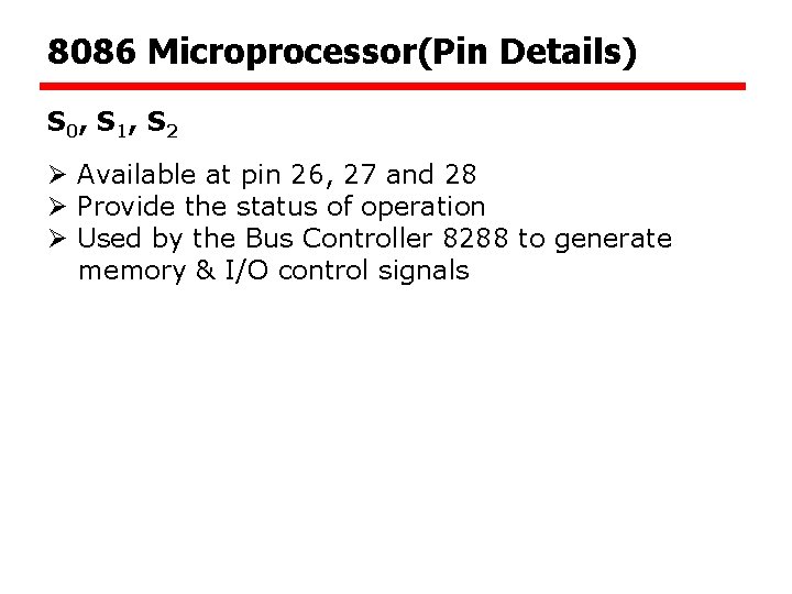
8086 Microprocessor(Pin Details) S 0 , S 1 , S 2 Ø Available at pin 26, 27 and 28 Ø Provide the status of operation Ø Used by the Bus Controller 8288 to generate memory & I/O control signals

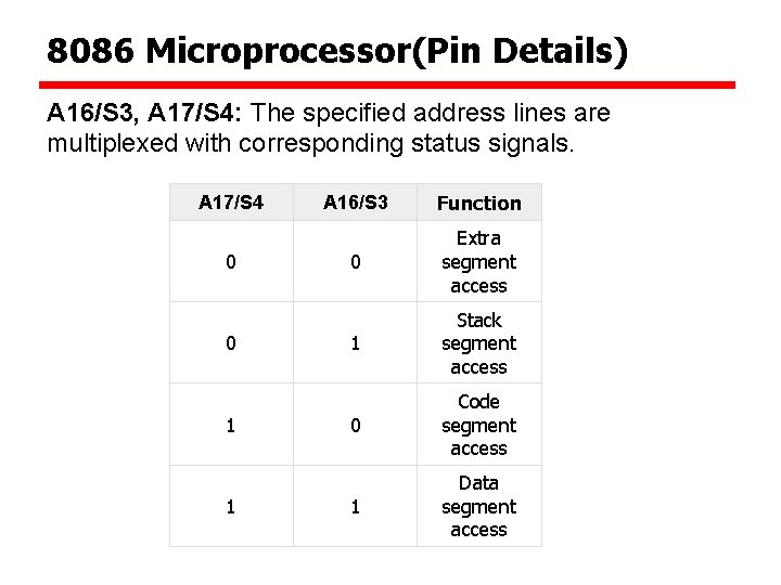
8086 Microprocessor(Pin Details) A 16/S 3, A 17/S 4: The specified address lines are multiplexed with corresponding status signals. A 17/S 4 0 0 1 1 A 16/S 3 Function 0 Extra segment access 1 Stack segment access 0 Code segment access 1 Data segment access

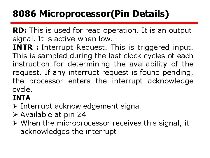
8086 Microprocessor(Pin Details) RD: This is used for read operation. It is an output signal. It is active when low. INTR : Interrupt Request. This is triggered input. This is sampled during the last clock cycles of each instruction for determining the availability of the request. If any interrupt request is found pending, the processor enters the interrupt acknowledge cycle. INTA Ø Interrupt acknowledgement signal Ø Available at pin 24 Ø When the microprocessor receives this signal, it acknowledges the interrupt

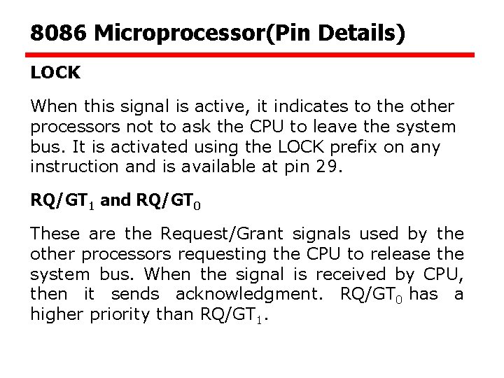
8086 Microprocessor(Pin Details) LOCK When this signal is active, it indicates to the other processors not to ask the CPU to leave the system bus. It is activated using the LOCK prefix on any instruction and is available at pin 29. RQ/GT 1 and RQ/GT 0 These are the Request/Grant signals used by the other processors requesting the CPU to release the system bus. When the signal is received by CPU, then it sends acknowledgment. RQ/GT 0 has a higher priority than RQ/GT 1.

REVIEW