TK 2633 8085 IO Peripherals Interface DR MASRI

- Slides: 17

TK 2633 8085 I/O Peripherals Interface DR MASRI AYOB

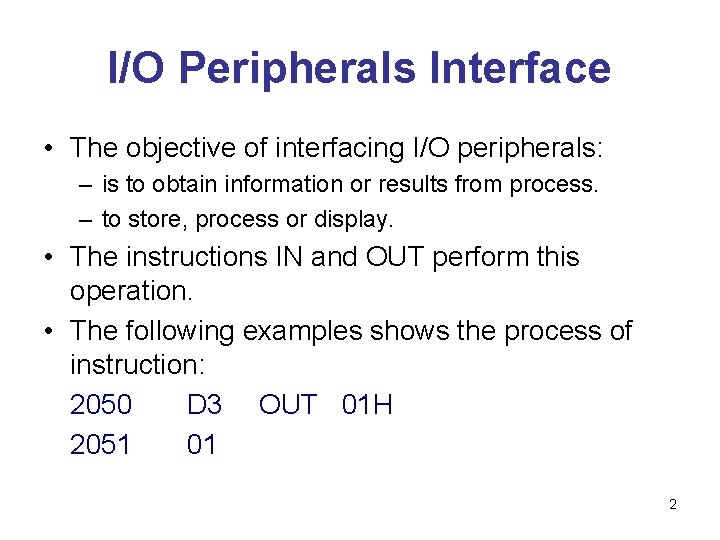
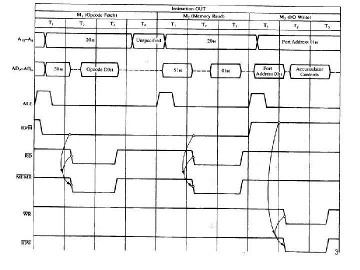
I/O Peripherals Interface • The objective of interfacing I/O peripherals: – is to obtain information or results from process. – to store, process or display. • The instructions IN and OUT perform this operation. • The following examples shows the process of instruction: 2050 D 3 OUT 01 H 2051 01 2

3

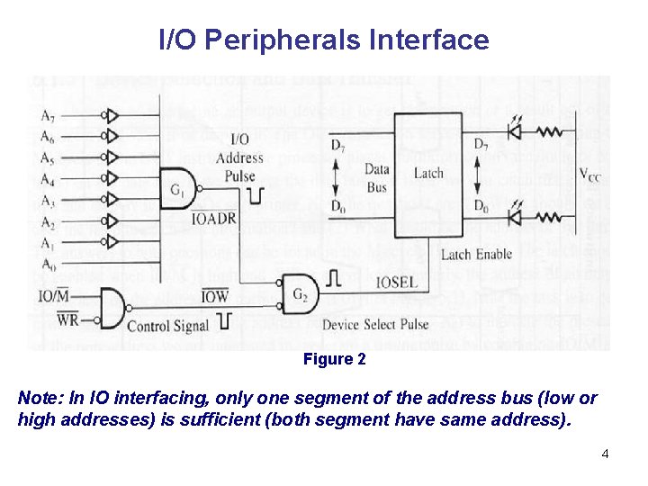
I/O Peripherals Interface Figure 2 Note: In IO interfacing, only one segment of the address bus (low or high addresses) is sufficient (both segment have same address). 4

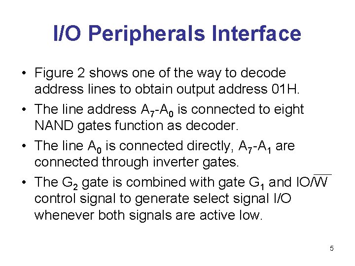
I/O Peripherals Interface • Figure 2 shows one of the way to decode address lines to obtain output address 01 H. • The line address A 7 -A 0 is connected to eight NAND gates function as decoder. • The line A 0 is connected directly, A 7 -A 1 are connected through inverter gates. • The G 2 gate is combined with gate G 1 and IO/W control signal to generate select signal I/O whenever both signals are active low. 5

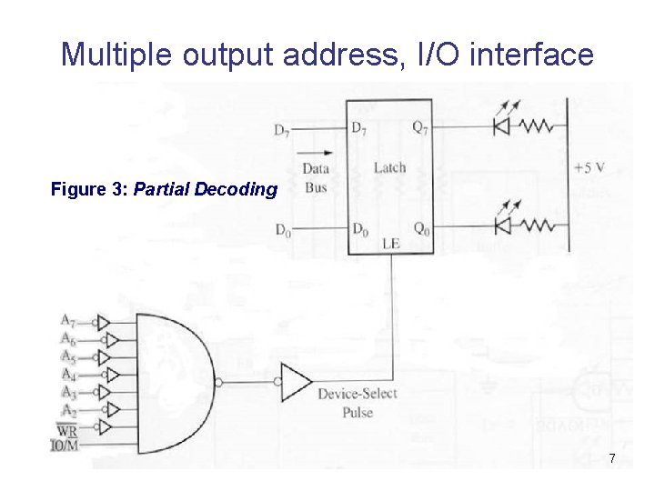
Multiple output address, I/O interface • Figure 2 have shown the technique to decode I/O output address in absolute decoding technique. • There is another technique which is cost saving - partial decoding. • This technique gives the flexibility to user as to use more than one addresses to one output or input device. 6

Multiple output address, I/O interface Figure 3: Partial Decoding 7

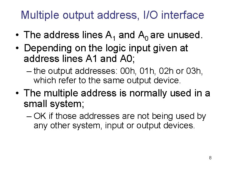
Multiple output address, I/O interface • The address lines A 1 and A 0 are unused. • Depending on the logic input given at address lines A 1 and A 0; – the output addresses: 00 h, 01 h, 02 h or 03 h, which refer to the same output device. • The multiple address is normally used in a small system; – OK if those addresses are not being used by any other system, input or output devices. 8

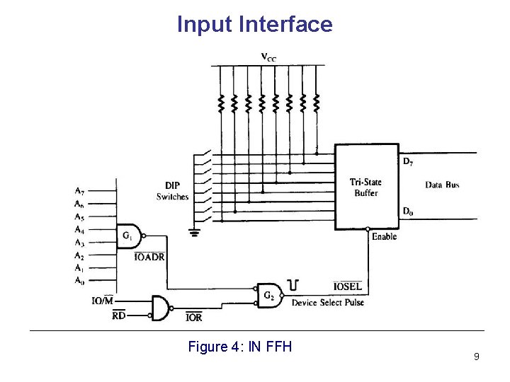
Input Interface Figure 4: IN FFH 9

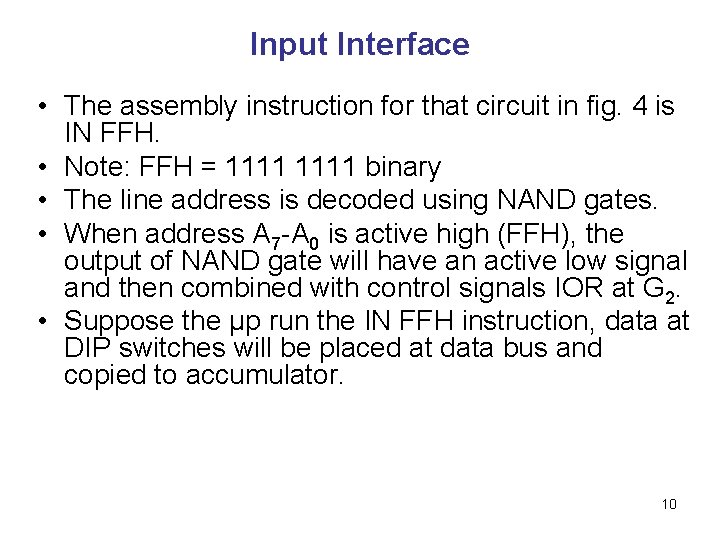
Input Interface • The assembly instruction for that circuit in fig. 4 is IN FFH. • Note: FFH = 1111 binary • The line address is decoded using NAND gates. • When address A 7 -A 0 is active high (FFH), the output of NAND gate will have an active low signal and then combined with control signals IOR at G 2. • Suppose the μp run the IN FFH instruction, data at DIP switches will be placed at data bus and copied to accumulator. 10

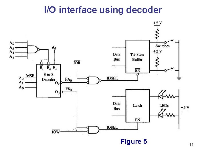
I/O interface using decoder Figure 5 11

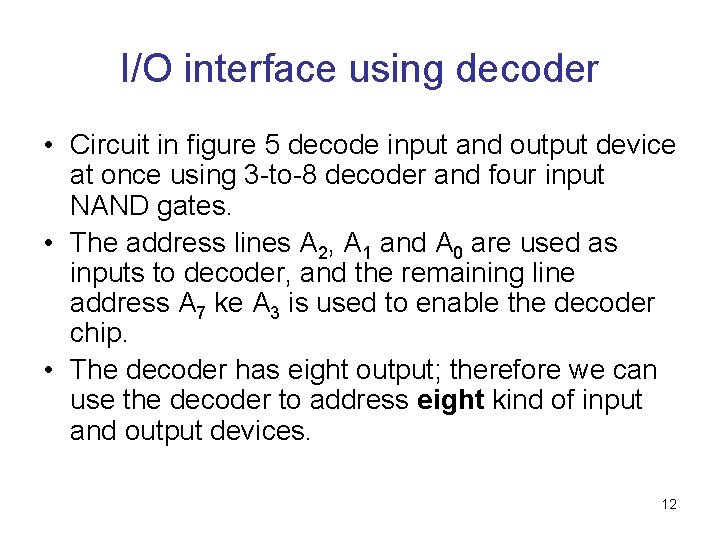
I/O interface using decoder • Circuit in figure 5 decode input and output device at once using 3 -to-8 decoder and four input NAND gates. • The address lines A 2, A 1 and A 0 are used as inputs to decoder, and the remaining line address A 7 ke A 3 is used to enable the decoder chip. • The decoder has eight output; therefore we can use the decoder to address eight kind of input and output devices. 12

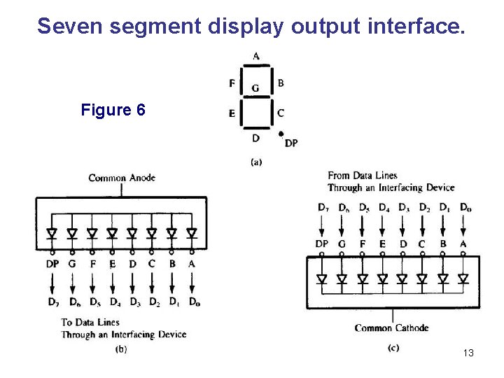
Seven segment display output interface. Figure 6 13

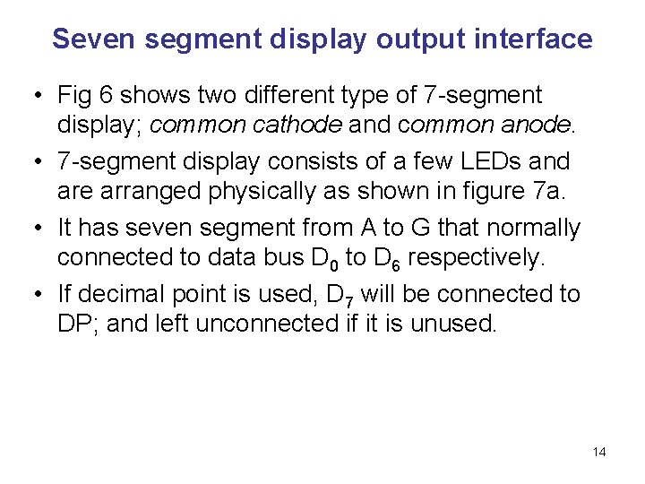
Seven segment display output interface • Fig 6 shows two different type of 7 -segment display; common cathode and common anode. • 7 -segment display consists of a few LEDs and are arranged physically as shown in figure 7 a. • It has seven segment from A to G that normally connected to data bus D 0 to D 6 respectively. • If decimal point is used, D 7 will be connected to DP; and left unconnected if it is unused. 14

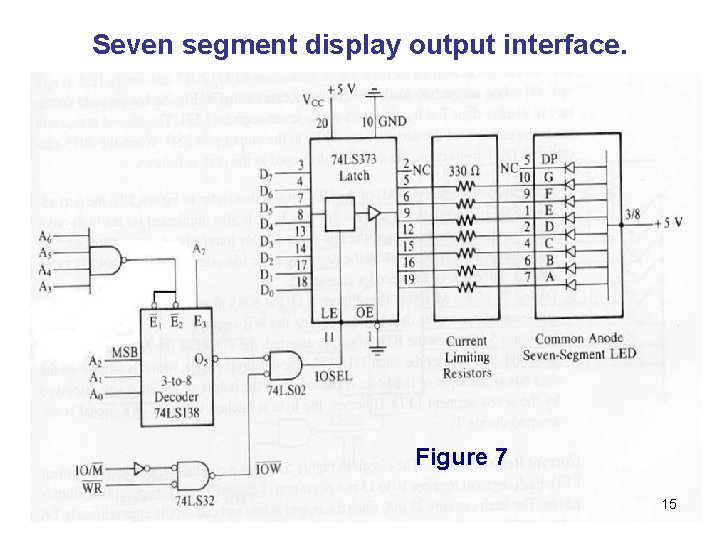
Seven segment display output interface. Figure 7 15

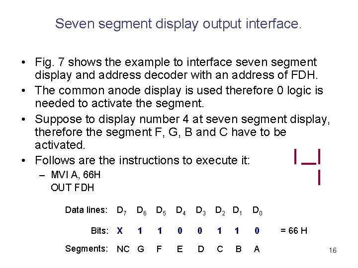
Seven segment display output interface. • Fig. 7 shows the example to interface seven segment display and address decoder with an address of FDH. • The common anode display is used therefore 0 logic is needed to activate the segment. • Suppose to display number 4 at seven segment display, therefore the segment F, G, B and C have to be activated. • Follows are the instructions to execute it: – MVI A, 66 H OUT FDH Data lines: D 7 D 6 D 5 D 4 D 3 D 2 D 1 D 0 1 1 0 NC G F E D C B A Bits: X Segments: = 66 H 16

Thank you Q&A 17