8085 Pin Diagram The 8085 A commonly known




- Slides: 11


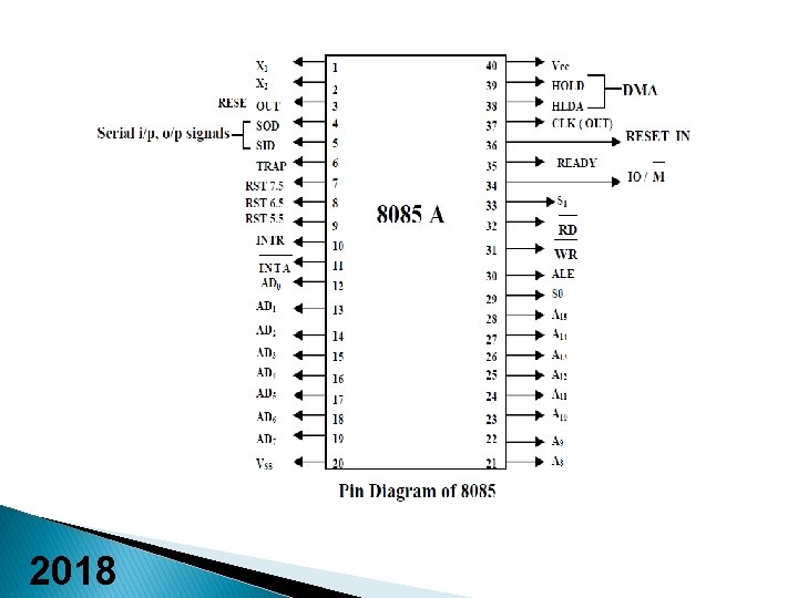
ﻛﻠﻴﺔ ﺍﻟﻬﻨﺪﺳﺔ / ﺟﺎﻣﻌﺔ ﺩﻳﺎﻟﻰ ﻗﺴﻢ ﺍﻟﻬﻨﺪﺳﺔ ﺍﻹﻟﻜﺘﺮﻭﻧﻴﺔ 8085 Pin Diagram The 8085 A (commonly known as the 8085) is an 8 bit general purpose microprocessor capable of addressing 64 K of memory. The device has forty pins, requires a +5 V single power supply, and can operate with a 3 MHz single phased clock. Figure 3 shows the logic pinout of the 8085 microprocessor. All the signals can be classified into six groups: 2018

ﻛﻠﻴﺔ ﺍﻟﻬﻨﺪﺳﺔ / ﺟﺎﻣﻌﺔ ﺩﻳﺎﻟﻰ ﻗﺴﻢ ﺍﻟﻬﻨﺪﺳﺔ ﺍﻹﻟﻜﺘﺮﻭﻧﻴﺔ 8085 Pin Diagram 1. Address bus. 2. Data bus. 3. Control and status signals. 4. Power supply and frequency signals. 5. Externally initiated signal. 6. Serial I/O. 2018

2018

ﻛﻠﻴﺔ ﺍﻟﻬﻨﺪﺳﺔ / ﺟﺎﻣﻌﺔ ﺩﻳﺎﻟﻰ ﻗﺴﻢ ﺍﻟﻬﻨﺪﺳﺔ ﺍﻹﻟﻜﺘﺮﻭﻧﻴﺔ 8085 Pin Diagram 1. ADDRESS BUS The 8085 has eight address lines A 15 – A 8, which are unidirectional and used as high order address bus. 2. MULTIPLEXED ADDRESS/DATA BUS The signals lines AD 7 AD 0 are bidirectional; they serve dual purpose. They are used as the low order address bus as well as the data bus. In executing an instruction, during the earlier part of the cycle, these lines are used as the low order address bus. During later part of die cycle, these lines are used as data bus. (This also known as multiplexing the bus. ) However, the low order address bus can be separated from these signals by using a latch. 2018

ﻛﻠﻴﺔ ﺍﻟﻬﻨﺪﺳﺔ / ﺟﺎﻣﻌﺔ ﺩﻳﺎﻟﻰ ﻗﺴﻢ ﺍﻟﻬﻨﺪﺳﺔ ﺍﻹﻟﻜﺘﺮﻭﻧﻴﺔ 8085 Pin Diagram 3. CONTROL AND STATUS SIGNALS This group of signals includes two control signals (RD and WR), three status signals IO/M, Si, and So) to identity the nature of the operation, and one special signal (ALE) to indicate the beginning of the operation. These signals are as follows: 4. ALE: Address Latch Enable: This is a positive going pulse generated every time the 8085 begins an operation (machine cycle); it indicates that the bits on AD 7 AD 0 are address bits. This signal is used primarily to latch the low order address from the multiplexed bus and generate a separate set of eight address lines, A 7 A 0. 2018

ﻛﻠﻴﺔ ﺍﻟﻬﻨﺪﺳﺔ / ﺟﺎﻣﻌﺔ ﺩﻳﺎﻟﻰ ﻗﺴﻢ ﺍﻟﻬﻨﺪﺳﺔ ﺍﻹﻟﻜﺘﺮﻭﻧﻴﺔ 8085 Pin Diagram 5. RD—Read: This is a Read control signal (active low). This signal indicates that the selected I/O or memory device is to be read and data are available on the data bus. 6. WR—Write: This is a Write control signal (active low). This signal indicates that the data on the data bus are to be written into a selected memory or I/O location. 2018

ﻛﻠﻴﺔ ﺍﻟﻬﻨﺪﺳﺔ / ﺟﺎﻣﻌﺔ ﺩﻳﺎﻟﻰ ﻗﺴﻢ ﺍﻟﻬﻨﺪﺳﺔ ﺍﻹﻟﻜﺘﺮﻭﻧﻴﺔ 8085 Pin Diagram 7. IO/M: This status signal used to differentiate between I/O and memory operations. When it is high, it indicates an I/O operation; when it is low, it indicates a memory operation. This signal is combined with RD (Read) and WR (Write) to generate I/O and memory control signals. . 8. S 0 and S 1: These status signals, similar to IO/M, can identify various operations but they are rarely used in small systems. All the operations and their associated status signals are listed in Table 3. 1 for reference. 2018

ﻛﻠﻴﺔ ﺍﻟﻬﻨﺪﺳﺔ / ﺟﺎﻣﻌﺔ ﺩﻳﺎﻟﻰ ﻗﺴﻢ ﺍﻟﻬﻨﺪﺳﺔ ﺍﻹﻟﻜﺘﺮﻭﻧﻴﺔ 8085 Pin Diagram POWER SUPPLY AND CLOCK FREQUENCY The power supply and frequency signals are as follows: • Vcc: +5 V power supply. • Vss: Ground Reference. • X 1, X 2: A crystal (or RC, LC network) is connected at these two pins. The frequency is internally divided by two: therefore, to operate a system at 3 MHz, the crystal, should have a frequency of 6 MHz. • CLK (OUT) Clock Output: This signal can be used as the system clock for other devices. 2018

ﻛﻠﻴﺔ ﺍﻟﻬﻨﺪﺳﺔ / ﺟﺎﻣﻌﺔ ﺩﻳﺎﻟﻰ ﻗﺴﻢ ﺍﻟﻬﻨﺪﺳﺔ ﺍﻹﻟﻜﺘﺮﻭﻧﻴﺔ Externally initiated signals, including interrupts The 8085 has five interrupt signals that can be used to interrupt a program execution. One of the signals. INTR (Interrupt Request), is identical to the 8080 A micro processor interrupt signal (INT); the others are enhancements to the 8080 A. The micro processoracknowledges an interrupt request by the INTA (Interrupt Acknowledge) signal. In addition to the interrupts, three pins—RESET. HOLD, and READY —accept the externally initiated signals as inputs. To respond to the HOLD request, it has one signal called HLDA (Hold Acknowledge). RESET IN: When the signal on this pin goes low, the program counter is set to zero, the buses are tri stated, and the MPU is reset. RESET OUT: This signal indicates that the MPU is being reset. The signal can be used to reset other devices. SERIAL I/O PORTS The 8085 has two signals to implement the serial transmission: SID (Serial Input Data) and SOD (Serial Output Data). 2018
