MICROPROCESSOR 8085 REFERENCE FUNDAMENTALS OF MICROPROCESSOR AND MICROCOMPUTERS
- Slides: 17

MICROPROCESSOR (8085) REFERENCE : FUNDAMENTALS OF MICROPROCESSOR AND MICROCOMPUTERS - B. RAM

INTRODUCTION TO 8085 MICROPROCESSOR Ø Microprocessor – central processing unit Ø Heart of the computer Ø 8085 is an 8 bit microprocessor Ø 40 pins Ø +5 vc power supply Ø 80 instructions, 246 opcodes

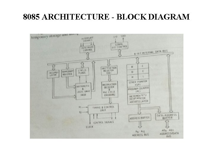
8085 ARCHITECTURE - BLOCK DIAGRAM

ARCHITECTURE Ø It has 3 main sections Ø ALU – Performs all arithmetic & logical operations Ø Timing & Control Unit – controls entire operations of microprocessor. Ø Registers Ø One 8 bit accumulator or Register A Ø Ø Ø Six 8 bit general purpose registers. B, C, D, E, H & L One 16 bit stack pointer, SP One 16 bit program counter, PC Instruction register Temporary register

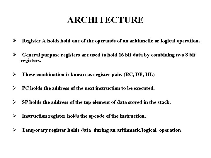
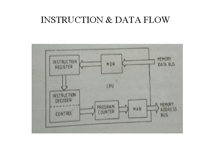
ARCHITECTURE Ø Register A holds hold one of the operands of an arithmetic or logical operation. Ø General purpose registers are used to hold 16 bit data by combining two 8 bit registers. Ø These combination is known as register pair. (BC, DE, HL) Ø PC holds the address of the next instruction to be executed. Ø SP holds the address of the top element of data stored in the stack. Ø Instruction register holds the opcode of the instruction. Ø Temporary register holds data during an arithmetic/logical operation

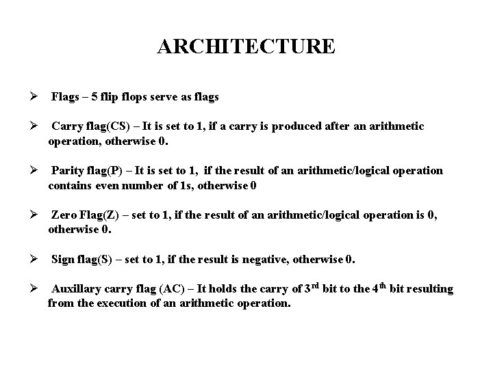
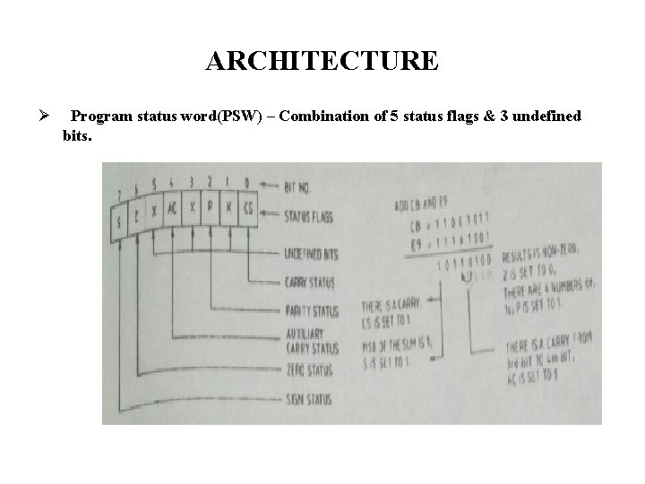
ARCHITECTURE Ø Flags – 5 flip flops serve as flags Ø Carry flag(CS) – It is set to 1, if a carry is produced after an arithmetic operation, otherwise 0. Ø Parity flag(P) – It is set to 1, if the result of an arithmetic/logical operation contains even number of 1 s, otherwise 0 Ø Zero Flag(Z) – set to 1, if the result of an arithmetic/logical operation is 0, otherwise 0. Ø Sign flag(S) – set to 1, if the result is negative, otherwise 0. Ø Auxillary carry flag (AC) – It holds the carry of 3 rd bit to the 4 th bit resulting from the execution of an arithmetic operation.

ARCHITECTURE Ø Program status word(PSW) – Combination of 5 status flags & 3 undefined bits.

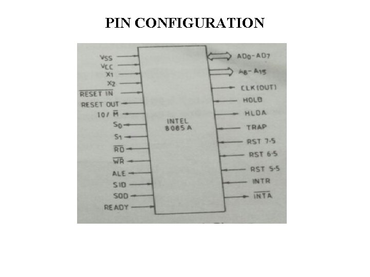
PIN CONFIGURATION

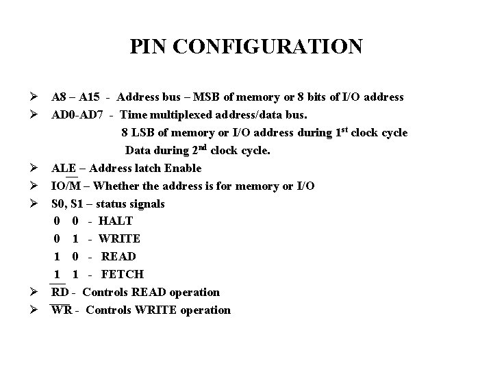
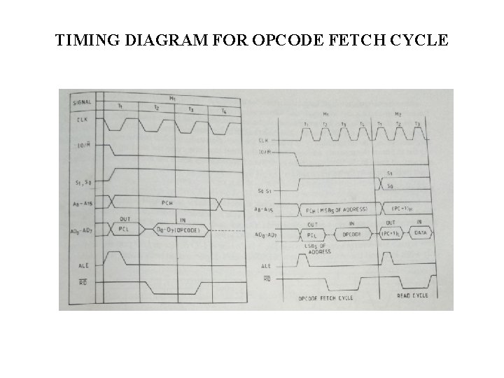
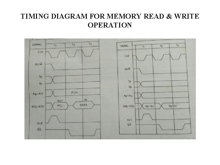
PIN CONFIGURATION Ø A 8 – A 15 - Address bus – MSB of memory or 8 bits of I/O address Ø AD 0 -AD 7 - Time multiplexed address/data bus. 8 LSB of memory or I/O address during 1 st clock cycle Data during 2 nd clock cycle. Ø ALE – Address latch Enable Ø IO/M – Whether the address is for memory or I/O Ø S 0, S 1 – status signals 0 0 - HALT 0 1 - WRITE 1 0 - READ 1 1 - FETCH Ø RD - Controls READ operation Ø WR - Controls WRITE operation

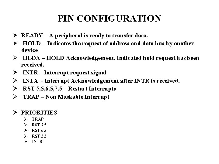
PIN CONFIGURATION Ø READY – A peripheral is ready to transfer data. Ø HOLD - Indicates the request of address and data bus by another device Ø HLDA – HOLD Acknowledgement. Indicated hold request has been received. Ø INTR – Interrupt request signal Ø INTA - Interrupt Acknowledgement after INTR is received. Ø RST 5. 5, 6. 5, 7. 5 – Restart Interrupts Ø TRAP – Non Maskable Interrupt Ø PRIORITIES Ø Ø Ø TRAP RST 7. 5 RST 6. 5 RST 5. 5 INTR

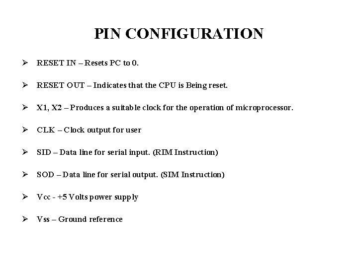
PIN CONFIGURATION Ø RESET IN – Resets PC to 0. Ø RESET OUT – Indicates that the CPU is Being reset. Ø X 1, X 2 – Produces a suitable clock for the operation of microprocessor. Ø CLK – Clock output for user Ø SID – Data line for serial input. (RIM Instruction) Ø SOD – Data line for serial output. (SIM Instruction) Ø Vcc - +5 Volts power supply Ø Vss – Ground reference

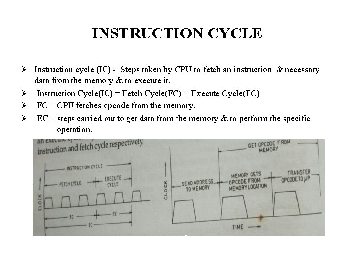
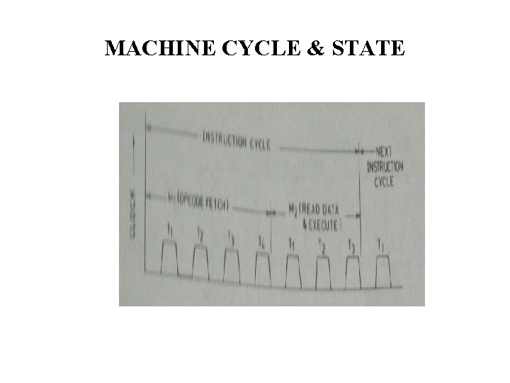
INSTRUCTION CYCLE Ø Instruction cycle (IC) - Steps taken by CPU to fetch an instruction & necessary data from the memory & to execute it. Ø Instruction Cycle(IC) = Fetch Cycle(FC) + Execute Cycle(EC) Ø FC – CPU fetches opcode from the memory. Ø EC – steps carried out to get data from the memory & to perform the specific operation.

MACHINE CYCLE & STATE

INSTRUCTION & DATA FLOW

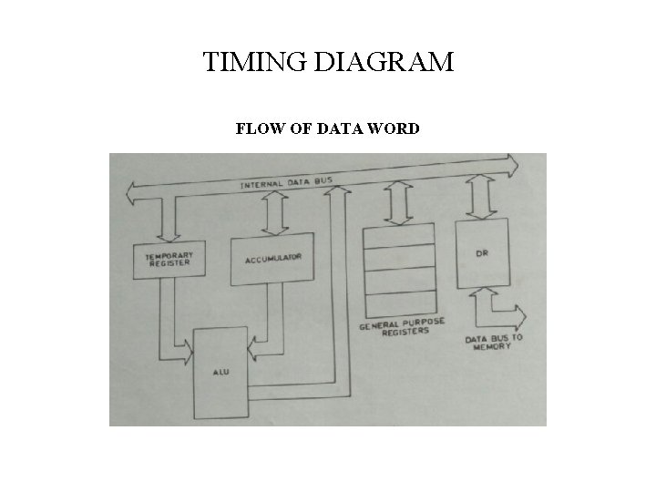
TIMING DIAGRAM FLOW OF DATA WORD

TIMING DIAGRAM FOR OPCODE FETCH CYCLE

TIMING DIAGRAM FOR MEMORY READ & WRITE OPERATION