Microprocessor Design Nestoras Evmorfopoulos Microprocessor Design Outline l
- Slides: 87

Microprocessor Design Nestoras Evmorfopoulos Microprocessor Design

Outline l l l l VLSI design flow Top-down (standard-cell) design Bottom-up (full-custom) design Layout or physical-level design Placement I/O and P/G pads Routing Power distribution Clock distribution Design Rules Checking - DRC Layout Versus Schematic - LVS Parasitic extraction Post-layout timing analysis Power analysis 3/8/2021 Microprocessor Design 2

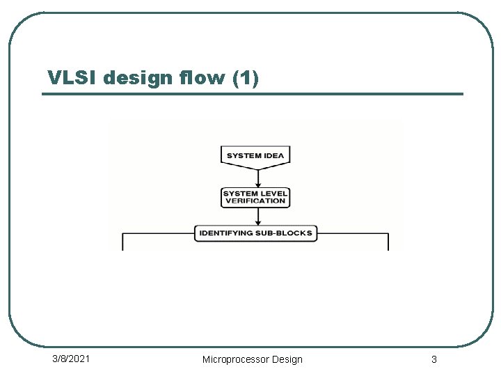
VLSI design flow (1) 3/8/2021 Microprocessor Design 3

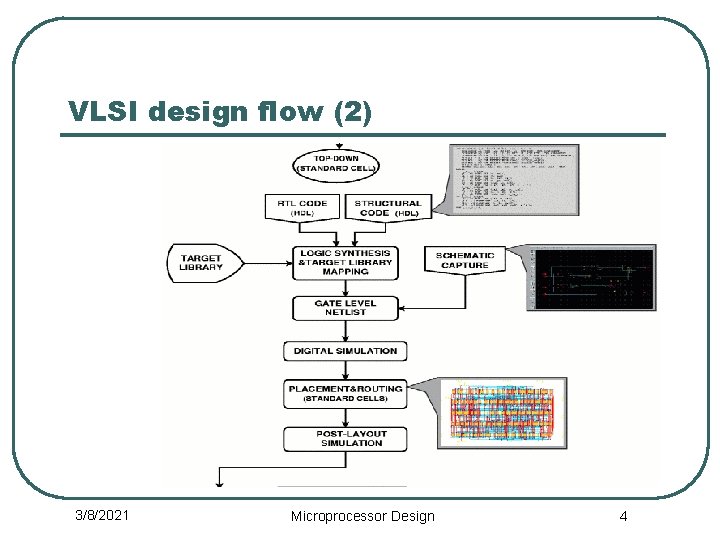
VLSI design flow (2) 3/8/2021 Microprocessor Design 4

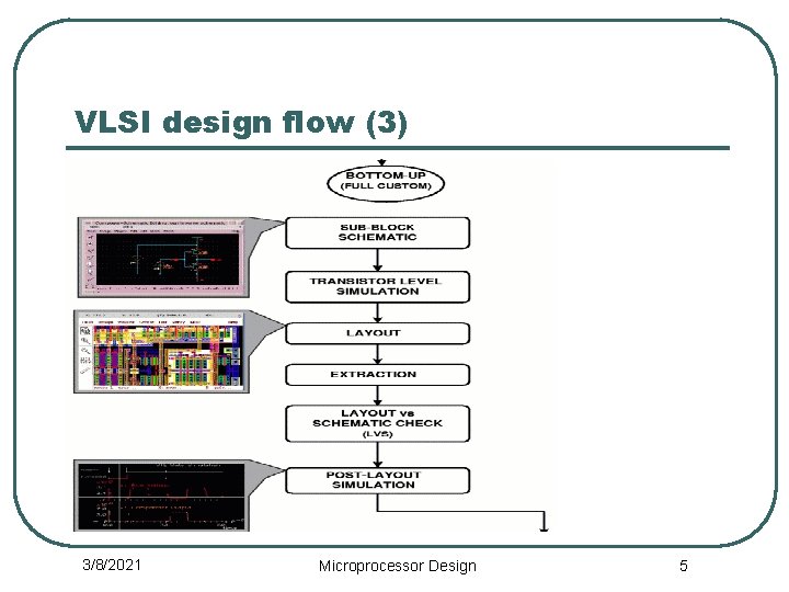
VLSI design flow (3) 3/8/2021 Microprocessor Design 5

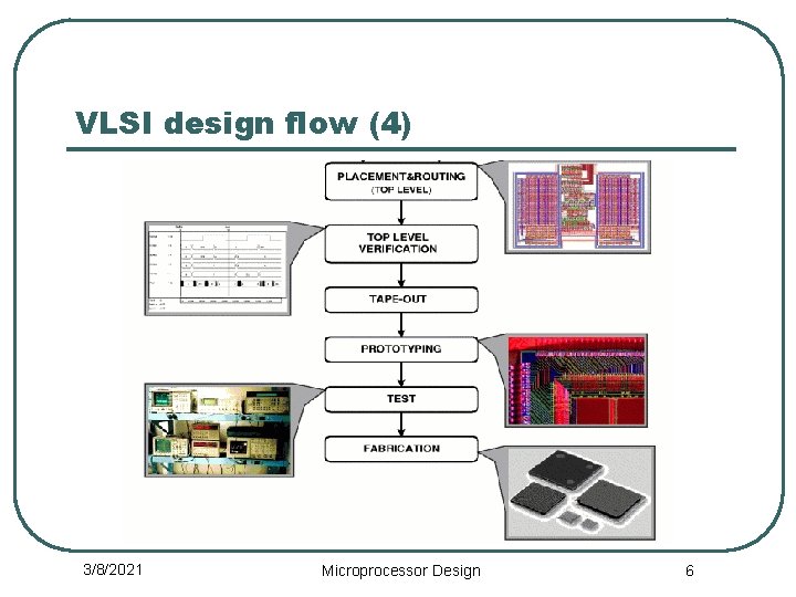
VLSI design flow (4) 3/8/2021 Microprocessor Design 6

Top-down (standard-cell) design l l Describe design in RTL form using a Hardware Description Language (like VHDL) Synthesize HDL code into gate-level design using a logic synthesis tool (e. g. Design Compiler) • Synthesis performed in conjunction with a library of existing standard cells (gates and latches) l Perform functional simulation of the design l Flow appropriate for low-end systems like FPGA implementations or small custom Application-Specific Integrated Circuits (ASICs) 3/8/2021 Microprocessor Design 7

Bottom-up (full-custom) design l Design straight at the transistor level • • l l l Develop high-performance cells like dynamic CMOS gates (domino logic, NP logic, cascode voltage switch logic - CVSL, etc. ) and custom latches Apply universal transistor sizing Perform electrical (transistor-level) simulation (e. g. SPICE) Perform custom (physical-level) layout of the developed cells (with known techniques) Flow appropriate for high-end systems like microprocessors 3/8/2021 Microprocessor Design 8

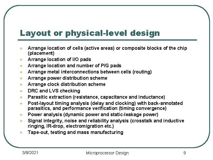
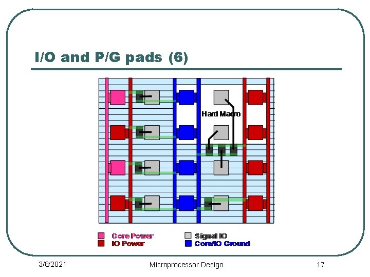
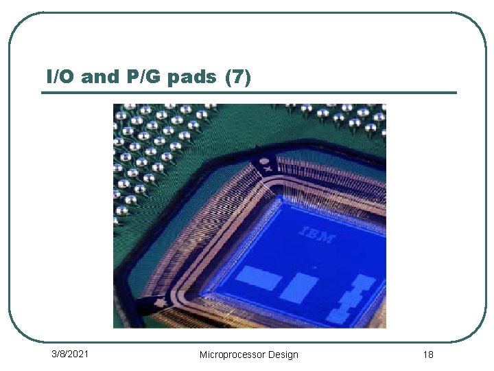
Layout or physical-level design l l l Arrange location of cells (active areas) or composite blocks of the chip (placement) Arrange location of I/O pads Arrange location and number of P/G pads Arrange metal interconnections between cells (routing) Arrange power distribution scheme Arrange clock distribution scheme DRC and LVS checking Parasitic extraction (resistance, capacitance and inductance) Post-layout timing analysis (delay and clocking) with back-annotated parasitics, and performance verification (timing convergence) Power analysis (dynamic power and static-leakage power) Signal integrity, noise and reliability analysis (crosstalk and inductive ringing, IR-drop, electromigration etc. ) Tape-out, testing and mass manufacturing 3/8/2021 Microprocessor Design 9

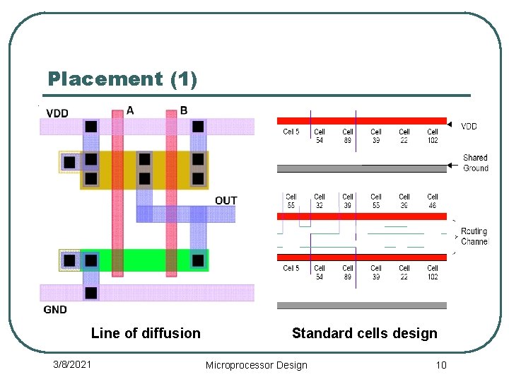
Placement (1) Line of diffusion 3/8/2021 Standard cells design Microprocessor Design 10

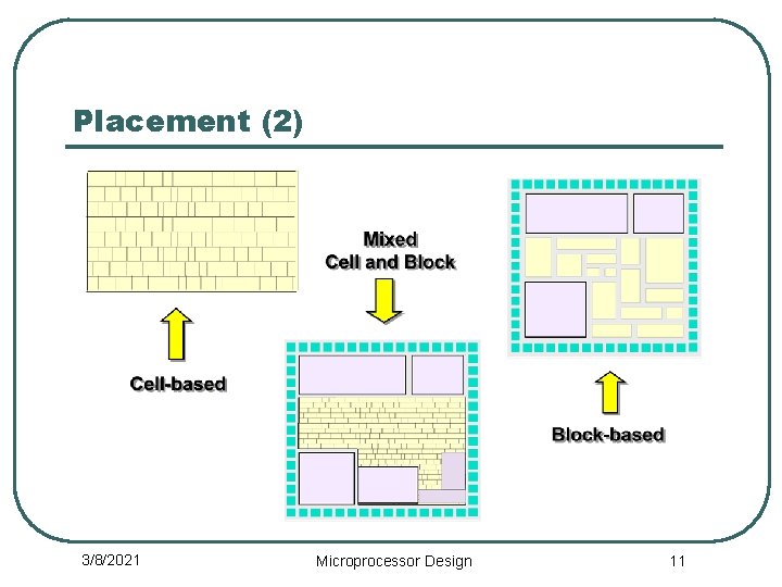
Placement (2) 3/8/2021 Microprocessor Design 11

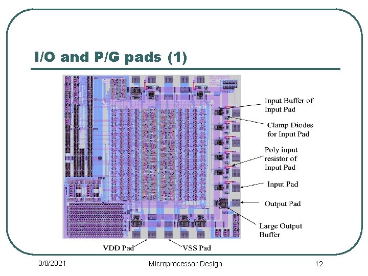
I/O and P/G pads (1) 3/8/2021 Microprocessor Design 12

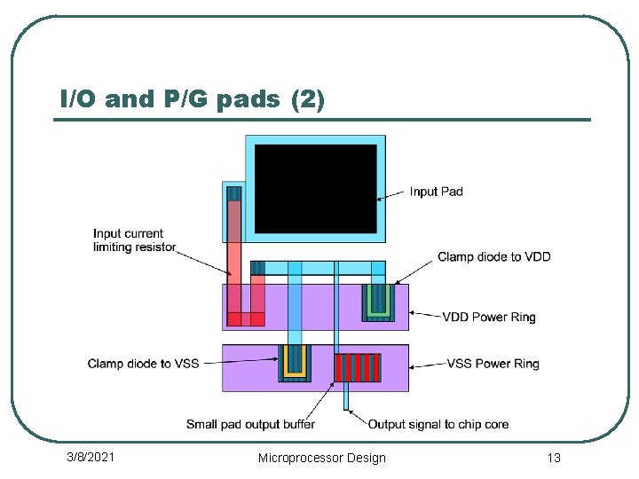
I/O and P/G pads (2) 3/8/2021 Microprocessor Design 13

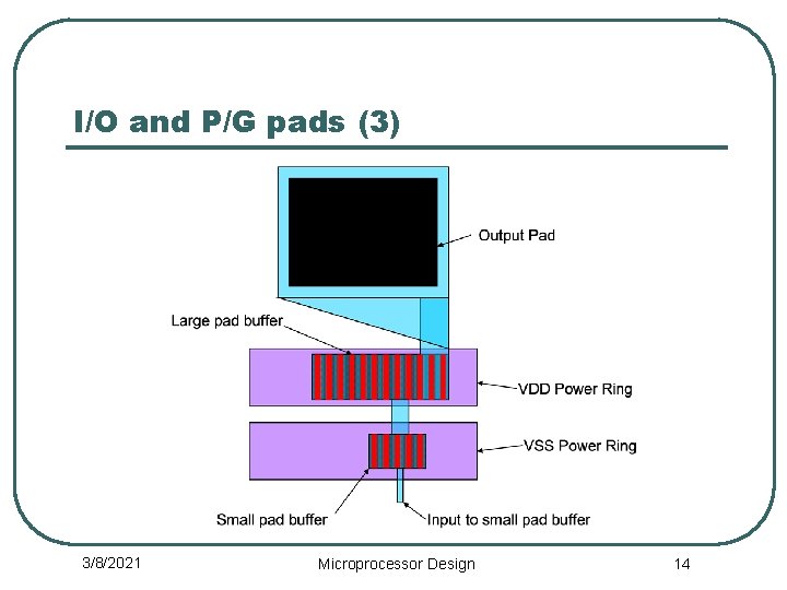
I/O and P/G pads (3) 3/8/2021 Microprocessor Design 14

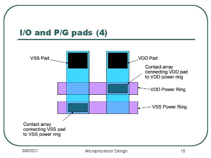
I/O and P/G pads (4) 3/8/2021 Microprocessor Design 15

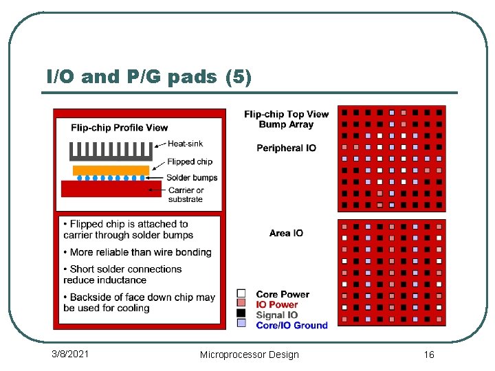
I/O and P/G pads (5) 3/8/2021 Microprocessor Design 16

I/O and P/G pads (6) 3/8/2021 Microprocessor Design 17

I/O and P/G pads (7) 3/8/2021 Microprocessor Design 18

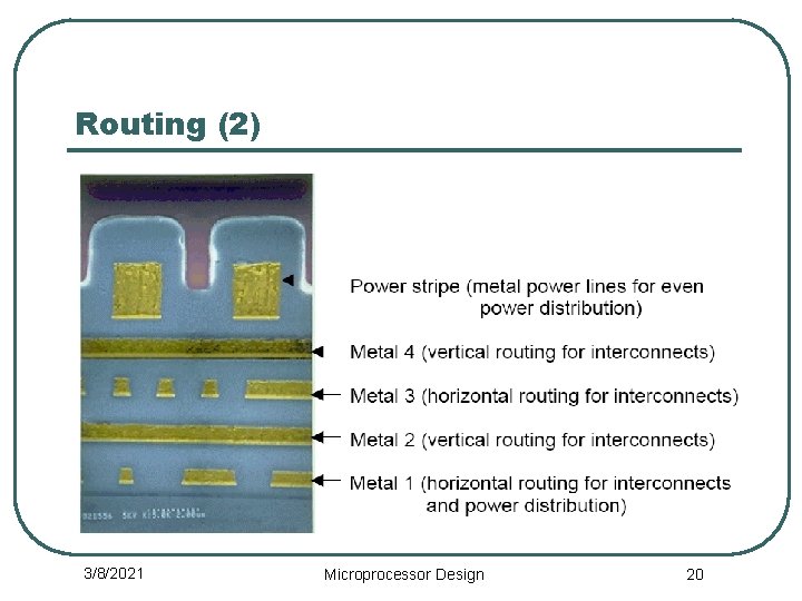
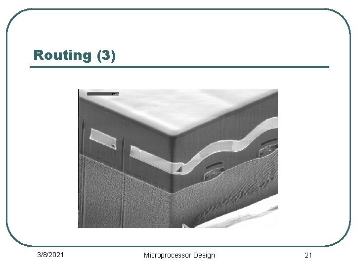
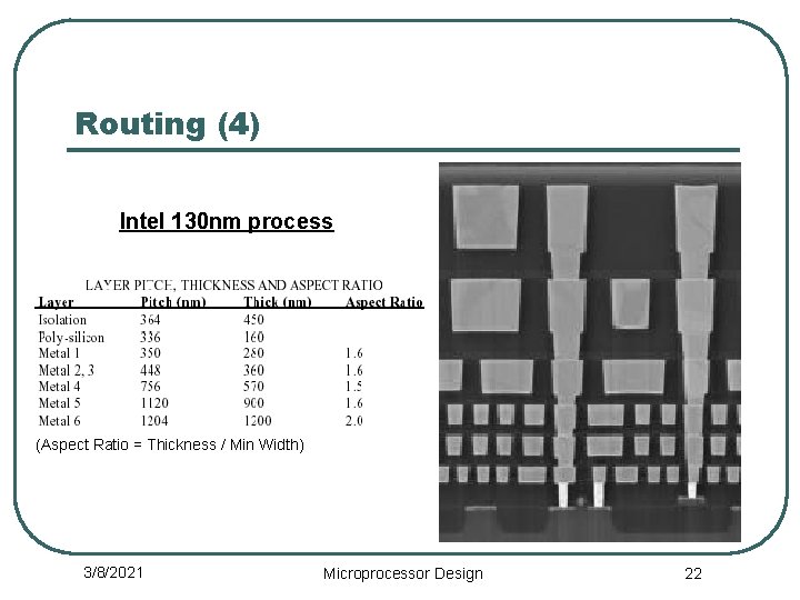
Routing (1) l l l Capability of 8+ metal layers in contemporary technologies Automatic tools use each metal layer to perform routing in one direction only (horizontal or vertical) Upper metal layers become more and more uneven, and thus lines must be designed wider with greater pitches • l => upper layers are less resistive and the top layer is used for critical routing such as power/clock lines and global signals Most recent developments in routing technology: • • Copper (Cu) instead of Aluminum (Al) interconnects offer lower resistance and higher propagation speed (as well as greater strength against the electromigration phenomenon) Low-k dielectrics (with dielectric constant ε < 4 of Si. O 2) as means of isolation between the metal layers offer reduced interconnect capacitance 3/8/2021 Microprocessor Design 19

Routing (2) 3/8/2021 Microprocessor Design 20

Routing (3) 3/8/2021 Microprocessor Design 21

Routing (4) Intel 130 nm process (Aspect Ratio = Thickness / Min Width) 3/8/2021 Microprocessor Design 22

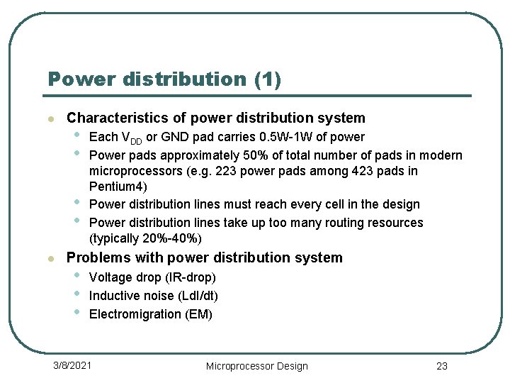
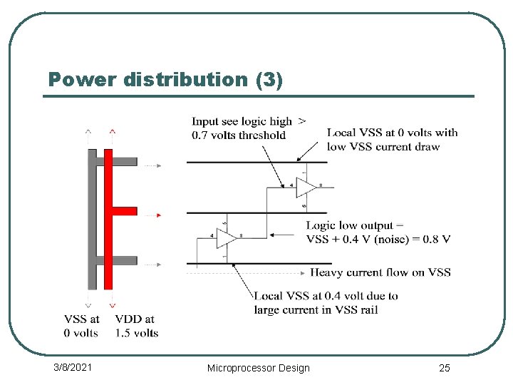
Power distribution (1) l Characteristics of power distribution system • • l Each VDD or GND pad carries 0. 5 W-1 W of power Power pads approximately 50% of total number of pads in modern microprocessors (e. g. 223 power pads among 423 pads in Pentium 4) Power distribution lines must reach every cell in the design Power distribution lines take up too many routing resources (typically 20%-40%) Problems with power distribution system • • • Voltage drop (IR-drop) Inductive noise (Ld. I/dt) Electromigration (EM) 3/8/2021 Microprocessor Design 23

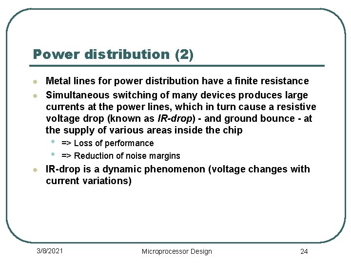
Power distribution (2) l l Metal lines for power distribution have a finite resistance Simultaneous switching of many devices produces large currents at the power lines, which in turn cause a resistive voltage drop (known as IR-drop) - and ground bounce - at the supply of various areas inside the chip • • l => Loss of performance => Reduction of noise margins IR-drop is a dynamic phenomenon (voltage changes with current variations) 3/8/2021 Microprocessor Design 24

Power distribution (3) 3/8/2021 Microprocessor Design 25

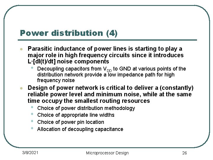
Power distribution (4) l Parasitic inductance of power lines is starting to play a major role in high frequency circuits since it introduces L∙[d. I(t)/dt] noise components • l Decoupling capacitors from VDD to GND at various points of the distribution network provide a low impedance path for high frequency noise Design of power network is critical to deliver a (constantly) reliable power level and minimum noise, while at the same time occupy the smallest routing resources • • Choice of power distribution methodology Choice of appropriate line widths Choice of power pin location Allocation of decoupling capacitance 3/8/2021 Microprocessor Design 26

Power distribution (5) 3/8/2021 Microprocessor Design 27

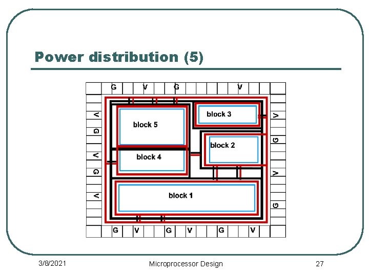
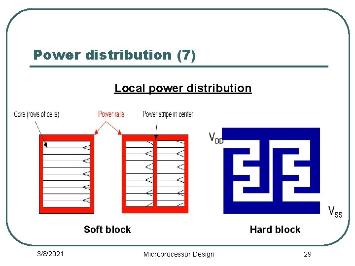
Power distribution (6) l l Advantages of rings methodology • • • Occupies a small portion of available routing area Rings and lines can be shared between blocks Easy to insert hard blocks with their own internal power structure Disadvantages of rings methodology • • Non regular structure requiring more detailed IR-drop (and EM) analysis Power structure tailored to the demands of each block => changes in design are likely to change power structure 3/8/2021 Microprocessor Design 28

Power distribution (7) Local power distribution Soft block 3/8/2021 Hard block Microprocessor Design 29

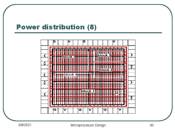
Power distribution (8) 3/8/2021 Microprocessor Design 30

Power distribution (9) l Advantages of grid methodology • • l Regular structure giving rise to straightforward IR-drop (and EM) calculations Path redundancy allows less sensitivity to current variations Ready local power distribution for standard cells within soft blocks Changes in design do not affect power structure Disadvantages of grid methodology • • • Takes up significant routing resources Not easy to accommodate hard blocks with existing power structure (must lie at lower metal layers and be interfaced with stacks of vias) Grid structure for cells within soft blocks is usually not necessary 3/8/2021 Microprocessor Design 31

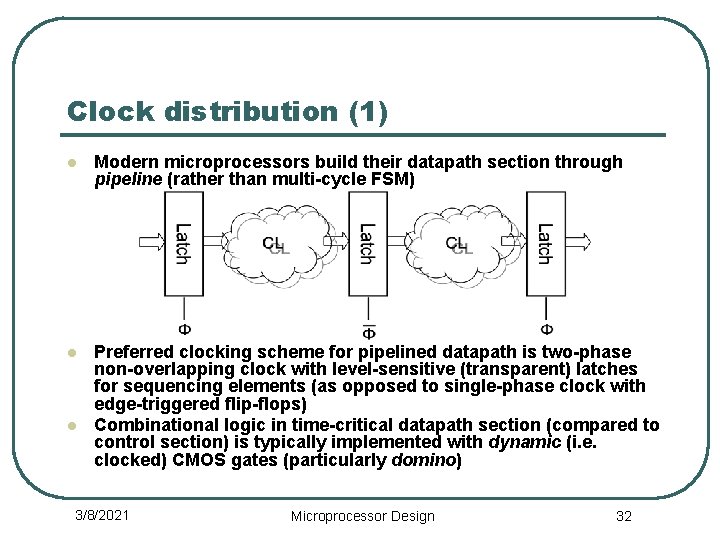
Clock distribution (1) l Modern microprocessors build their datapath section through pipeline (rather than multi-cycle FSM) l Preferred clocking scheme for pipelined datapath is two-phase non-overlapping clock with level-sensitive (transparent) latches for sequencing elements (as opposed to single-phase clock with edge-triggered flip-flops) Combinational logic in time-critical datapath section (compared to control section) is typically implemented with dynamic (i. e. clocked) CMOS gates (particularly domino) l 3/8/2021 Microprocessor Design 32

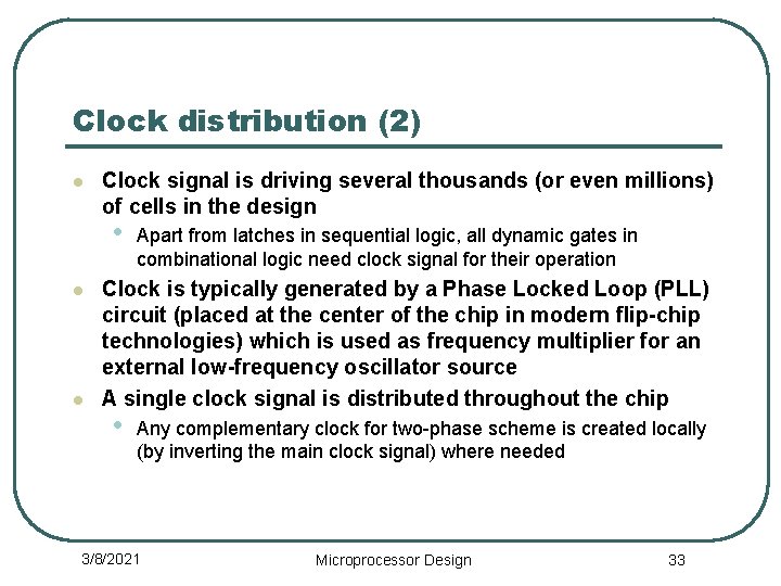
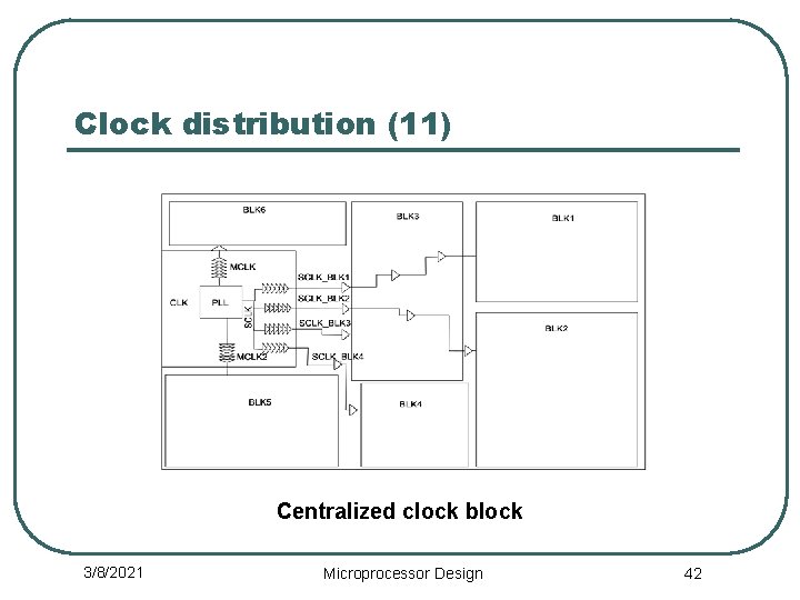
Clock distribution (2) l Clock signal is driving several thousands (or even millions) of cells in the design • l l Apart from latches in sequential logic, all dynamic gates in combinational logic need clock signal for their operation Clock is typically generated by a Phase Locked Loop (PLL) circuit (placed at the center of the chip in modern flip-chip technologies) which is used as frequency multiplier for an external low-frequency oscillator source A single clock signal is distributed throughout the chip • Any complementary clock for two-phase scheme is created locally (by inverting the main clock signal) where needed 3/8/2021 Microprocessor Design 33

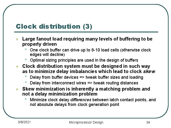
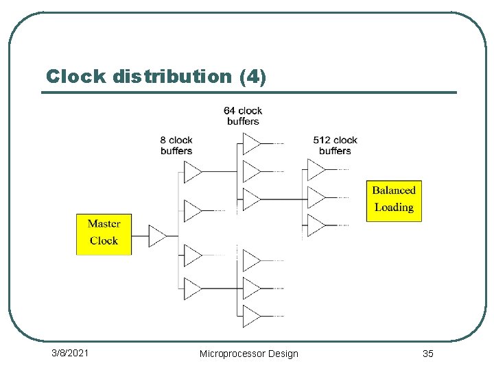
Clock distribution (3) l Large fanout load requiring many levels of buffering to be properly driven • • l Clock distribution system must be designed in such way as to minimize delay imbalancies which lead to clock skew • • l One clock buffer can drive up to 8 -10 load cells (otherwise clock edges will decline) Optimal sizing principles are used in the design of buffers Delay from buffer devices => tweak buffer sizes and loading Delay from interconnect wires => tweak routing distances Skew minimization is inherently a matching problem and not a delay minimization problem • Minimize clock delay differences between latch contact points, and not absolute delays from clock generation point 3/8/2021 Microprocessor Design 34

Clock distribution (4) 3/8/2021 Microprocessor Design 35

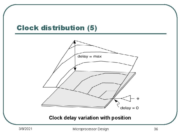
Clock distribution (5) Clock delay variation with position 3/8/2021 Microprocessor Design 36

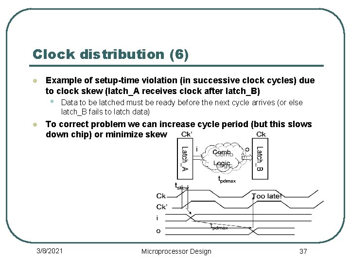
Clock distribution (6) l Example of setup-time violation (in successive clock cycles) due to clock skew (latch_A receives clock after latch_B) • l Data to be latched must be ready before the next cycle arrives (or else latch_B fails to latch data) To correct problem we can increase cycle period (but this slows down chip) or minimize skew 3/8/2021 Microprocessor Design 37

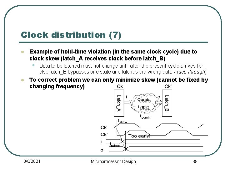
Clock distribution (7) l Example of hold-time violation (in the same clock cycle) due to clock skew (latch_A receives clock before latch_B) • l Data to be latched must not change until after the present cycle arrives (or else latch_B bypasses one state and latches the wrong data - race through) To correct problem we can only minimize skew (cannot be fixed by changing frequency) 3/8/2021 Microprocessor Design 38

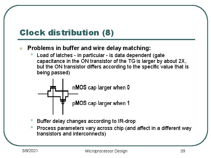
Clock distribution (8) l Problems in buffer and wire delay matching: • Load of latches - in particular - is data dependent (gate capacitance in the ON transistor of the TG is larger by about 2 X, but the ON transistor differs according to the specific value that is being passed) • • Buffer delay changes according to IR-drop Process parameters vary across chip (and affect in a different way transistors and interconnects) 3/8/2021 Microprocessor Design 39

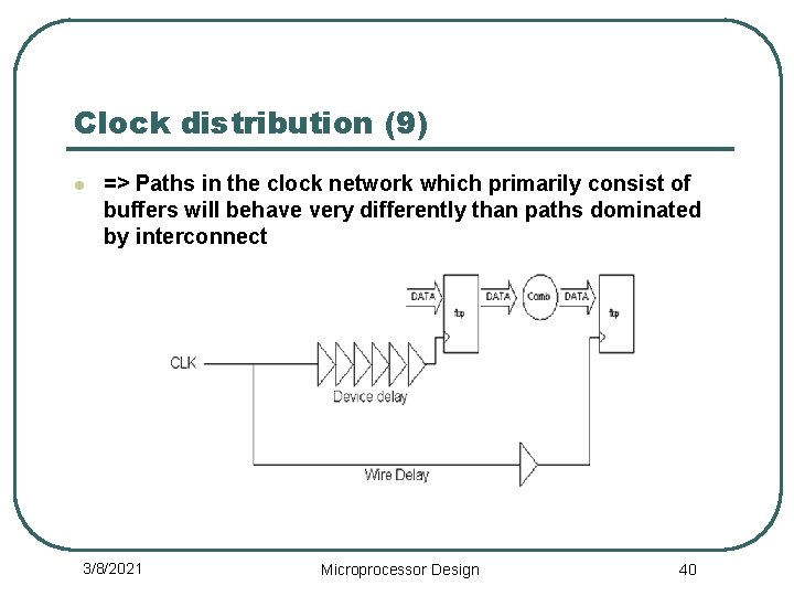
Clock distribution (9) l => Paths in the clock network which primarily consist of buffers will behave very differently than paths dominated by interconnect 3/8/2021 Microprocessor Design 40

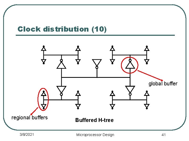
Clock distribution (10) global buffer regional buffers 3/8/2021 Buffered H-tree Microprocessor Design 41

Clock distribution (11) Centralized clock block 3/8/2021 Microprocessor Design 42

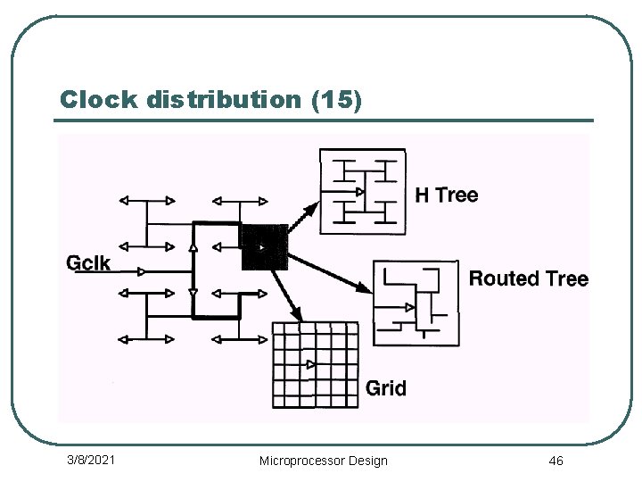
Clock distribution (12) l Advantages of buffered H-trees • • • l Small occupation of routing resources (both in buffering and wiring) Low power dissipation of the network itself (due to small wiring capacitance and small number of buffers) Ability to gate clocks to reduce power even further Disadvantages of buffered H-trees • • Fairly difficult design for delay balancing Not easily adaptable to changes in the design and clock loading 3/8/2021 Microprocessor Design 43

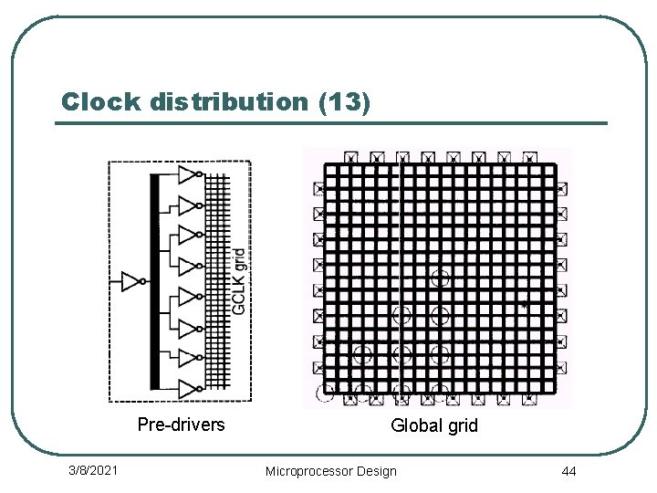
Clock distribution (13) Pre-drivers 3/8/2021 Global grid Microprocessor Design 44

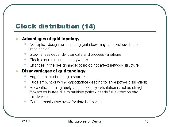
Clock distribution (14) l Advantages of grid topology • • l No explicit design for matching (but skew may still exist due to load imbalancies) Skew is less dependent on data and process variations Clock signals available everywhere Changes in the design and loading do not affect network structure Disadvantages of grid topology • • Huge amount of routing resources Huge amount of wiring capacitance (leading to large power dissipation) More difficult timing analysis (clock delay calculation is not as straightforward as in tree due to multiple paths - needs full extraction and simulation) Cannot manipulate skew for time borrowing 3/8/2021 Microprocessor Design 45

Clock distribution (15) 3/8/2021 Microprocessor Design 46

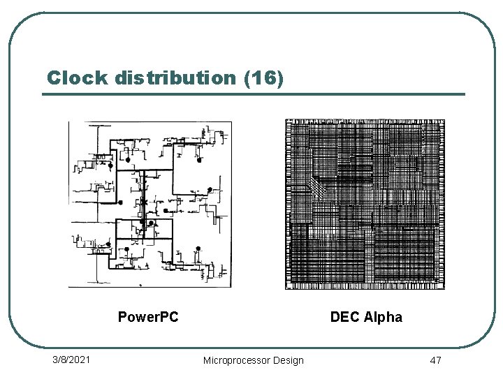
Clock distribution (16) Power. PC 3/8/2021 DEC Alpha Microprocessor Design 47

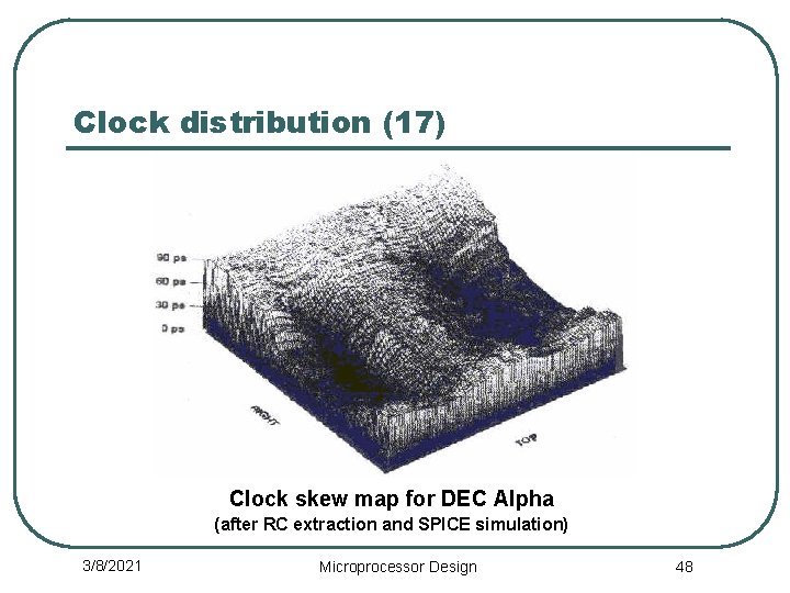
Clock distribution (17) Clock skew map for DEC Alpha (after RC extraction and SPICE simulation) 3/8/2021 Microprocessor Design 48

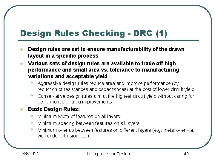
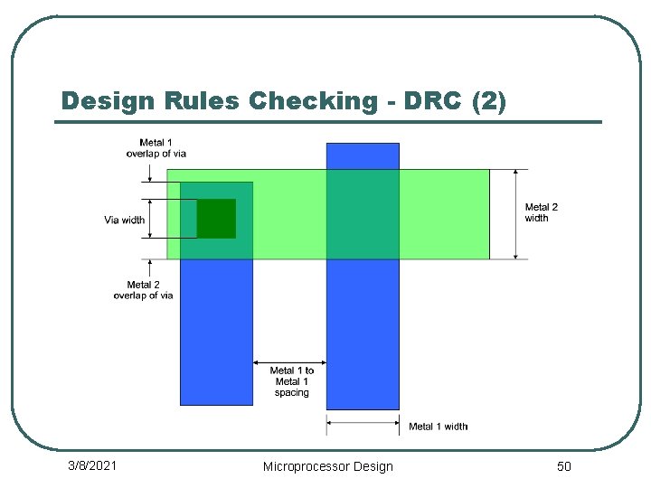
Design Rules Checking - DRC (1) l l Design rules are set to ensure manufacturability of the drawn layout in a specific process Various sets of design rules are available to trade off high performance and small area vs. tolerance to manufacturing variations and acceptable yield • • l Aggressive design rules reduce area and improve performance (by reduction of resistances and capacitances) at the cost of lower circuit yield Conservative design rules aim at the highest circuit yield without caring for performance or area improvements Basic Design Rules: • • • Minimum width of features on all layers Minimum spacing between features on all layers Minimum overlap between features on different layers (e. g. metal over via, well under diffusion etc. ) 3/8/2021 Microprocessor Design 49

Design Rules Checking - DRC (2) 3/8/2021 Microprocessor Design 50

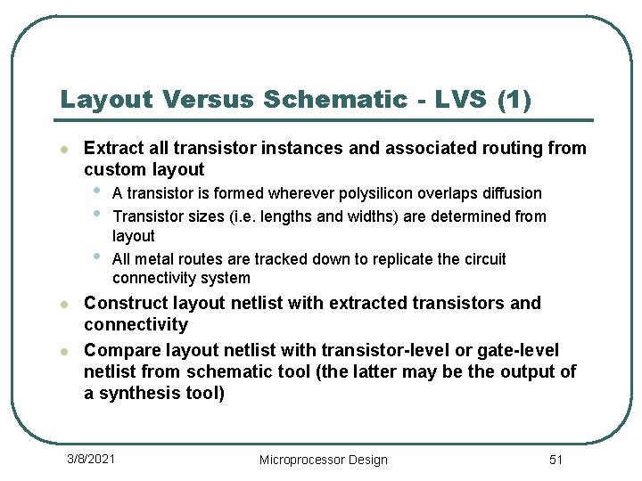
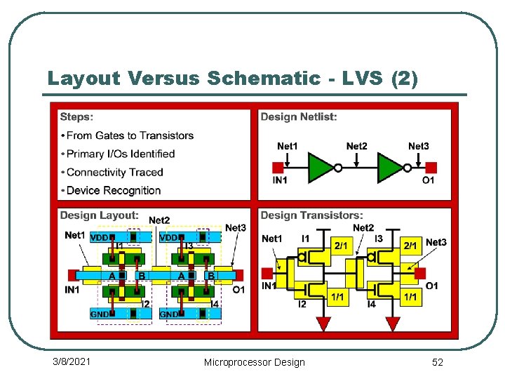
Layout Versus Schematic - LVS (1) l Extract all transistor instances and associated routing from custom layout • • • l l A transistor is formed wherever polysilicon overlaps diffusion Transistor sizes (i. e. lengths and widths) are determined from layout All metal routes are tracked down to replicate the circuit connectivity system Construct layout netlist with extracted transistors and connectivity Compare layout netlist with transistor-level or gate-level netlist from schematic tool (the latter may be the output of a synthesis tool) 3/8/2021 Microprocessor Design 51

Layout Versus Schematic - LVS (2) 3/8/2021 Microprocessor Design 52

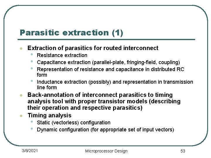
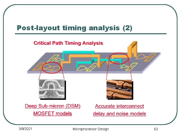
Parasitic extraction (1) l Extraction of parasitics for routed interconnect • • l l Resistance extraction Capacitance extraction (parallel-plate, fringing-field, coupling) Representation of resistance and capacitance in distributed RC form Inductance extraction (possibly) and representation in transmission line form Back-annotation of interconnect parasitics to timing analysis tool with proper transistor models (describing their operation and respective parasitics) Timing analysis • • Static (vectorless) configuration Dynamic configuration (for appropriate set of input vectors) 3/8/2021 Microprocessor Design 53

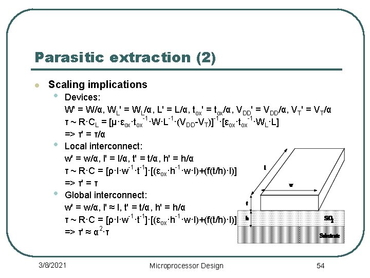
Parasitic extraction (2) l Scaling implications • • • Devices: W' = W/α, WL' = WL/α, L' = L/α, tox' = tox/α, VDD' = VDD/α, VT' = VT/α τ ~ R·CL = [μ·εox·tox-1·W·L-1·(VDD-VT)]-1·[εox·tox-1·WL·L] => τ' = τ/α Local interconnect: w' = w/α, l' = l/α, t' = t/α, h' = h/α τ ~ R·C = [ρ·l·w-1·t-1]·[(εox·h-1·w·l)+(f(t/h)·l)] => τ' = τ Global interconnect: w' = w/α, l' ≈ l, t' = t/α, h' = h/α τ ~ R·C = [ρ·l·w-1·t-1]·[(εox·h-1·w·l)+(f(t/h)·l)] => τ' ≈ α 2·τ 3/8/2021 Microprocessor Design 54

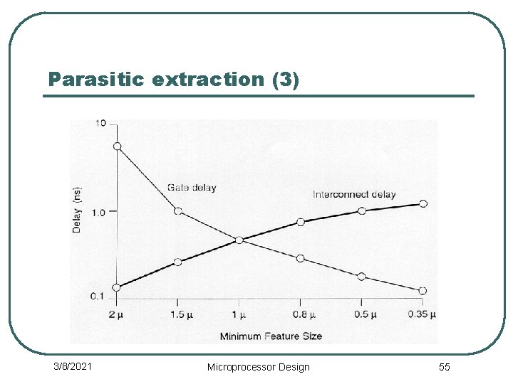
Parasitic extraction (3) 3/8/2021 Microprocessor Design 55

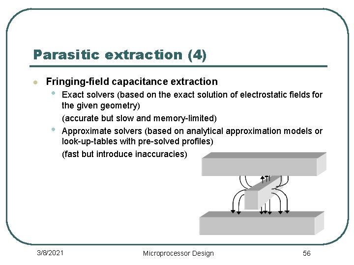
Parasitic extraction (4) l Fringing-field capacitance extraction • • Exact solvers (based on the exact solution of electrostatic fields for the given geometry) (accurate but slow and memory-limited) Approximate solvers (based on analytical approximation models or look-up-tables with pre-solved profiles) (fast but introduce inaccuracies) 3/8/2021 Microprocessor Design 56

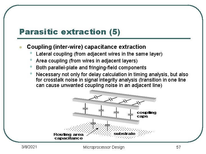
Parasitic extraction (5) l Coupling (inter-wire) capacitance extraction • • Lateral coupling (from adjacent wires in the same layer) Area coupling (from wires in adjacent layers) Both parallel-plate and fringing-field components Necessary not only for delay calculation in timing analysis, but also for crosstalk noise in signal integrity analysis (transition in one line can cause unwanted coupling noise in an adjacent line) 3/8/2021 Microprocessor Design 57

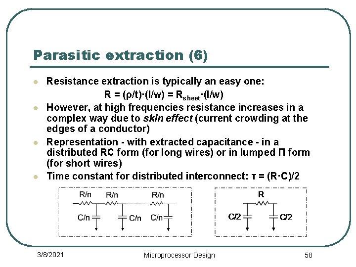
Parasitic extraction (6) l l Resistance extraction is typically an easy one: R = (ρ/t)·(l/w) = Rsheet·(l/w) However, at high frequencies resistance increases in a complex way due to skin effect (current crowding at the edges of a conductor) Representation - with extracted capacitance - in a distributed RC form (for long wires) or in lumped Π form (for short wires) Time constant for distributed interconnect: τ = (R·C)/2 3/8/2021 Microprocessor Design 58

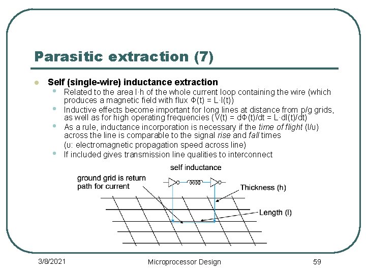
Parasitic extraction (7) l Self (single-wire) inductance extraction • • Related to the area l·h of the whole current loop containing the wire (which produces a magnetic field with flux Φ(t) = L·I(t)) Inductive effects become important for long lines at distance from p/g grids, as well as for high operating frequencies (V(t) = dΦ(t)/dt = L·d. I(t)/dt) As a rule, inductance incorporation is necessary if the time of flight (l/υ) across the line is comparable to the signal rise and fall times (υ: electromagnetic propagation speed across line) If included gives transmission line qualities to interconnect 3/8/2021 Microprocessor Design 59

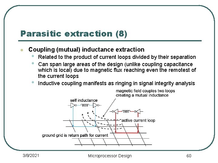
Parasitic extraction (8) l Coupling (mutual) inductance extraction • • • Related to the product of current loops divided by their separation Can span large areas of the design (unlike coupling capacitance which is local) due to magnetic flux reaching even the remotest of the current loops Inductive coupling manifests as ringing in signal integrity analysis 3/8/2021 Microprocessor Design 60

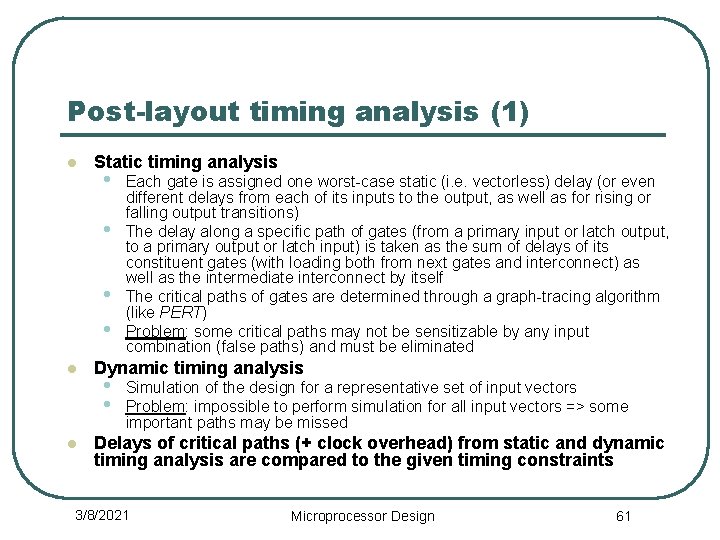
Post-layout timing analysis (1) l Static timing analysis • • l l Each gate is assigned one worst-case static (i. e. vectorless) delay (or even different delays from each of its inputs to the output, as well as for rising or falling output transitions) The delay along a specific path of gates (from a primary input or latch output, to a primary output or latch input) is taken as the sum of delays of its constituent gates (with loading both from next gates and interconnect) as well as the intermediate interconnect by itself The critical paths of gates are determined through a graph-tracing algorithm (like PERT) Problem: some critical paths may not be sensitizable by any input combination (false paths) and must be eliminated Dynamic timing analysis • • Simulation of the design for a representative set of input vectors Problem: impossible to perform simulation for all input vectors => some important paths may be missed Delays of critical paths (+ clock overhead) from static and dynamic timing analysis are compared to the given timing constraints 3/8/2021 Microprocessor Design 61

Post-layout timing analysis (2) 3/8/2021 Microprocessor Design 62

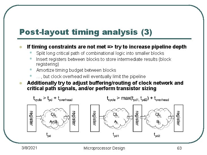
Post-layout timing analysis (3) l If timing constraints are not met => try to increase pipeline depth • • l Split long critical path of combinational logic into smaller blocks Insert registers between blocks to store intermediate results (block registering) Amortize timing budget between blocks …, but clock overhead will eventually limit the pipeline Additionally try to adjust buffering/routing of clock network and critical path signals, and/or perform transistor sizing 3/8/2021 Microprocessor Design 63

Post-layout timing analysis (4) 3/8/2021 Microprocessor Design 64

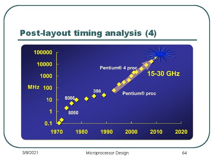
Post-layout timing analysis (5) l ~2 X frequency increase with each new generation • • l Half (i. e. ~1. 5 X) from advanced process technology (scaling is performed by 1/α ≈ 1/1. 5 ≈ 0. 7) Other half (1. 5 X) by increasing pipeline depth Examples: • • Pentium (0. 35μm) at 200 MHz vs. Pentium-II (0. 35μm) at 300 MHz => 1. 5 X difference due to increased pipeline depth Pentium-II (0. 35μm) at 300 MHz vs. Pentium-III (0. 25μm) at 600 MHz => 2 X difference due to advanced process technology and increased pipeline depth 3/8/2021 Microprocessor Design 65

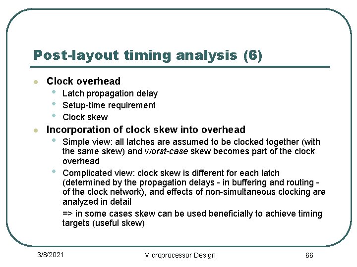
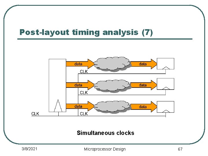
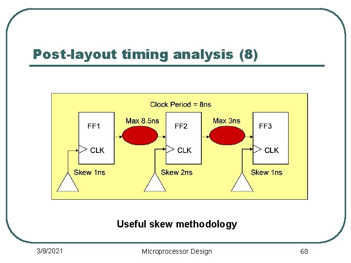
Post-layout timing analysis (6) l l Clock overhead • • • Latch propagation delay Setup-time requirement Clock skew Incorporation of clock skew into overhead • • Simple view: all latches are assumed to be clocked together (with the same skew) and worst-case skew becomes part of the clock overhead Complicated view: clock skew is different for each latch (determined by the propagation delays - in buffering and routing of the clock network), and effects of non-simultaneous clocking are analyzed in detail => in some cases skew can be used beneficially to achieve timing targets (useful skew) 3/8/2021 Microprocessor Design 66

Post-layout timing analysis (7) Simultaneous clocks 3/8/2021 Microprocessor Design 67

Post-layout timing analysis (8) Useful skew methodology 3/8/2021 Microprocessor Design 68

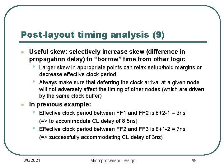
Post-layout timing analysis (9) l Useful skew: selectively increase skew (difference in propagation delay) to “borrow” time from other logic • • l Larger skew in appropriate points can relax setup/hold margins or decrease effective clock period Always make sure that deferring the clock arrival at a given node will not adversely affect the timing of other nodes (which are driven by the same clock buffer) In previous example: • • Effective clock period between FF 1 and FF 2 is 8+2 -1 = 9 ns (=> to accommodate CL delay of 8. 5 ns) Effective clock period between FF 2 and FF 3 is 8+1 -2 = 7 ns (=> successfully accommodating CL delay of 3 ns) 3/8/2021 Microprocessor Design 69

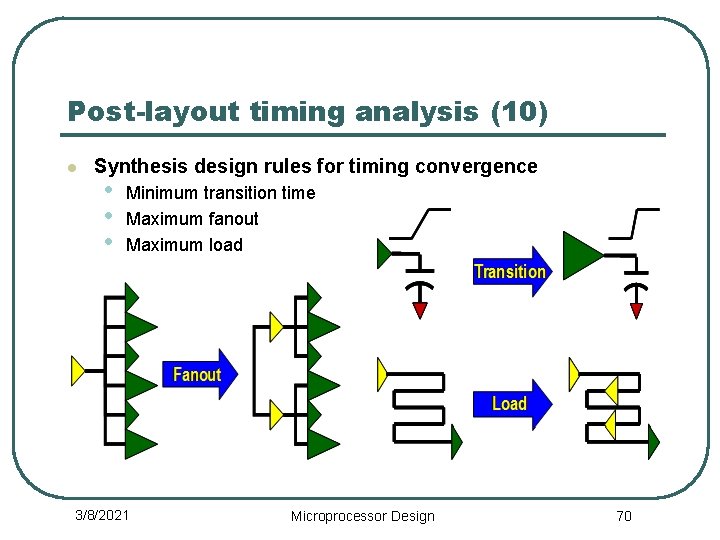
Post-layout timing analysis (10) l Synthesis design rules for timing convergence • • • Minimum transition time Maximum fanout Maximum load 3/8/2021 Microprocessor Design 70

Power analysis (1) 3/8/2021 Microprocessor Design 71

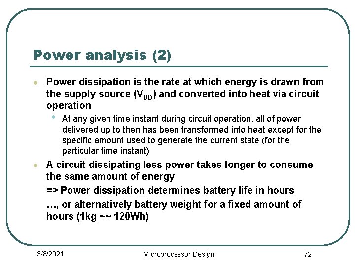
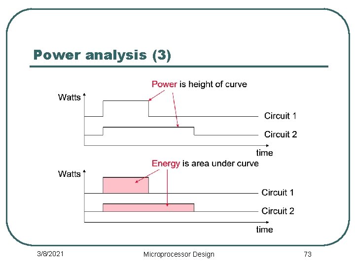
Power analysis (2) l Power dissipation is the rate at which energy is drawn from the supply source (VDD) and converted into heat via circuit operation • l At any given time instant during circuit operation, all of power delivered up to then has been transformed into heat except for the specific amount used to generate the current state (for the particular time instant) A circuit dissipating less power takes longer to consume the same amount of energy => Power dissipation determines battery life in hours …, or alternatively battery weight for a fixed amount of hours (1 kg ~~ 120 Wh) 3/8/2021 Microprocessor Design 72

Power analysis (3) 3/8/2021 Microprocessor Design 73

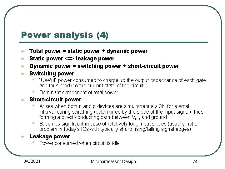
Power analysis (4) l l Total power = static power + dynamic power Static power <=> leakage power Dynamic power = switching power + short-circuit power Switching power • • l Short-circuit power • • l “Useful” power consumed to charge up the output capacitance of each gate and thus produce the current state of the circuit Dominant component of total power Arises when both n and p devices are simultaneously ON for a small interval during switching (determined by the slope of the input signal), thus forming a direct conducting path between VDD and ground Becomes significant in case of relatively long input slopes (usually not a problem in today’s ICs with typically sharp rising/falling signal edges) Leakage power • Power consumed when circuit is idle 3/8/2021 Microprocessor Design 74

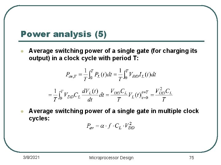
Power analysis (5) l Average switching power of a single gate (for charging its output) in a clock cycle with period T: l Average switching power of a single gate in multiple clock cycles: 3/8/2021 Microprocessor Design 75

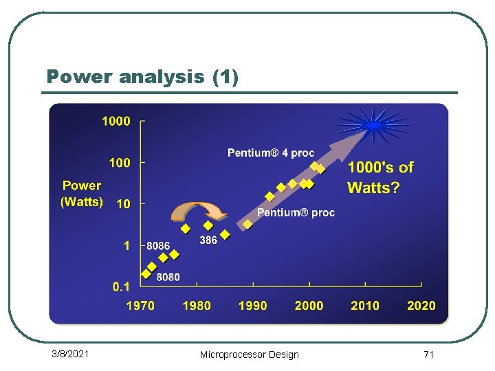
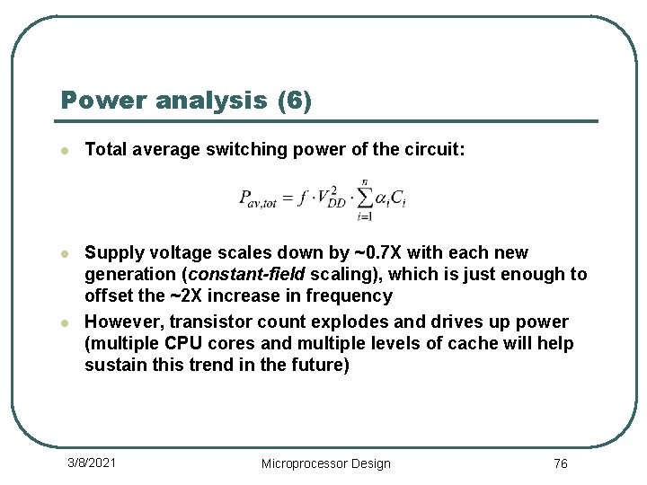
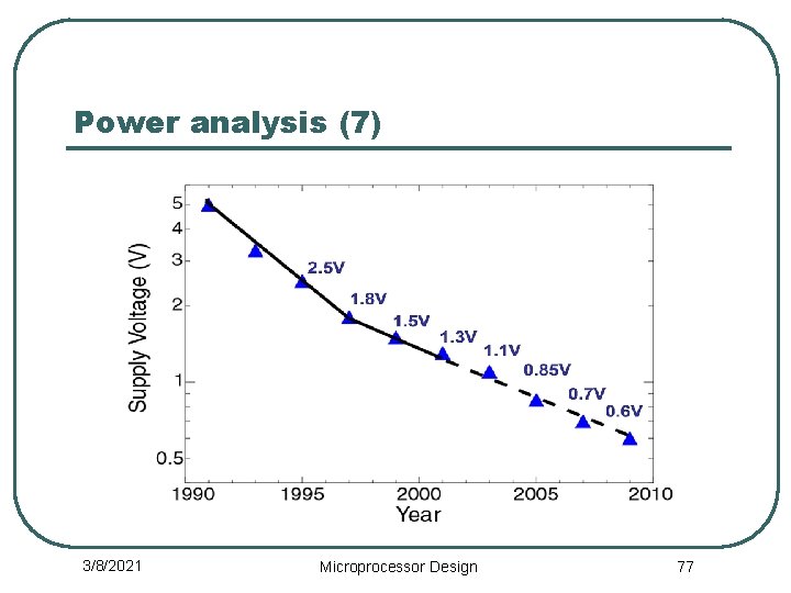
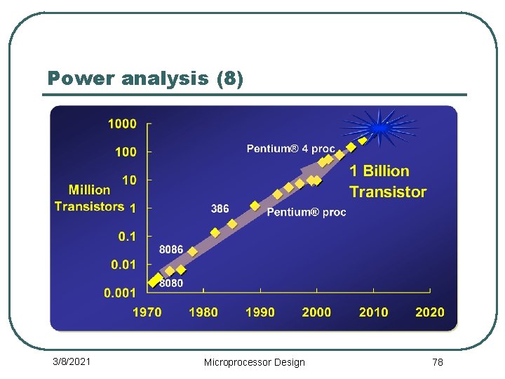
Power analysis (6) l Total average switching power of the circuit: l Supply voltage scales down by ~0. 7 X with each new generation (constant-field scaling), which is just enough to offset the ~2 X increase in frequency However, transistor count explodes and drives up power (multiple CPU cores and multiple levels of cache will help sustain this trend in the future) l 3/8/2021 Microprocessor Design 76

Power analysis (7) 3/8/2021 Microprocessor Design 77

Power analysis (8) 3/8/2021 Microprocessor Design 78

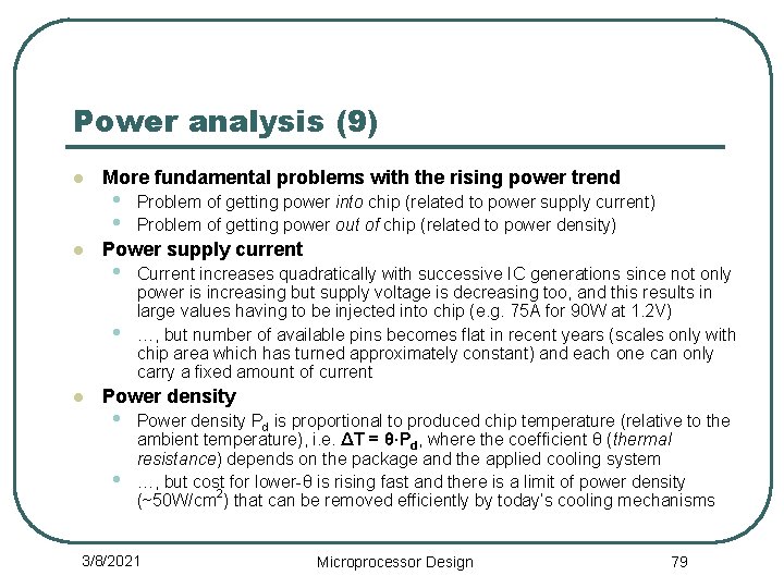
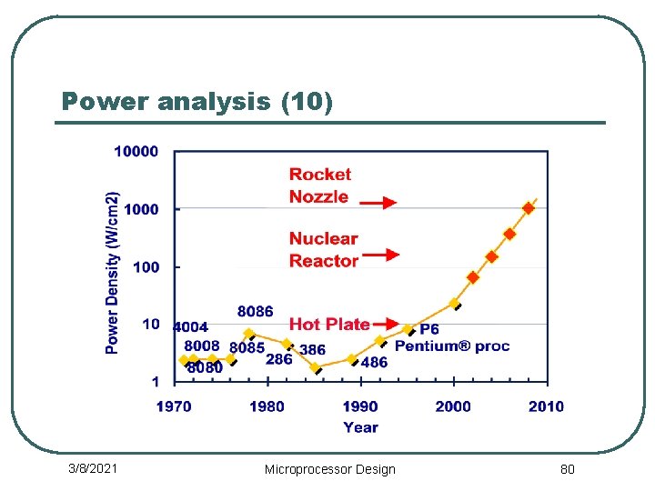
Power analysis (9) l l More fundamental problems with the rising power trend • • Power supply current • • l Problem of getting power into chip (related to power supply current) Problem of getting power out of chip (related to power density) Current increases quadratically with successive IC generations since not only power is increasing but supply voltage is decreasing too, and this results in large values having to be injected into chip (e. g. 75 A for 90 W at 1. 2 V) …, but number of available pins becomes flat in recent years (scales only with chip area which has turned approximately constant) and each one can only carry a fixed amount of current Power density • • Power density Pd is proportional to produced chip temperature (relative to the ambient temperature), i. e. ΔΤ = θ·Pd, where the coefficient θ (thermal resistance) depends on the package and the applied cooling system …, but cost for lower-θ is rising fast and there is a limit of power density (~50 W/cm 2) that can be removed efficiently by today’s cooling mechanisms 3/8/2021 Microprocessor Design 79

Power analysis (10) 3/8/2021 Microprocessor Design 80

Power analysis (11) l Types of power analysis • • Static (vectorless) power analysis Dynamic power analysis (for appropriate set of input vectors) [the above only refer to the analysis of dynamic switching power and are not to be confused with the static and dynamic components of total power] l Static power analysis • • l Each gate is assigned a static (i. e. vectorless) average power consumption and total power is computed as the sum of individual power values Problem: not very accurate since switching activity factor α depends on the sequence of input vectors being applied during operation Dynamic power analysis • • Simulation of the circuit under a representative set of input vectors Problem: operating vectors are not known in advance and it is impractical to perform simulation for a very large sequence 3/8/2021 Microprocessor Design 81

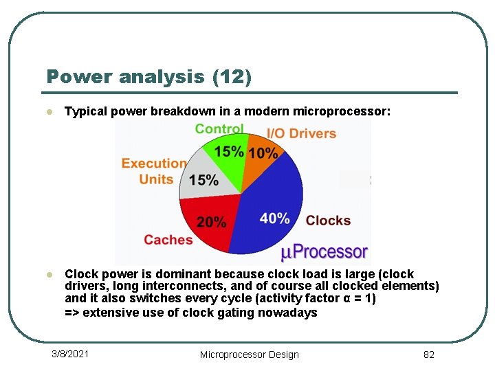
Power analysis (12) l Typical power breakdown in a modern microprocessor: l Clock power is dominant because clock load is large (clock drivers, long interconnects, and of course all clocked elements) and it also switches every cycle (activity factor α = 1) => extensive use of clock gating nowadays 3/8/2021 Microprocessor Design 82

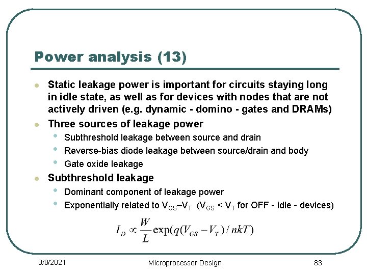
Power analysis (13) l l l Static leakage power is important for circuits staying long in idle state, as well as for devices with nodes that are not actively driven (e. g. dynamic - domino - gates and DRAMs) Three sources of leakage power • • • Subthreshold leakage between source and drain Reverse-bias diode leakage between source/drain and body Gate oxide leakage Subthreshold leakage • • Dominant component of leakage power Exponentially related to VGS–VT (VGS < VT for OFF - idle - devices) 3/8/2021 Microprocessor Design 83

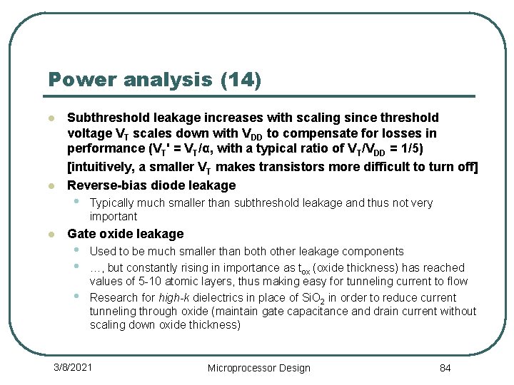
Power analysis (14) l l l Subthreshold leakage increases with scaling since threshold voltage VT scales down with VDD to compensate for losses in performance (VT' = VT/α, with a typical ratio of VT/VDD = 1/5) [intuitively, a smaller VT makes transistors more difficult to turn off] Reverse-bias diode leakage • Typically much smaller than subthreshold leakage and thus not very important Gate oxide leakage • • • Used to be much smaller than both other leakage components …, but constantly rising in importance as tox (oxide thickness) has reached values of 5 -10 atomic layers, thus making easy for tunneling current to flow Research for high-k dielectrics in place of Si. O 2 in order to reduce current tunneling through oxide (maintain gate capacitance and drain current without scaling down oxide thickness) 3/8/2021 Microprocessor Design 84

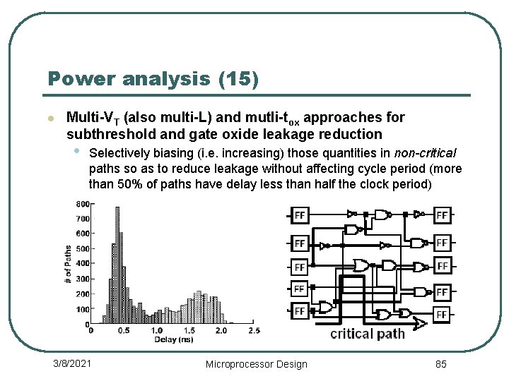
Power analysis (15) l Multi-VT (also multi-L) and mutli-tox approaches for subthreshold and gate oxide leakage reduction • Selectively biasing (i. e. increasing) those quantities in non-critical paths so as to reduce leakage without affecting cycle period (more than 50% of paths have delay less than half the clock period) 3/8/2021 Microprocessor Design 85

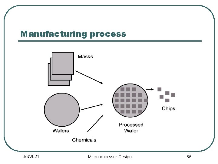
Manufacturing process 3/8/2021 Microprocessor Design 86

3/8/2021 Microprocessor Design 87