Chapter 9 Design of a Pipelined RISC Microprocessor
![• Pseudocode (RTL) solution: – 1. Fetch M[PC] into instruction register IR – • Pseudocode (RTL) solution: – 1. Fetch M[PC] into instruction register IR –](https://slidetodoc.com/presentation_image/81bce4a77cab401189cfe961a738f99d/image-8.jpg)
![• Example of fixed-length instruction formats used in the MIPS microprocessor [Lee 2000] • Example of fixed-length instruction formats used in the MIPS microprocessor [Lee 2000]](https://slidetodoc.com/presentation_image/81bce4a77cab401189cfe961a738f99d/image-10.jpg)
![• Variable-length instruction formats used in the Intel 8080 architecture [Lee 2000] 9/25/2020 • Variable-length instruction formats used in the Intel 8080 architecture [Lee 2000] 9/25/2020](https://slidetodoc.com/presentation_image/81bce4a77cab401189cfe961a738f99d/image-11.jpg)
![[Lee 2000] How many data operands do THUMB instructions use? 9/25/2020 "Advanced Digital Logic [Lee 2000] How many data operands do THUMB instructions use? 9/25/2020 "Advanced Digital Logic](https://slidetodoc.com/presentation_image/81bce4a77cab401189cfe961a738f99d/image-13.jpg)
![Hardwired Control Using EPROMs Other PLD types can also be used [Lee 2000] 9/25/2020 Hardwired Control Using EPROMs Other PLD types can also be used [Lee 2000] 9/25/2020](https://slidetodoc.com/presentation_image/81bce4a77cab401189cfe961a738f99d/image-48.jpg)
![[Lee 2000] 9/25/2020 "Advanced Digital Logic Design" by Sunggu Lee 51 [Lee 2000] 9/25/2020 "Advanced Digital Logic Design" by Sunggu Lee 51](https://slidetodoc.com/presentation_image/81bce4a77cab401189cfe961a738f99d/image-51.jpg)
![[Lee 2000] 9/25/2020 "Advanced Digital Logic Design" by Sunggu Lee 52 [Lee 2000] 9/25/2020 "Advanced Digital Logic Design" by Sunggu Lee 52](https://slidetodoc.com/presentation_image/81bce4a77cab401189cfe961a738f99d/image-52.jpg)
![9/25/2020 [Lee 2000] "Advanced Digital Logic Design" by Sunggu Lee 53 9/25/2020 [Lee 2000] "Advanced Digital Logic Design" by Sunggu Lee 53](https://slidetodoc.com/presentation_image/81bce4a77cab401189cfe961a738f99d/image-53.jpg)
![9/25/2020 "Advanced Digital Logic Design" by Sunggu Lee [Lee 2000] 54 9/25/2020 "Advanced Digital Logic Design" by Sunggu Lee [Lee 2000] 54](https://slidetodoc.com/presentation_image/81bce4a77cab401189cfe961a738f99d/image-54.jpg)
- Slides: 54

Chapter 9: Design of a Pipelined RISC Microprocessor • Main Concepts to be Learned – Basic operation of a microprocessor • How to design a basic microprocessor circuit – Design of an instruction pipeline for a RISC microprocessor – Instruction set and circuit implementation of a commercial microprocessor • Uses THUMB microprocessor as an example – Pipelined microprocessor design "Advanced Digital Logic Design" by Sunggu Lee

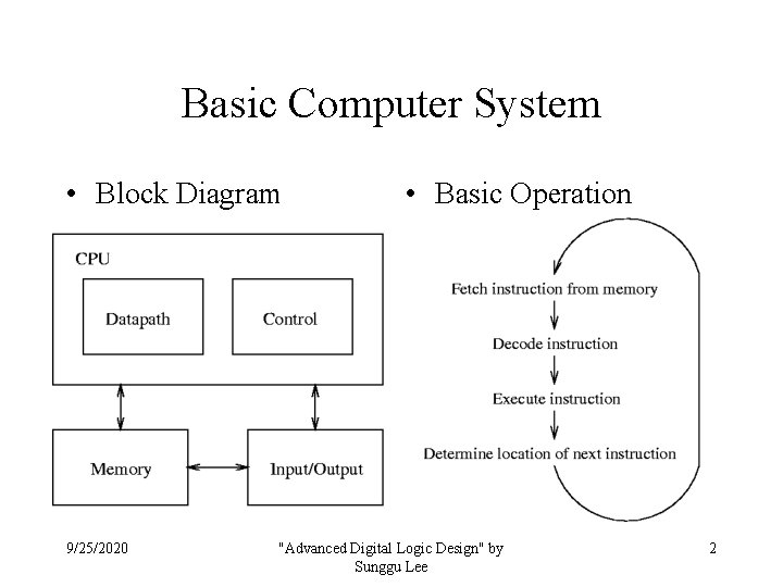
Basic Computer System • Block Diagram 9/25/2020 • Basic Operation "Advanced Digital Logic Design" by Sunggu Lee 2

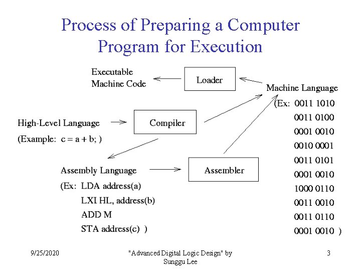
Process of Preparing a Computer Program for Execution 9/25/2020 "Advanced Digital Logic Design" by Sunggu Lee 3

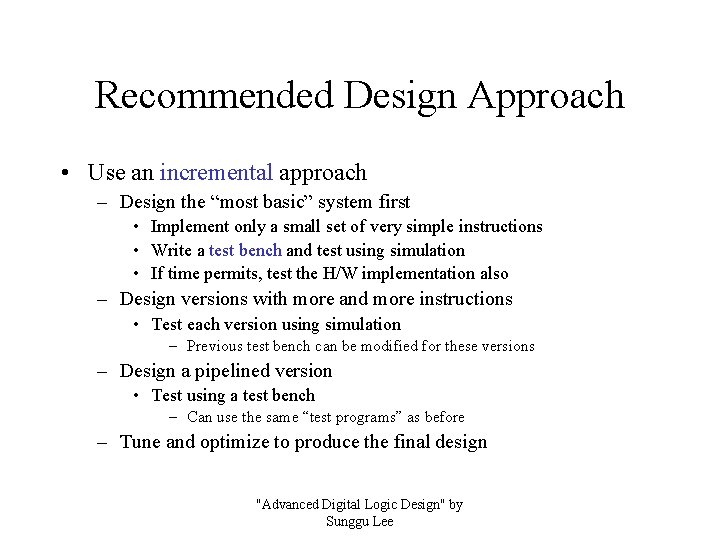
Recommended Design Approach • Use an incremental approach – Design the “most basic” system first • Implement only a small set of very simple instructions • Write a test bench and test using simulation • If time permits, test the H/W implementation also – Design versions with more and more instructions • Test each version using simulation – Previous test bench can be modified for these versions – Design a pipelined version • Test using a test bench – Can use the same “test programs” as before – Tune and optimize to produce the final design "Advanced Digital Logic Design" by Sunggu Lee

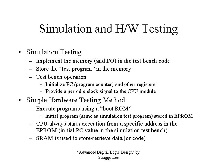
Simulation and H/W Testing • Simulation Testing – Implement the memory (and I/O) in the test bench code – Store the “test program” in the memory – Test bench operation • Initialize PC (program counter) and other registers • Provide a periodic clock signal to the CPU module • Simple Hardware Testing Method – Execute programs using a “boot ROM” • initial program (same as simulation test program) stored in EPROM – CPU always starts execution from a specific address in the EPROM (initial PC value in the simulation test bench) – SRAM is used to store/retrieve data (or code) "Advanced Digital Logic Design" by Sunggu Lee

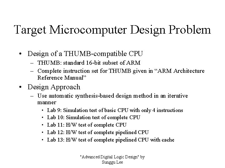
Target Microcomputer Design Problem • Design of a THUMB-compatible CPU – THUMB: standard 16 -bit subset of ARM – Complete instruction set for THUMB given in “ARM Architecture Reference Manual” • Design Approach – Use automatic synthesis-based design method in an iterative manner • • • Lab 9: Simulation test of basic CPU with only 4 instructions Lab 10: Simulation test of complete CPU Lab 11: H/W test of complete CPU Lab 12: H/W test of complete pipelined CPU Lab 13: H/W test of complete pipelined CPU with cache "Advanced Digital Logic Design" by Sunggu Lee

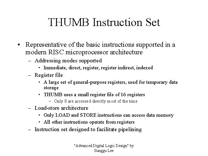
THUMB Instruction Set • Representative of the basic instructions supported in a modern RISC microprocessor architecture – Addressing modes supported • Immediate, direct, register indirect, indexed – Register file • A large set of general-purpose registers, used for temporary data storage • THUMB uses a small register file of 16 registers – Only 8 are accessed directly most of the time – Load-store architecture • Only LOAD and STORE instructions can access data memory • All other instructions operate from registers – Instruction set designed to facilitate pipelining "Advanced Digital Logic Design" by Sunggu Lee
![Pseudocode RTL solution 1 Fetch MPC into instruction register IR • Pseudocode (RTL) solution: – 1. Fetch M[PC] into instruction register IR –](https://slidetodoc.com/presentation_image/81bce4a77cab401189cfe961a738f99d/image-8.jpg)
• Pseudocode (RTL) solution: – 1. Fetch M[PC] into instruction register IR – 2. Increment PC by 2 – 3. Switch (IR) begin case “MOV Rd, Rn”: Rd Rn; case “ADD Rd, Rn, Rm”: Rd Rn + Rm; case “B #immed 3”: PC + immed 3; … end; – 4. Repeat from Step 1 9/25/2020 "Advanced Digital Logic Design" by Sunggu Lee 8

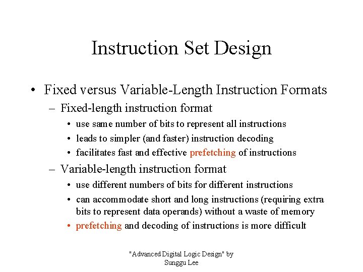
Instruction Set Design • Fixed versus Variable-Length Instruction Formats – Fixed-length instruction format • use same number of bits to represent all instructions • leads to simpler (and faster) instruction decoding • facilitates fast and effective prefetching of instructions – Variable-length instruction format • use different numbers of bits for different instructions • can accommodate short and long instructions (requiring extra bits to represent data operands) without a waste of memory • prefetching and decoding of instructions is more difficult "Advanced Digital Logic Design" by Sunggu Lee
![Example of fixedlength instruction formats used in the MIPS microprocessor Lee 2000 • Example of fixed-length instruction formats used in the MIPS microprocessor [Lee 2000]](https://slidetodoc.com/presentation_image/81bce4a77cab401189cfe961a738f99d/image-10.jpg)
• Example of fixed-length instruction formats used in the MIPS microprocessor [Lee 2000] 9/25/2020 "Advanced Digital Logic Design" by Sunggu Lee 10
![Variablelength instruction formats used in the Intel 8080 architecture Lee 2000 9252020 • Variable-length instruction formats used in the Intel 8080 architecture [Lee 2000] 9/25/2020](https://slidetodoc.com/presentation_image/81bce4a77cab401189cfe961a738f99d/image-11.jpg)
• Variable-length instruction formats used in the Intel 8080 architecture [Lee 2000] 9/25/2020 "Advanced Digital Logic Design" by Sunggu Lee 11

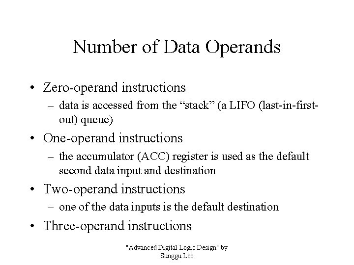
Number of Data Operands • Zero-operand instructions – data is accessed from the “stack” (a LIFO (last-in-firstout) queue) • One-operand instructions – the accumulator (ACC) register is used as the default second data input and destination • Two-operand instructions – one of the data inputs is the default destination • Three-operand instructions "Advanced Digital Logic Design" by Sunggu Lee
![Lee 2000 How many data operands do THUMB instructions use 9252020 Advanced Digital Logic [Lee 2000] How many data operands do THUMB instructions use? 9/25/2020 "Advanced Digital Logic](https://slidetodoc.com/presentation_image/81bce4a77cab401189cfe961a738f99d/image-13.jpg)
[Lee 2000] How many data operands do THUMB instructions use? 9/25/2020 "Advanced Digital Logic Design" by Sunggu Lee 13

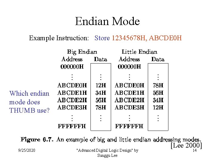
Endian Mode Example Instruction: Store 12345678 H, ABCDE 0 H Which endian mode does THUMB use? 9/25/2020 "Advanced Digital Logic Design" by Sunggu Lee [Lee 2000] 14

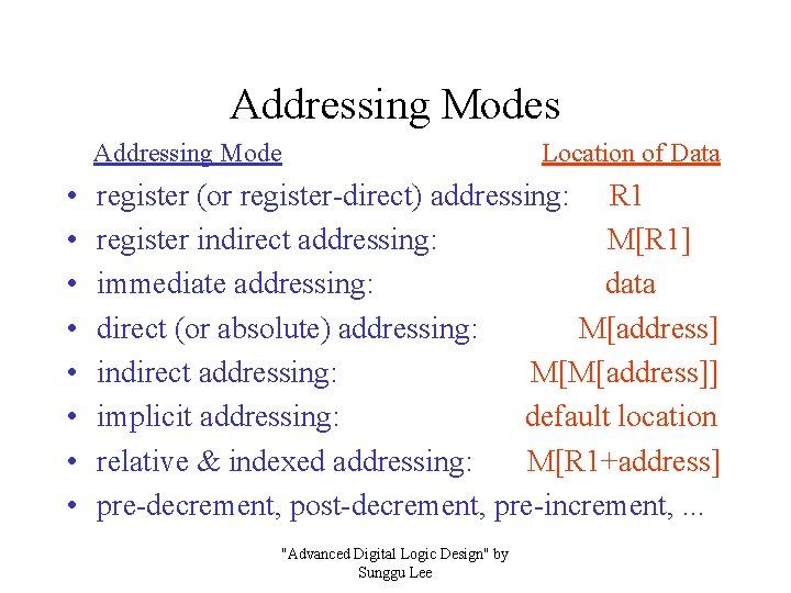
Addressing Modes Addressing Mode • • Location of Data register (or register-direct) addressing: R 1 register indirect addressing: M[R 1] immediate addressing: data direct (or absolute) addressing: M[address] indirect addressing: M[M[address]] implicit addressing: default location relative & indexed addressing: M[R 1+address] pre-decrement, post-decrement, pre-increment, . . . "Advanced Digital Logic Design" by Sunggu Lee

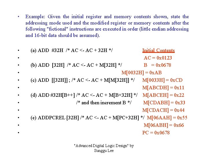
• Example: Given the initial register and memory contents shown, state the addressing mode used and the modified register or memory contents after the following "fictional" instructions are executed in order (little endian addressing and 16 -bit data should be assumed). • • • (a) ADD #32 H /* AC <- AC + 32 H */ Initial Contents AC = 0 x 0123 (b) ADD [32 H] /* AC <- AC + M[32 H] */ B = 0 x 0678 M[0032 H] = 0 x. AB (c) ADD [[32 H]] ; /* AC <- AC + M[M[32 H]] */ M[0033 H] = 0 x. CD M[ABCDH] = 0 x 11 (d) ADD #32 H[B++] /* AC <- AC + M[B+32 H] */ M[ABCEH] = 0 x 22 /* and then increment B */ M[CDABH] = 0 x 33 M[CDACH] = 0 x 44 (e) ADDPCREL [32 H] /* AC <- AC + M[PC+32 H] */ M[06 AAH] = 0 x 55 M[06 ABH] = 0 x 66 PC = 0 x 0678 "Advanced Digital Logic Design" by Sunggu Lee

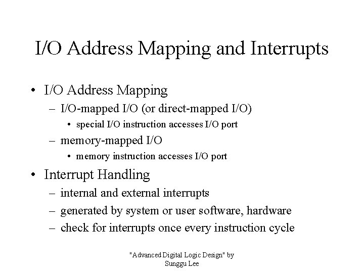
I/O Address Mapping and Interrupts • I/O Address Mapping – I/O-mapped I/O (or direct-mapped I/O) • special I/O instruction accesses I/O port – memory-mapped I/O • memory instruction accesses I/O port • Interrupt Handling – internal and external interrupts – generated by system or user software, hardware – check for interrupts once every instruction cycle "Advanced Digital Logic Design" by Sunggu Lee

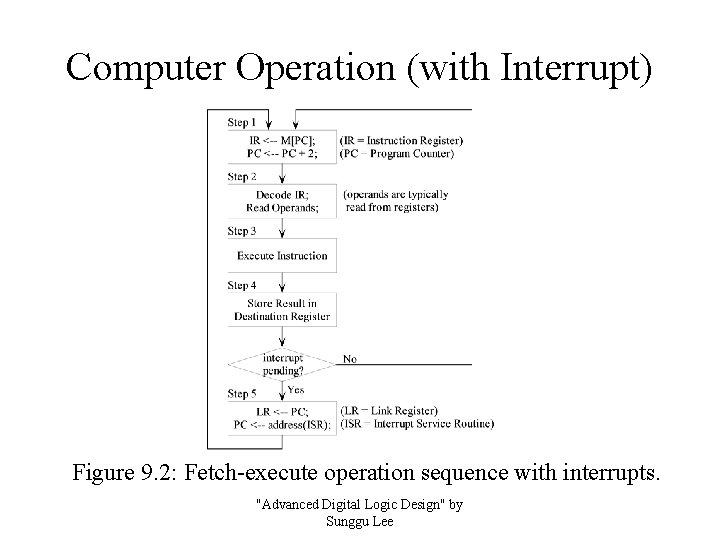
Computer Operation (with Interrupt) Figure 9. 2: Fetch-execute operation sequence with interrupts. "Advanced Digital Logic Design" by Sunggu Lee

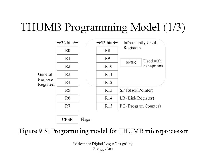
THUMB Programming Model (1/3) Figure 9. 3: Programming model for THUMB microprocessor "Advanced Digital Logic Design" by Sunggu Lee

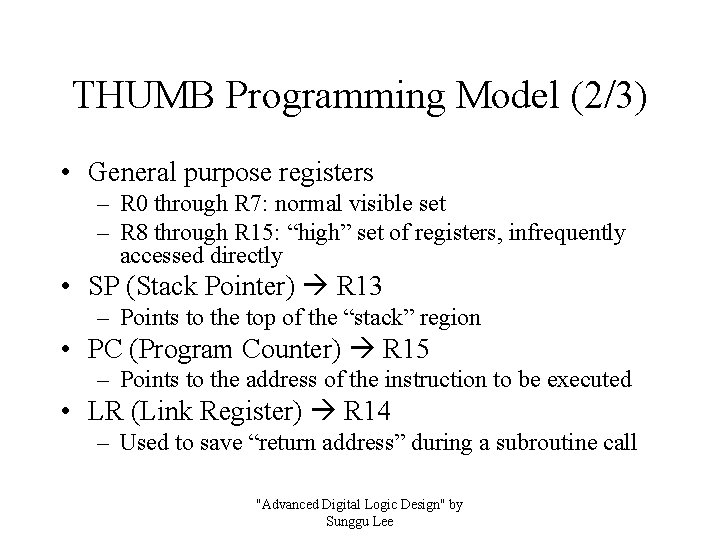
THUMB Programming Model (2/3) • General purpose registers – R 0 through R 7: normal visible set – R 8 through R 15: “high” set of registers, infrequently accessed directly • SP (Stack Pointer) R 13 – Points to the top of the “stack” region • PC (Program Counter) R 15 – Points to the address of the instruction to be executed • LR (Link Register) R 14 – Used to save “return address” during a subroutine call "Advanced Digital Logic Design" by Sunggu Lee

THUMB Programming Model (3/3) • Condition code bits (flags) – Stored in two “status” registers • CPSR (Current Program Status Register) – Contains most widely used flag bits • SPSR (Saved Program Status Register) – Used for interrupt (exception) processing • Commonly used condition code (flag) bits – negative (N), zero (Z), carry (C), overflow (O) "Advanced Digital Logic Design" by Sunggu Lee

THUMB Instruction Set (1/4) • Subset of ARM instruction set • Main instruction types – Branch – Data processing – Load/store – Exception-related "Advanced Digital Logic Design" by Sunggu Lee

THUMB Instruction Set (2/4) • Branch Instructions – Unconditional branch • Branches to new location “PC+offset” (offset is positive or negative) – PC-relative or relative addressing – Conditional branch • Checks a set of flag bits (refer to condition code table) • If (condition satisfied) then PC new branch address else PC next sequential address location – Subroutine CALL • Must save previous PC value before branching – Previous PC value can be saved on stack (PUSH) or in LR • Subroutine call in THUMB “branch with link” (save PC in LR) "Advanced Digital Logic Design" by Sunggu Lee

THUMB Instruction Set (3/4) • Data processing instructions – Data movement instructions • Read from memory or a register, store in register • Read from a register, store into register or memory – Arithmetic instructions • Add, subtract, negate, multiply, divide, compare, test • Condition codes set based on operation result – Logical instructions • OR, AND, exclusive-OR – Shift and rotate instruction • Logical shift and rotate shift in ‘ 0’ bits • Arithmetic shift preserve “sign” (copy msb bit during right-shift) "Advanced Digital Logic Design" by Sunggu Lee

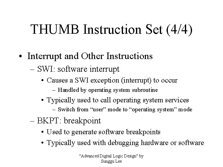
THUMB Instruction Set (4/4) • Interrupt and Other Instructions – SWI: software interrupt • Causes a SWI exception (interrupt) to occur – Handled by operating system subroutine • Typically used to call operating system services – Switch from “user” mode to “operating system” mode – BKPT: breakpoint • Used to generate software breakpoints • Typically used with debugging hardware or software "Advanced Digital Logic Design" by Sunggu Lee

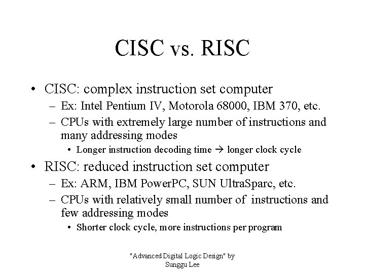
CISC vs. RISC • CISC: complex instruction set computer – Ex: Intel Pentium IV, Motorola 68000, IBM 370, etc. – CPUs with extremely large number of instructions and many addressing modes • Longer instruction decoding time longer clock cycle • RISC: reduced instruction set computer – Ex: ARM, IBM Power. PC, SUN Ultra. Sparc, etc. – CPUs with relatively small number of instructions and few addressing modes • Shorter clock cycle, more instructions per program "Advanced Digital Logic Design" by Sunggu Lee

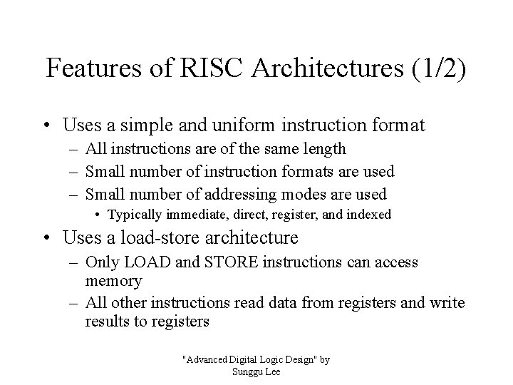
Features of RISC Architectures (1/2) • Uses a simple and uniform instruction format – All instructions are of the same length – Small number of instruction formats are used – Small number of addressing modes are used • Typically immediate, direct, register, and indexed • Uses a load-store architecture – Only LOAD and STORE instructions can access memory – All other instructions read data from registers and write results to registers "Advanced Digital Logic Design" by Sunggu Lee

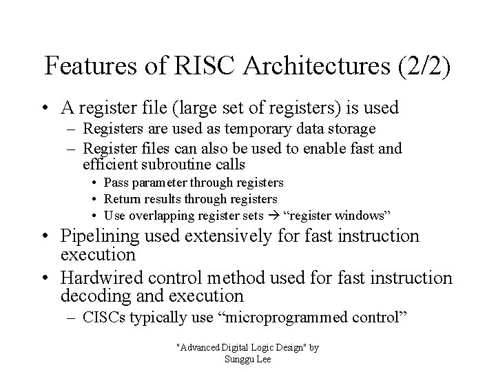
Features of RISC Architectures (2/2) • A register file (large set of registers) is used – Registers are used as temporary data storage – Register files can also be used to enable fast and efficient subroutine calls • Pass parameter through registers • Return results through registers • Use overlapping register sets “register windows” • Pipelining used extensively for fast instruction execution • Hardwired control method used for fast instruction decoding and execution – CISCs typically use “microprogrammed control” "Advanced Digital Logic Design" by Sunggu Lee

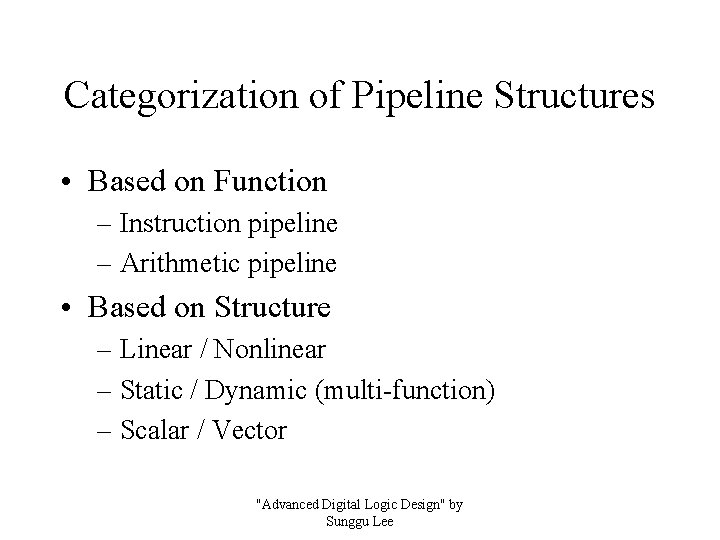
Categorization of Pipeline Structures • Based on Function – Instruction pipeline – Arithmetic pipeline • Based on Structure – Linear / Nonlinear – Static / Dynamic (multi-function) – Scalar / Vector "Advanced Digital Logic Design" by Sunggu Lee

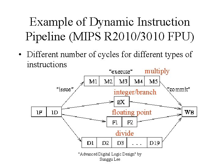
Example of Dynamic Instruction Pipeline (MIPS R 2010/3010 FPU) • Different number of cycles for different types of instructions multiply integer/branch floating point divide "Advanced Digital Logic Design" by Sunggu Lee

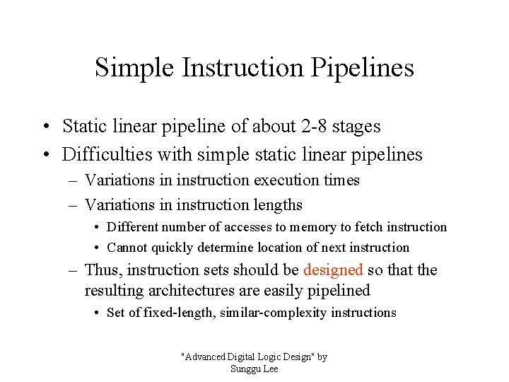
Simple Instruction Pipelines • Static linear pipeline of about 2 -8 stages • Difficulties with simple static linear pipelines – Variations in instruction execution times – Variations in instruction lengths • Different number of accesses to memory to fetch instruction • Cannot quickly determine location of next instruction – Thus, instruction sets should be designed so that the resulting architectures are easily pipelined • Set of fixed-length, similar-complexity instructions "Advanced Digital Logic Design" by Sunggu Lee

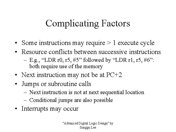
Complicating Factors • Some instructions may require > 1 execute cycle • Resource conflicts between successive instructions – E. g. , “LDR r 0, r 5, #5” followed by “LDR r 1, r 5, #6”: both require use of the memory • Next instruction may not be at PC+2 • Jumps or subroutine calls – Next instruction is not at next sequential location – Conditional jumps are also possible • Interrupts may occur "Advanced Digital Logic Design" by Sunggu Lee

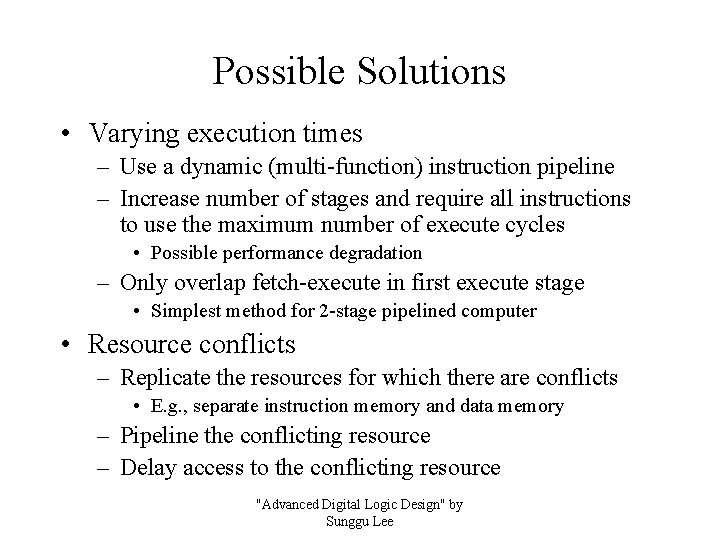
Possible Solutions • Varying execution times – Use a dynamic (multi-function) instruction pipeline – Increase number of stages and require all instructions to use the maximum number of execute cycles • Possible performance degradation – Only overlap fetch-execute in first execute stage • Simplest method for 2 -stage pipelined computer • Resource conflicts – Replicate the resources for which there are conflicts • E. g. , separate instruction memory and data memory – Pipeline the conflicting resource – Delay access to the conflicting resource "Advanced Digital Logic Design" by Sunggu Lee

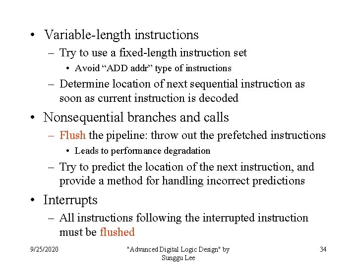
• Variable-length instructions – Try to use a fixed-length instruction set • Avoid “ADD addr” type of instructions – Determine location of next sequential instruction as soon as current instruction is decoded • Nonsequential branches and calls – Flush the pipeline: throw out the prefetched instructions • Leads to performance degradation – Try to predict the location of the next instruction, and provide a method for handling incorrect predictions • Interrupts – All instructions following the interrupted instruction must be flushed 9/25/2020 "Advanced Digital Logic Design" by Sunggu Lee 34

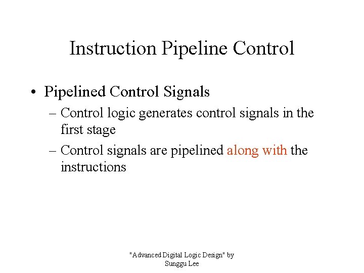
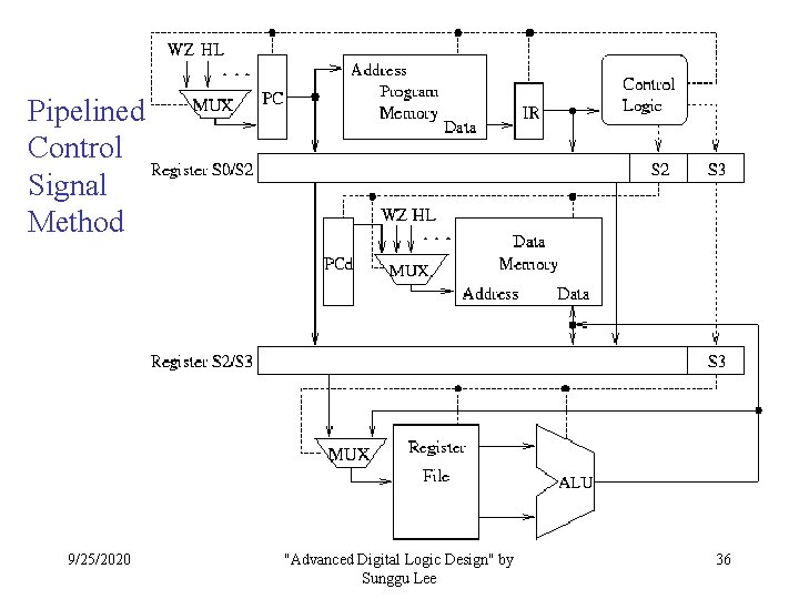
Instruction Pipeline Control • Pipelined Control Signals – Control logic generates control signals in the first stage – Control signals are pipelined along with the instructions "Advanced Digital Logic Design" by Sunggu Lee

Pipelined Control Signal Method 9/25/2020 "Advanced Digital Logic Design" by Sunggu Lee 36

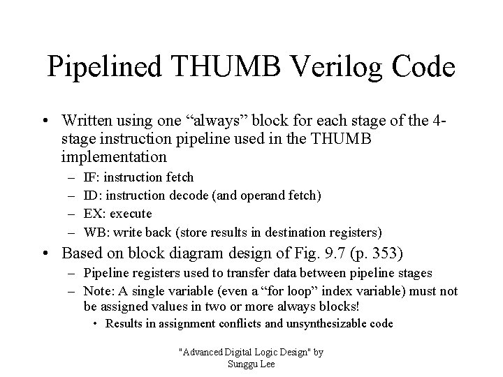
Pipelined THUMB Verilog Code • Written using one “always” block for each stage of the 4 stage instruction pipeline used in the THUMB implementation – – IF: instruction fetch ID: instruction decode (and operand fetch) EX: execute WB: write back (store results in destination registers) • Based on block diagram design of Fig. 9. 7 (p. 353) – Pipeline registers used to transfer data between pipeline stages – Note: A single variable (even a “for loop” index variable) must not be assigned values in two or more always blocks! • Results in assignment conflicts and unsynthesizable code "Advanced Digital Logic Design" by Sunggu Lee

Pipelined THUMB Block Diagram "Advanced Digital Logic Design" by Sunggu Lee

Pipeline Control (to be covered if time permits) • Controlling Initiation of “Pipeline Instructions” – Static linear pipelines • Start next instruction whenever conflicts can be avoided – Dynamic (multifunction) pipelines • More difficult to determine “optimal” instruction initiation time • Solution used for static linear pipelines is not the best "Advanced Digital Logic Design" by Sunggu Lee

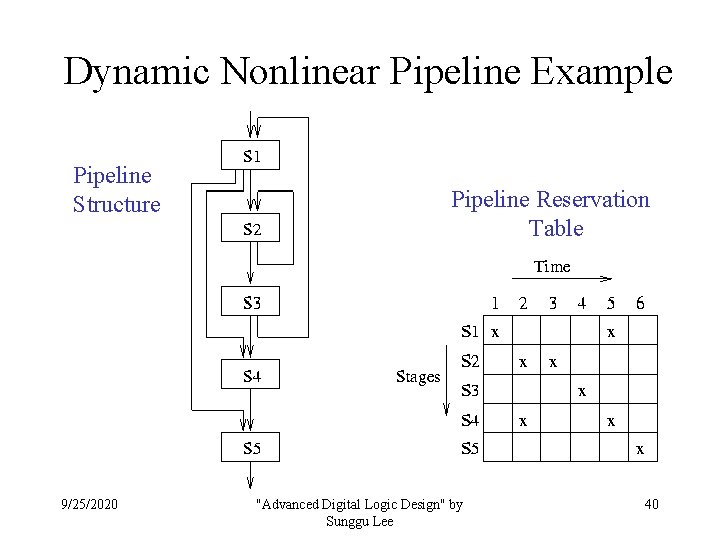
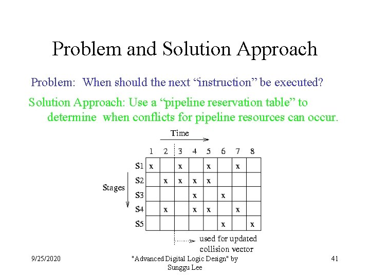
Dynamic Nonlinear Pipeline Example Pipeline Structure 9/25/2020 Pipeline Reservation Table "Advanced Digital Logic Design" by Sunggu Lee 40

Problem and Solution Approach Problem: When should the next “instruction” be executed? Solution Approach: Use a “pipeline reservation table” to determine when conflicts for pipeline resources can occur. 9/25/2020 "Advanced Digital Logic Design" by Sunggu Lee 41

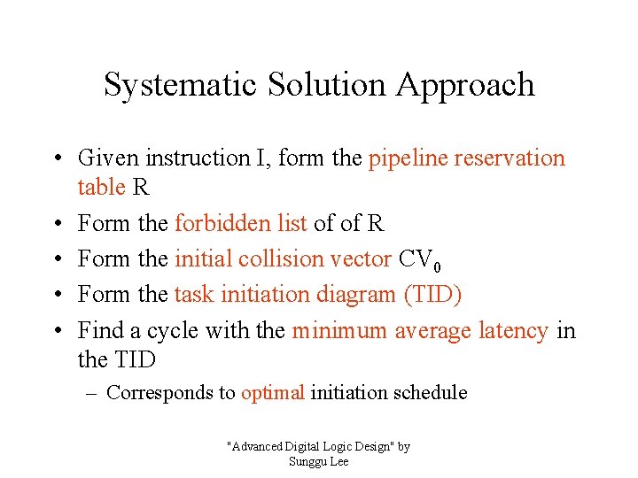
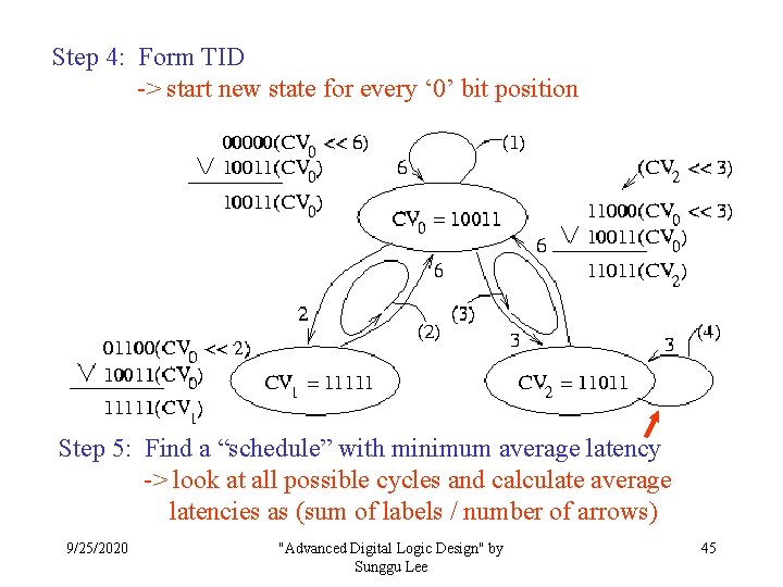
Systematic Solution Approach • Given instruction I, form the pipeline reservation table R • Form the forbidden list of of R • Form the initial collision vector CV 0 • Form the task initiation diagram (TID) • Find a cycle with the minimum average latency in the TID – Corresponds to optimal initiation schedule "Advanced Digital Logic Design" by Sunggu Lee

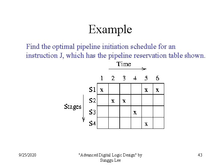
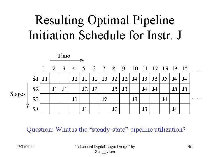
Example Find the optimal pipeline initiation schedule for an instruction J, which has the pipeline reservation table shown. 9/25/2020 "Advanced Digital Logic Design" by Sunggu Lee 43

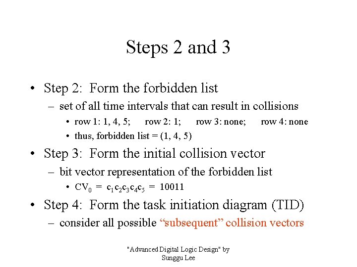
Steps 2 and 3 • Step 2: Form the forbidden list – set of all time intervals that can result in collisions • row 1: 1, 4, 5; row 2: 1; row 3: none; row 4: none • thus, forbidden list = (1, 4, 5) • Step 3: Form the initial collision vector – bit vector representation of the forbidden list • CV 0 = c 1 c 2 c 3 c 4 c 5 = 10011 • Step 4: Form the task initiation diagram (TID) – consider all possible “subsequent” collision vectors "Advanced Digital Logic Design" by Sunggu Lee

Step 4: Form TID -> start new state for every ‘ 0’ bit position Step 5: Find a “schedule” with minimum average latency -> look at all possible cycles and calculate average latencies as (sum of labels / number of arrows) 9/25/2020 "Advanced Digital Logic Design" by Sunggu Lee 45

Resulting Optimal Pipeline Initiation Schedule for Instr. J Question: What is the “steady-state” pipeline utilization? 9/25/2020 "Advanced Digital Logic Design" by Sunggu Lee 46

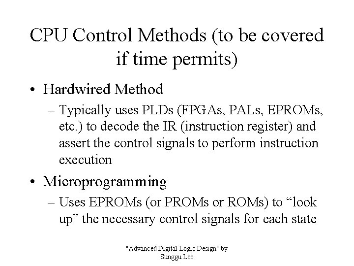
CPU Control Methods (to be covered if time permits) • Hardwired Method – Typically uses PLDs (FPGAs, PALs, EPROMs, etc. ) to decode the IR (instruction register) and assert the control signals to perform instruction execution • Microprogramming – Uses EPROMs (or PROMs or ROMs) to “look up” the necessary control signals for each state "Advanced Digital Logic Design" by Sunggu Lee
![Hardwired Control Using EPROMs Other PLD types can also be used Lee 2000 9252020 Hardwired Control Using EPROMs Other PLD types can also be used [Lee 2000] 9/25/2020](https://slidetodoc.com/presentation_image/81bce4a77cab401189cfe961a738f99d/image-48.jpg)
Hardwired Control Using EPROMs Other PLD types can also be used [Lee 2000] 9/25/2020 "Advanced Digital Logic Design" by Sunggu Lee 48

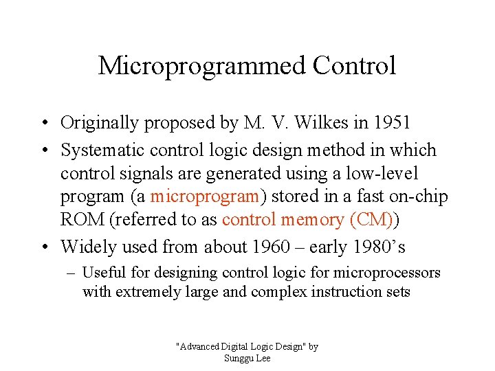
Microprogrammed Control • Originally proposed by M. V. Wilkes in 1951 • Systematic control logic design method in which control signals are generated using a low-level program (a microprogram) stored in a fast on-chip ROM (referred to as control memory (CM)) • Widely used from about 1960 – early 1980’s – Useful for designing control logic for microprocessors with extremely large and complex instruction sets "Advanced Digital Logic Design" by Sunggu Lee

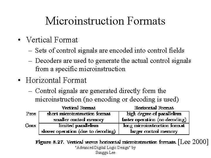
Microinstruction Formats • Vertical Format – Sets of control signals are encoded into control fields – Decoders are used to generate the actual control signals from a specific microinstruction • Horizontal Format – Control signals are generated directly form the microinstruction (no encoding or decoding is used) "Advanced Digital Logic Design" by Sunggu Lee [Lee 2000]
![Lee 2000 9252020 Advanced Digital Logic Design by Sunggu Lee 51 [Lee 2000] 9/25/2020 "Advanced Digital Logic Design" by Sunggu Lee 51](https://slidetodoc.com/presentation_image/81bce4a77cab401189cfe961a738f99d/image-51.jpg)
[Lee 2000] 9/25/2020 "Advanced Digital Logic Design" by Sunggu Lee 51
![Lee 2000 9252020 Advanced Digital Logic Design by Sunggu Lee 52 [Lee 2000] 9/25/2020 "Advanced Digital Logic Design" by Sunggu Lee 52](https://slidetodoc.com/presentation_image/81bce4a77cab401189cfe961a738f99d/image-52.jpg)
[Lee 2000] 9/25/2020 "Advanced Digital Logic Design" by Sunggu Lee 52
![9252020 Lee 2000 Advanced Digital Logic Design by Sunggu Lee 53 9/25/2020 [Lee 2000] "Advanced Digital Logic Design" by Sunggu Lee 53](https://slidetodoc.com/presentation_image/81bce4a77cab401189cfe961a738f99d/image-53.jpg)
9/25/2020 [Lee 2000] "Advanced Digital Logic Design" by Sunggu Lee 53
![9252020 Advanced Digital Logic Design by Sunggu Lee Lee 2000 54 9/25/2020 "Advanced Digital Logic Design" by Sunggu Lee [Lee 2000] 54](https://slidetodoc.com/presentation_image/81bce4a77cab401189cfe961a738f99d/image-54.jpg)
9/25/2020 "Advanced Digital Logic Design" by Sunggu Lee [Lee 2000] 54