MICROPROCESSOR THEORY AND INTERFACING Week8 INTERFACING Memory Organization

- Slides: 29

MICROPROCESSOR THEORY AND INTERFACING Week-8 INTERFACING

Memory Organization of 8086 • 8086 has a 20 bit address bus and hence it can address 2^20 or 1, 048, 576 addresses • Each location one byte is stored • Two consecutive memory locations are required for a word to store • Both memory read and memory write operations require more than one machine cycle • Memory organization is required to complete memory read and memory write operations to be completed with one machine cycle

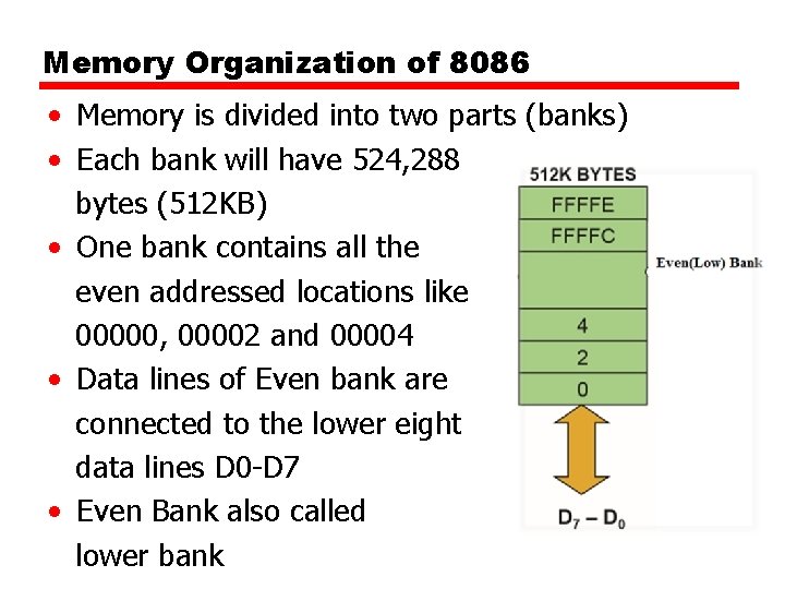
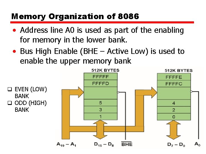
Memory Organization of 8086 • Memory is divided into two parts (banks) • Each bank will have 524, 288 bytes (512 KB) • One bank contains all the even addressed locations like 00000, 00002 and 00004 • Data lines of Even bank are connected to the lower eight data lines D 0 -D 7 • Even Bank also called lower bank

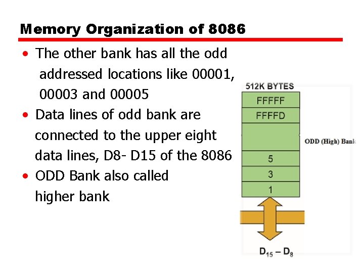
Memory Organization of 8086 • The other bank has all the odd addressed locations like 00001, 00003 and 00005 • Data lines of odd bank are connected to the upper eight data lines, D 8 - D 15 of the 8086 • ODD Bank also called higher bank

Memory Organization of 8086 • Address line A 0 is used as part of the enabling for memory in the lower bank. • Bus High Enable (BHE – Active Low) is used to enable the upper memory bank q EVEN (LOW) BANK q ODD (HIGH) BANK

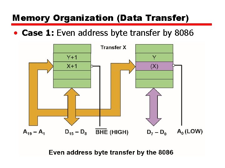
Memory Organization (Data Transfer) • • • Case 1: Even address byte transfer by 8086 Read/Write a byte form/to an even address A 0 will be low BHE (Active Low) will be high Byte is transferred to/from low bank through D 0 -D 7 • One Machine Cycle required • Example MOV AH, DS: BYTE PTR[0000]

Memory Organization (Data Transfer) • Case 1: Even address byte transfer by 8086

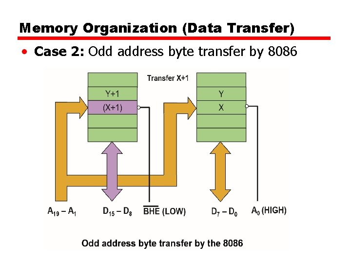
Memory Organization (Data Transfer) • • Case 2: Odd address byte transfer by 8086 Read/Write a byte from/to an odd address A 0 will be high BHE (Active Low) will be asserted low Low bank is disabled and high bank is enabled Byte is transferred through D 0 -D 7 One Machine Cycle required Example MOV AL, DS: BYTE PTR[0001]

Memory Organization (Data Transfer) • Case 2: Odd address byte transfer by 8086

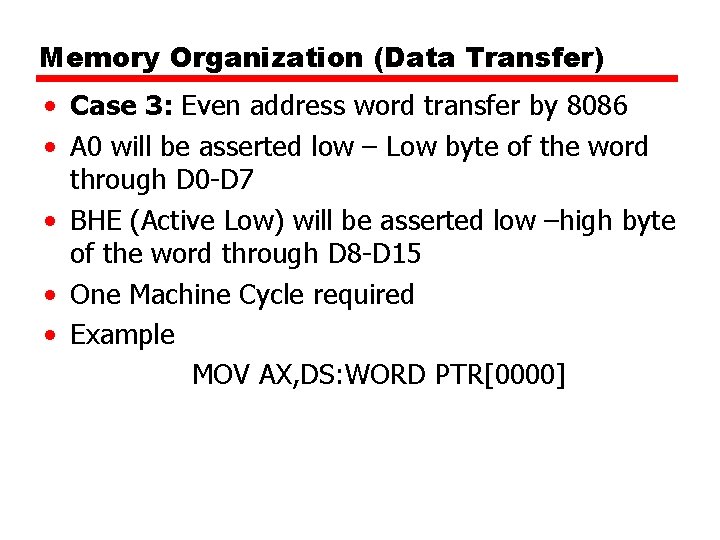
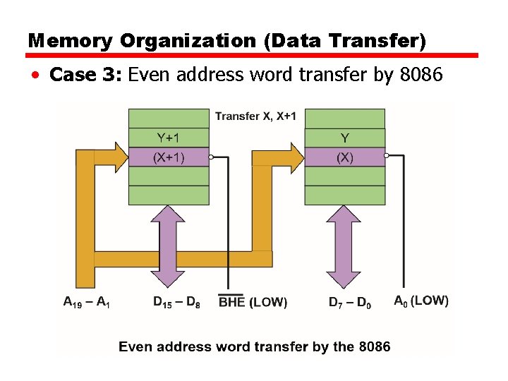
Memory Organization (Data Transfer) • Case 3: Even address word transfer by 8086 • A 0 will be asserted low – Low byte of the word through D 0 -D 7 • BHE (Active Low) will be asserted low –high byte of the word through D 8 -D 15 • One Machine Cycle required • Example MOV AX, DS: WORD PTR[0000]

Memory Organization (Data Transfer) • Case 3: Even address word transfer by 8086

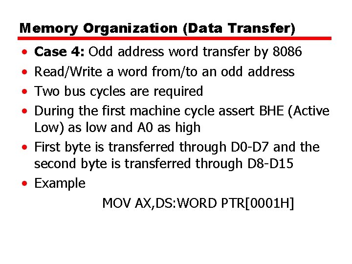
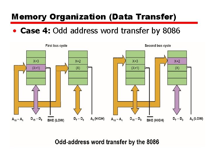
Memory Organization (Data Transfer) • • Case 4: Odd address word transfer by 8086 Read/Write a word from/to an odd address Two bus cycles are required During the first machine cycle assert BHE (Active Low) as low and A 0 as high • First byte is transferred through D 0 -D 7 and the second byte is transferred through D 8 -D 15 • Example MOV AX, DS: WORD PTR[0001 H]

Memory Organization (Data Transfer) • Case 4: Odd address word transfer by 8086

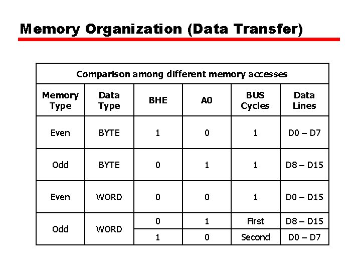
Memory Organization (Data Transfer) Comparison among different memory accesses Memory Type Data Type BHE A 0 BUS Cycles Data Lines Even BYTE 1 0 1 D 0 – D 7 Odd BYTE 0 1 1 D 8 – D 15 Even WORD 0 0 1 D 0 – D 15 0 1 First D 8 – D 15 1 0 Second D 0 – D 7 Odd WORD

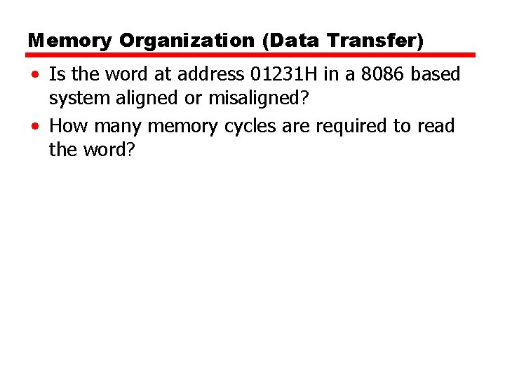
Memory Organization (Data Transfer) • Is the word at address 01231 H in a 8086 based system aligned or misaligned? • How many memory cycles are required to read the word?

Address Decoding Techniques • The Different types of address decoding techniques in 8086 Microprocessor are, 1. Absolute decoding 2. Linear decoding 3. Block decoding

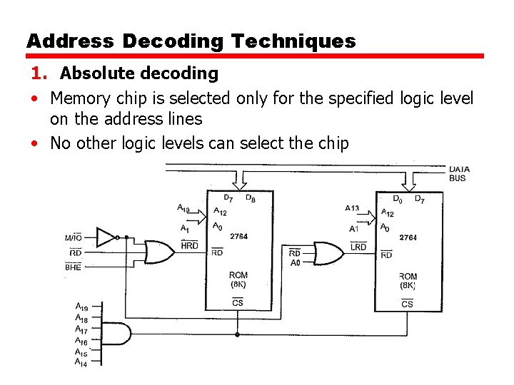
Address Decoding Techniques 1. Absolute decoding • Memory chip is selected only for the specified logic level on the address lines • No other logic levels can select the chip

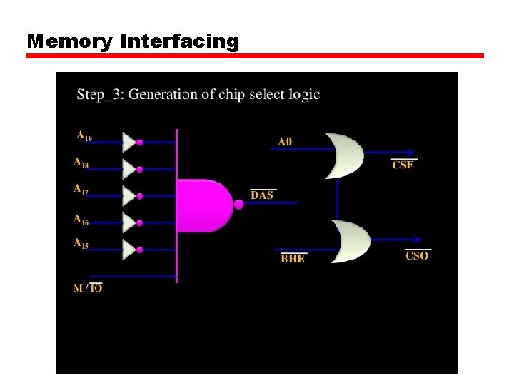
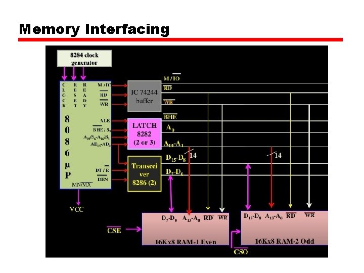
Address Decoding Techniques 1. Absolute decoding • Figure shows the memory interface with absolute decoding • Two 8 K EPROMs (2764) are used to provide even and odd memory banks • Control signals BHE and A 0 are used to enable outputs of odd and even memory banks respectively

Address Decoding Techniques 1. Absolute decoding • Each memory chip has 8 K memory locations, thirteen address lines are required to address each locations, independently • Remaining address lines are used to generate an unique chip select signal • This addressing technique is normally used in large, memory systems.

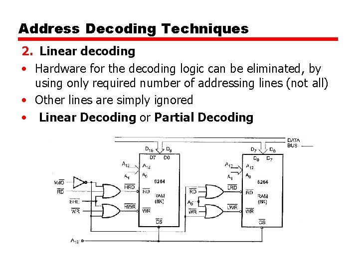
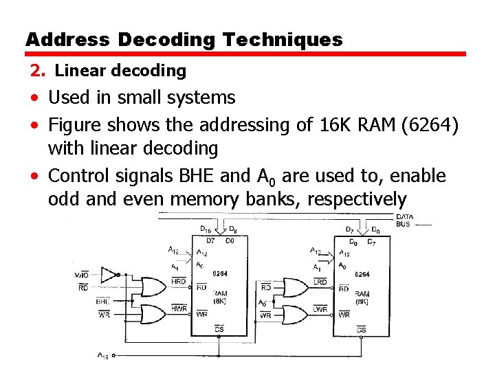
Address Decoding Techniques 2. Linear decoding • Hardware for the decoding logic can be eliminated, by using only required number of addressing lines (not all) • Other lines are simply ignored • Linear Decoding or Partial Decoding

Address Decoding Techniques 2. Linear decoding • Used in small systems • Figure shows the addressing of 16 K RAM (6264) with linear decoding • Control signals BHE and A 0 are used to, enable odd and even memory banks, respectively

Address Decoding Techniques 2. Linear decoding • RAM chips when A 19 is low, chip is selected • The status of A 14 to A 18 does not affect the chip selection logic • This gives you multiple addresses (shadow addresses) • This technique reduces the cost of Address Decoding Techniques in 8086 Microprocessor circuit, but it has drawback of multiple addresses

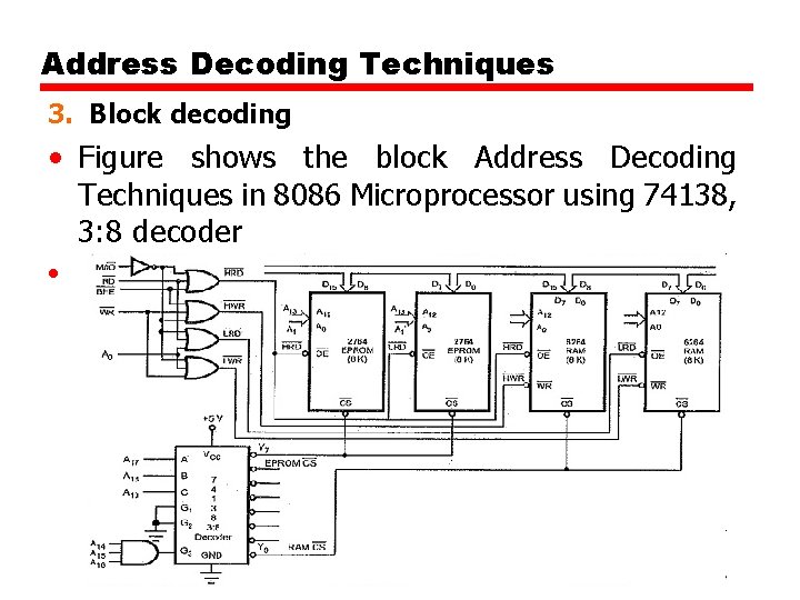
Address Decoding Techniques 3. Block decoding • In a microcomputer system the memory array is often consists of several blocks of memory chips • Each block of memory requires decoding circuit • To avoid separate decoding for each memory block special decoder IC is used to generate chip select signal for each block

Address Decoding Techniques 3. Block decoding • Figure shows the block Address Decoding Techniques in 8086 Microprocessor using 74138, 3: 8 decoder •

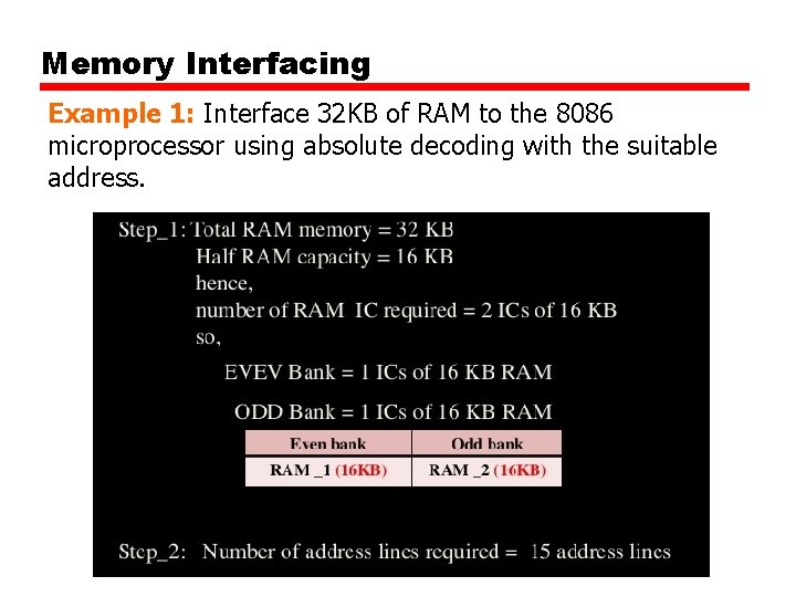
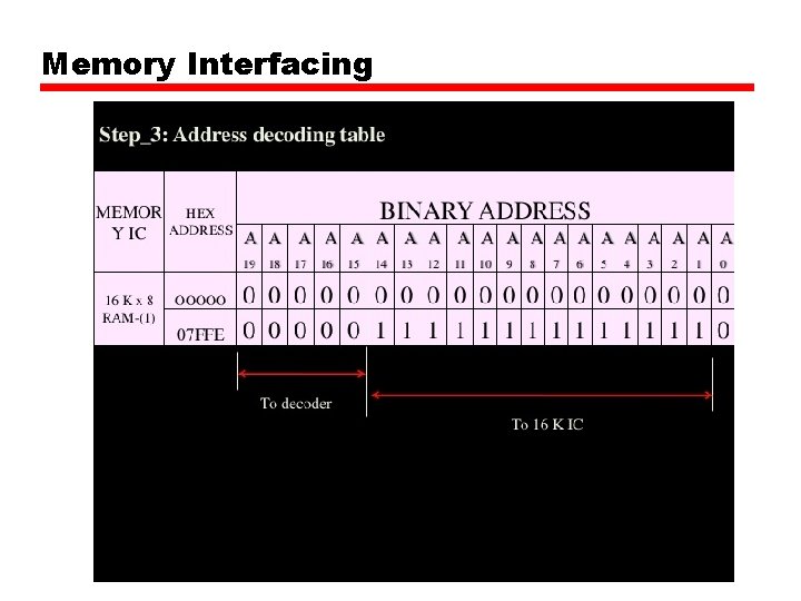
Memory Interfacing Example 1: Interface 32 KB of RAM to the 8086 microprocessor using absolute decoding with the suitable address.

Memory Interfacing

Memory Interfacing

Memory Interfacing

REVIEW