MICROPROCESSOR Accumulator The accumulator functions both as a

MICROPROCESSOR

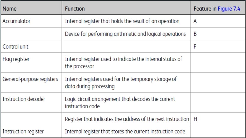
Accumulator : § The accumulator functions both as a source and as a destination register for many of the basic microprocessor operations. § As a source register it contains the data that will be used in a particular operation, while as a destination register it will be used to hold the result of a particular operation. § The accumulator (or A register) features in a very large number of microprocessor operations, consequently more reference is made to this register than any other.

Instruction register : § The instruction register provides a temporary storage location in which the current microprocessor instruction is held while it is being decoded. § Program instructions are passed into the microprocessor, one at a time, through the data bus. § On the first part of each machine cycle, the instruction is fetched and decoded. The instruction is executed on the second (and subsequent) machine cycles. § Each machine cycle takes a finite time (usually less than a microsecond) depending upon the frequency of the microprocessor’s clock.
 : The external data bus provides a")
Data bus (D 0 to D 7) : The external data bus provides a highway for data that links all of the system components (such as RAM, ROM and I/O devices) together. In an 8 -bit system, the data bus has eight data lines, labelled D 0 (the least significant bit) to D 7 (the most significant bit) and data are moved around in groups of eight bits, or bytes. With a 16 -bit data bus the data lines are labelled D 0 to D 15, and so on. Internal data bus : The internal data bus is a high-speed data highway that links all of the microprocessor’s internal elements together. Data is constantly flowing backwards and forwards along the internal data bus lines.

Data bus buffer : § The data bus buffer is a temporary register through which bytes of data pass on their way into and out of the microprocessor. § The buffer is thus referred to as bidirectional, with data passing out of the microprocessor on a write operation and into the processor during a read operation. § The direction of data transfer is determined by the control unit as it responds to each individual program instruction.

General purpose registers : § Many microprocessor operations (for example, adding two 8 -bit numbers together) require the use of more than one register. § There is also a requirement for temporarily storing the partial result of an operation while other operations take place. § Both of these needs can be met by providing a number of general purpose registers. The use to which these registers are put is left mainly up to the programmer.

Instruction pointer : § Computer programs consist of a sequence of instructions that are executed by the microprocessor. § These instructions are stored in external RAM or ROM. Instructions must be fetched and executed by the microprocessor in a strict sequence. § By storing the address of the next instruction to be executed, the instruction pointer (or program counter) allows the microprocessor to keep track of where it is within the program. § The program counter is automatically incremented when each instruction is executed

Stack pointer : § When the time comes to suspend a particular task in order to briefly attend to something else, most microprocessors make use of a region of external random access memory (RAM) known as a stack. § When the main program is interrupted, the microprocessor temporarily places in the stack the contents of its internal registers together with the address of the next instruction in the main program. § When the interrupt has been attended to, the microprocessor recovers the data that has been stored temporarily in the stack, together with the address of the next instruction within the main program. § It is thus able to return to the main program exactly where it left off and with all the data preserved in its registers. The stack pointer is simply a register containing the address of the last used stack location.

Address buffer : § The address buffer is a temporary register through which addresses (in this case comprising 16 -bits) pass on their way out of the microprocessor. § In a simple microprocessor, the address buffer is unidirectional with addresses placed on the address bus during both read and write operations. § The address bus lines are labelled A 0 to A 15, where A 0 is the least significant address bus line and A 15 is the most significant address bus line. § Note that a 16 -bit address bus can be used to communicate with 65, 536 individual memory locations. At each location a single byte of data is stored.

Control bus : The control bus is a collection of signal lines that are both used to control the transfer of data around the system and also to interact with external devices. The control signals used by microprocessors tend to differ with different types; however, the following are commonly found: INSTRUCTION FUNCTION READ An output signal from the CPU that indicates that the current operation is a read operation WRITE An output signal from the CPU that indicates that the current operation is a write operation. RESET A signal that resets the internal registers and initializes the instruction pointer program counter so that the program can be restarted from the beginning. IRQ An interrupt request from an external device attempting to gain the attention of the CPU (the request may either be obeyed or ignored according to the state of the microprocessor at the time that the interrupt request is received). NMI Non maskable interrupt (i. e. an interrupt signal that cannot be ignored by the microprocessor).
 : The address bus provides a highway")
Address bus (A 0 to A 15) : The address bus provides a highway for addresses that links with all of the system components (such as RAM, ROM and I/O devices). In a system with a 16 - bit address bus, there are 16 address lines, labelled A 0 (the least significant bit) to A 15 (the most significant bit). In a system with a 32 -bit address bus there are 32 address lines, labelled A 0 to A 31, and so on. Instruction decoder : The instruction decoder is nothing more than an arrangement of logic gates that acts on the bits stored in the instruction register and determines which instruction is currently being referenced. The instruction decoder provides output signals for the microprocessor’s control unit.

Control unit : The control unit is responsible for organizing the orderly flow of data within the microprocessor as well as generating, and responding to, signals on the control bus. The control unit is also responsible for the timing of all data transfers. This process is synchronized using an internal or external clock signal. Arithmetic logic unit (ALU) As its name suggests, the ALU performs arithmetic and logic operations. The ALU has two inputs (in this case these are both 8 bits wide). One of these inputs is derived from the accumulator while the other is taken from the internal data bus via a temporary register. The operations provided by the ALU usually include addition, subtraction, logical AND, logical OR, logical exclusive-OR, shift left, shift right, etc. The result of most ALU operations appears in the accumulator.

Status register The result of an ALU operation is sometimes important in determining what subsequent action takes place. The status register (flag register or condition code register) contains a number of individual bits that are set or reset according to the outcome of an ALU operation. These bits are referred to as flags. The following flags are some typical examples of those provided by most microprocessors: INSTRUCTION FUNCTION ZERO The zero flag is set when the result of an ALU operation is zero. CARRY The carry flag is set whenever the result of an ALU operation (such as addition) generates a carry bit (in other words, when the result cannot be contained within an 8 bit register). INTERRUPT The interrupt flag indicates whether external interrupts are currently enabled or disabled. .

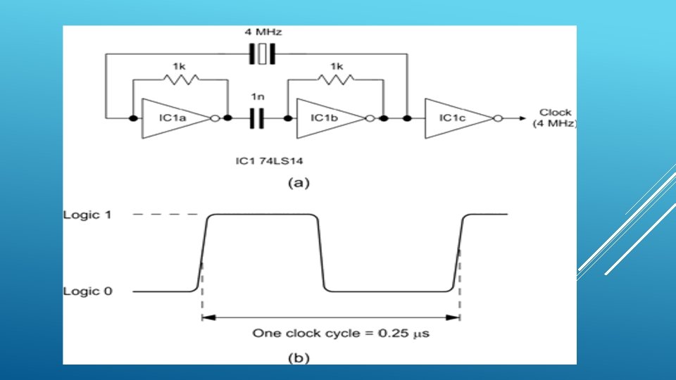
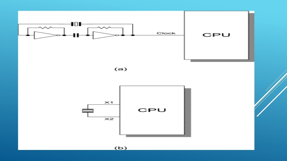
Clocks : § The clock used in a computer system is simply an accurate and stable square wave generator. § In most cases the frequency of the square wave generator is determined by a quartz crystal. § A simple 4 MHz square wave clock oscillator (together with the clock waveform that it produces) is shown in Figure 7. 2. § Note that one complete clock cycle is sometimes referred to as a T-state. Microprocessor central processing units sometimes have an internal clock circuit, in which case the quartz crystal (or other resonant device) is connected directly to pins on the microprocessor chip. § In Figure 7. 3 a an external clock is shown connected to a microprocessor, while in Figure 7. 3 b an internal clock oscillator is used.

INTERNAL ARCHITECTURE OF AN 8 -BIT PROCESSOR.

MICROPROCESSOR OPERATION § The majority of operations performed by a microprocessor involve the movement of data. Indeed, the program code (a set of instructions stored in ROM or RAM) must itself be fetched from memory prior to execution. § The microprocessor thus performs a continuous sequence of instruction fetch and execute cycles. The act of fetching an instruction code (or operand or data value) from memory involves a read operation, while the act of moving data from the microprocessor to a memory location involves a write operation (see Figure). § Each cycle of CPU operation is known as a machine cycle. Program instructions may require several machine cycles (typically between two and five). § The first machine cycle in any cycle consists of an instruction fetch (the instruction code is read from the memory) and is known as the M 1 cycle. Subsequent cycles M 2, M 3 and so on, depend on the type of instruction that is being executed. This fetch– execute sequence is shown in Figure 114.
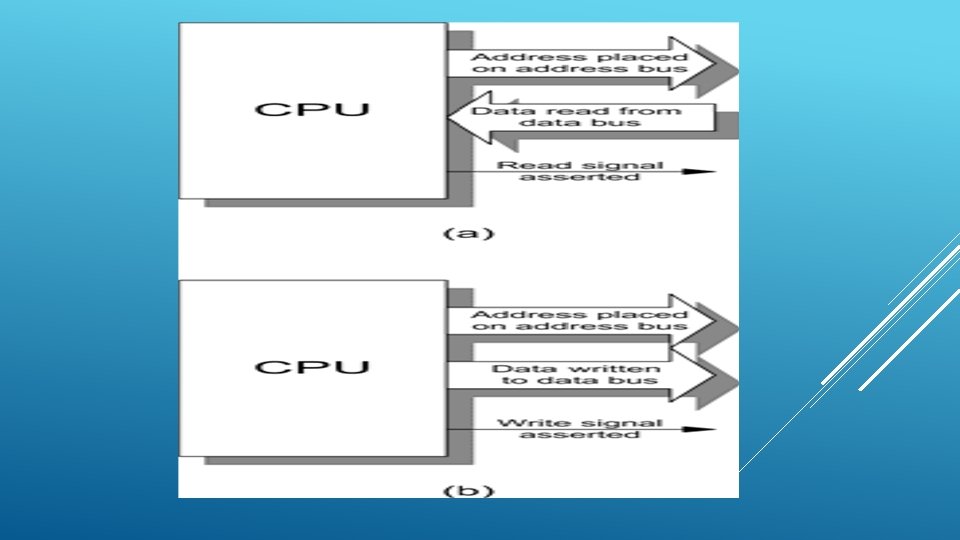

FIG. 114 A TYPICAL TIMING DIAGRAM FOR A MICROPROCESSOR CPU’S FETCH–EXECUTE CYCLE
")
MICROPROCESSOR OPERATION § Microprocessors determine the source of data (when it is being read) and the destination of data (when it is being written) by placing a unique address on the address bus. § The address at which the data is to be placed (during a write operation) or from which it is to be fetched (during a read operation) can either constitute part of the memory of the system (in which in case it may be within ROM or RAM) or it can be considered to be associated with input/output. § Since the data bus is connected to a number of VLSI devices, an essential requirement of such chips (e. g. ROM or RAM) is that their data outputs should be capable of being isolated from the bus whenever necessary. § These chips are fitted with select or enable inputs that are driven by address-decoding logic that ensures that external devices (ROM, RAM and I/O) never simultaneously attempt to place data on the bus.

MICROPROCESSOR OPERATION § The inputs of the address-decoding logic are derived from one or more of the address bus lines. § The address decoder effectively divides the available memory into blocks corresponding to a particular function (ROM, RAM, I/O, etc. ). § Hence, where the processor is reading and writing to RAM, for example, the addressdecoding logic will ensure that only the RAM is selected while the ROM and I/O remain isolated from the data bus. § Within the CPU, data is stored in several registers. Registers themselves can be thought of as a simple pigeon-hole arrangement that can store as many bits as there are holes available. § Generally, these devices can store groups of 16 or 32 bits. Additionally, some registers may be configured as either one register of 32 bits or two registers of 16 bits.

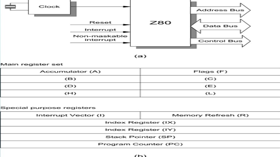
MICROPROCESSOR OPERATION § Some microprocessor registers are accessible to the programmer, whereas others are used by the microprocessor itself. § Registers may be classified as either general purpose or dedicated. In the latter case a particular function is associated with the register, such as holding the result of an operation or signaling the result of a comparison. § A basic 8 -bit microprocessor (the Z 80) and its register model is shown in Figure. This microprocessor has six general-purpose registers and that these are 8 bits in length. § The registers can also be used ‘end-on’ so that, for example, the BC register pair can be used to hold 16 -bit data. § Also the Z 80’s instruction pointer is referred to as the program counter and the status register is called the flag register. Note that different manufacturers use different names for these registers but their function remains the same.
 and logic")
ALU OPERATION § The ALU can perform arithmetic operations (addition and subtraction) and logic (complementation, logical AND, logical OR, etc. ). § The ALU operates on two inputs (8, 16, 32 or 64 bits in length, depending upon the CPU type) and it provides one output (again of 8, 16, 32 or 64 bits, depending upon the CPU type). § The ALU status is preserved in the flag register so that, for example, an overflow, zero or negative result can be detected and the necessary action can then be taken to deal with this eventuality. § A typical example might be that of a program that needs to repeat an operation a set number of times until a zero result is obtained. § The control unit is responsible for the movement of data within the CPU and the management of control signals, both internal and external. § The control unit asserts the requisite signals to read or write data as appropriate to the current instruction

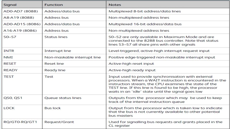
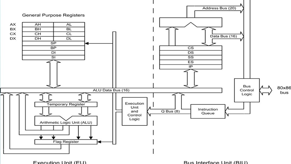
INTEL X 86 FAMILY § The original member of the x 86 family was Intel’s first true 16 -bit processor, which had 20 address lines that could directly address up to 1 MB of RAM. § The chip was available in 5, 6, 8 and 10 MHz versions. The 8086 was designed with modular internal architecture. § This approach to microprocessor design has allowed Intel to produce a similar microprocessor with identical internal architecture but employing an 8 -bit external bus. § This device, the 8088, shares the same 16 -bit internal architecture as its 16 -bit bus counterpart. Both devices were packaged in 40 -pin DIL encapsulations. § The CPU signal lines are described in Table 7. 2. The 8086/8088 can be divided internally into two functional blocks comprising an execution unit (EU) and a bus interface unit (BIU), as shown in Figure. § The EU is responsible for decoding and executing instructions, while the BIU prefetches instructions from memory and places them in an instruction queue where they await decoding and execution by the EU.

INTEL X 86 FAMILY § The EU comprises a general- and special-purpose register block, temporary registers, arithmetic logic unit (ALU), a flag (status) register and control logic. It is important to note that the principal elements of the 8086 EU remain common to each of the subsequent members of the x 86 family, but with additional registers with the more modern processors § The EU is responsible for decoding and executing instructions, while the BIU prefetches instructions from memory and places them in an instruction queue where they await decoding and execution by the EU. § The EU comprises a general- and special-purpose register block, temporary registers, arithmetic logic unit (ALU), a flag (status) register and control logic. § It is important to note that the principal elements of the 8086 EU remain common to each of the subsequent members of the x 86 family, but with additional registers with the more modern processors.

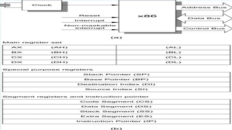
INTEL X 86 FAMILY § The BIU architecture varies according to the size of the external bus. The BIU comprises four segment registers and an instruction pointer, temporary storage for instructions held in the instruction queue, and bus control logic. § The register model and principal signals for the 8086 and x 86 processors are shown in Figure. The main registers can be used as either 8 -bit or 16 -bit registers. § The 16 -bit accumulator (register AX), for example, can be used as two 8 -bit registers (AH and AL). In this case, Intel use the ‘X’ as an abbreviation for ‘extended’, ‘H’ for ‘high’ (i. e. the high byte) and ‘L’ for ‘low’ (i. e. the low byte). § Also the use of segment registers for addressing. These registers allow the x 86 processors to address memory outside a 16 -bit address space (without these registers the processor could only address a total of 64 Kbytes of memory and I/O).

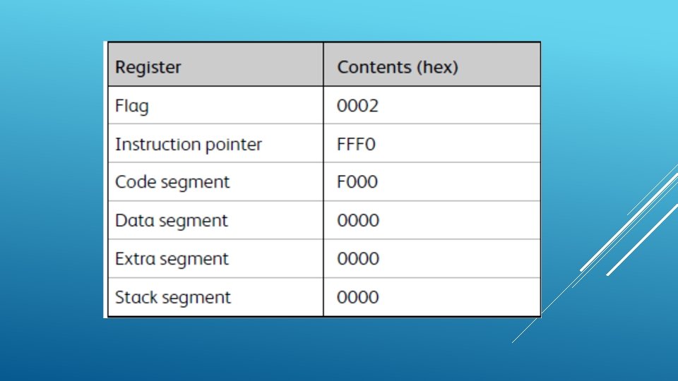
ADDRESSING § The 8086 has 20 address lines and so provides for a physical 1 MB memory address range (memory address locations 00000 to FFFFF hex). The I/O address range is 64 Kb (I/O addresses 0000 to FFFF hex). § The actual 20 -bit physical memory address is formed by shifting the segment address four zero bits to the left (adding four LSBs), which effectively multiplies the segment register contents by 16. § The contents of the instruction pointer (IP), stack pointer (SP) or other 16 -bit memory reference is then added to the result. This process is illustrated in Figure 7. 11. As an example of the process of forming a physical address reference, Table shows the state of the 8086 registers after the RESET signal is applied. § The instruction referenced (i. e. the first instruction to be executed after the RESET signal is applied) will be found by combining the instruction pointer (offset address) with the code segment register (paragraph address). § The location of the instruction referenced is FFFF 0 (i. e. F 0000 + FFF 0). Note that the PC’s ROM physically occupies addresses F 0000 to FFFFF and that, following a poweron or hardware reset, execution commences from address FFFF 0 with a jump to the initial program loader.

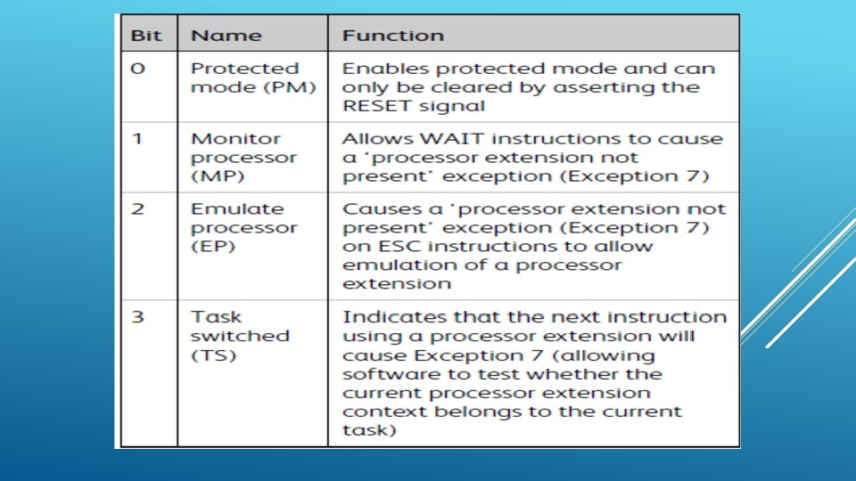
80286, 80386 AND 80486 § The 80286 offers a total physical addressing of 16 MB, but the chip also incorporates memory management capabilities that can map up to a gigabyte of virtual memory. § Depending upon the application, the 80286 is up to six times faster than the standard 5 MHz 8086 while providing upward software compatibility with the 8086 and 8088 processors. § The 80286 had 15 16 -bit registers, of which 14 are identical to those of the 8086. The additional machine status word (MSW) register controls the operating mode of the processor and also records when a task switch takes place. § The bit functions within the MSW are summarized in Table 7. 4. The MSW is initialised with a value of FFF 0 H upon reset, the remainder of the 80286 registers being initialised as shown in Table. The 80286 is packaged in a 68 -pin JEDEC type-A plastic leadless chip carrier (PLCC).
 was designed as a")
80286, 80386 AND 80486 § The 80386 (or ’ 386) was designed as a full 32 -bit device capable of manipulating data 32 bits at a time and communicating with the outside world through a 32 -bit address bus. § The 80386 offers a ‘virtual 8086’ mode of operation in which memory can be divided into 1 MB chunks with a different program allocated to each partition. The 80386 was available in two basic versions. § The 80386 SX operates internally as a 32 -bit device but presents itself to the outside world through only 16 data lines. § This has made the CPU extremely popular for use in low-cost systems which could still boast the processing power of a 80386 (despite the obvious limitation imposed by the reduced number of data lines, the ‘SX’ version of the 80386 runs at approximately 80 per cent of the speed of its fully fledged counterpart). § The 80386 comprises a bus interface unit (BIU), a code prefetch unit, an instruction decode unit, an execution unit (EU), a segmentation unit and a paging unit. § The code prefetch unit performs the program ‘lookahead’ function.

80286, 80386 AND 80486 § When the BIU is not performing bus cycles in the execution of an instruction, the code prefetch unit uses the BIU to fetch sequentially the instruction stream. § The prefetched instructions are stored in a 16 -byte ‘code queue’ where they await processing by the instruction decode unit. § The prefetch queue is fed to the instruction decode unit which translates the instructions into microcode. These micro coded instructions are then stored in a threedeep instruction queue on a first-in first-out (FIFO) basis. § This queue of instructions awaits acceptance by the EU. Immediate data and opcode offsets are also taken from the prefetch queue. § The 80486 processor was not merely an upgraded 80386 processor; its redesigned architecture offers significantly faster processing speeds when running at the same clock speed as its predecessor. §

80286, 80386 AND 80486 § Enhancements include a built-in maths coprocessor, internal cache memory and cache memory control. § The internal cache is responsible for a significant increase in processing speed. As a result, a ’ 486 operating at 25 MHz can achieve a faster processing speed than a ’ 386 operating at 33 MHz. § The ’ 486 uses a large number of additional signals associated with parity checking (PCHK) and cache operation (AHOLD, FLUSH, etc. ). § The cache comprises a set of four 2 Kb blocks (128 × 16 bytes) of high-speed internal memory. Each 16 -byte line of memory has a matching 21 -bit ‘tag’. § This tag comprises a 17 -bit linear address together with four protection bits. The cache control block contains 128 sets of seven bits. § Three of the bits are used to implement the ‘least recently used’ (LRU) system for replacement and the remaining four bits are used to indicate valid data.

INTERRUPT HANDLING § Interrupt service routines are sub-programs stored away from the main body of code that are available for execution whenever the relevant interrupt occurs. § However, since interrupts may occur at virtually any point in the execution of a main program, the response must be automatic; the processor must suspend its current task and save the return address so that the program can be resumed at the point at which it was left. § Note that the programmer must assume responsibility for preserving the state of any registers which may have their contents altered during execution of the interrupt service routine and restoring them after the interrupt has been serviced. § The Intel processor family uses a table of 256 fourbyte pointers stored in the bottom 1 Kb of memory (addresses 0000 H to 03 FFH). § Each of the locations in the interrupt pointer table can be loaded with a pointer to a different interrupt service routine. § Each pointer contains two bytes for loading into the instruction pointer (IP). This allows the programmer to place his or her interrupt service routines in any appropriate place within the 1 MB physical address space.
- Slides: 40