PROCESSORS CONTROLLERS Course code 15 EM 2202 LTP


 & Microcontroller(µC) • Microprocessor is an integrated circuit that contains all the functions")
 General-purpose microprocessor • CPU for Computers • No RAM, ROM, I/O on CPU")
 • A smaller computer • On-chip RAM, ROM, I/O ports. . . •")


 RAM (Data memory) Timers")


: – Vcc provides supply voltage to")

:reset – It is an input pin")

:External access • There is no on-chip")
:address latch enable • It is an")


 LJMP is an unconditional jump. It is a 3")


- Slides: 55
PROCESSORS & CONTROLLERS • Course code : 15 EM 2202 • L–T–P : 2– 2– 2 • Pre Requisite : 15 EC 1101 • Credits : 4
PROCESSORS AND CONTROLLERS 8086 Microprocessor: Introduction to Microprocessor, Intel Microprocessor families , 8086 Microprocessor architecture, Register Organization, Pin Description, Physical Memory Organization, Modes of operation. 8086 Instruction set & Assembly Language programming: Addressing modes, Instruction set, Assembler directives, simple Programs, Procedures and Macros, 8086 Interrupts.
PROCESSORS AND CONTROLLERS 8051 Microcontroller: Microcontroller families, 8051 Architecture, Signal Description, Register organization, Internal RAM, Special Function Registers, Interrupt control flow, Timer/Counter Operation, Serial Data Communication, and RS-232 C Standard. 8051 Programming & Interfacing: Addressing modes, Instruction set, Simple Programs involving Arithmetic and Logical Instructions, Timers/Counters, Serial Communication & Interrupts.
PROCESSORS AND CONTROLLERS PIC Microcontroller: Introduction, Architectural overview, Memory organization, interrupts and reset, I/O ports, Timers. Interfacing: Matrix Key Board, Stepper Motor, LCD’s, DAC & ADC. using 8051 and PIC Microcontroller.
Microprocessor(µP) & Microcontroller(µC) • Microprocessor is an integrated circuit that contains all the functions of a central processing unit of a computer. • Microcontroller is a control device which incorporates a microprocessor. • A system designer has to add them externally to make them functional. Application of Microprocessor includes Desktop PC's, Laptops, notepads etc. • Microcontroller has a CPU, in addition with a fixed amount of RAM, ROM and other peripherals all embedded on a single chip.
Microprocessor(µP) General-purpose microprocessor • CPU for Computers • No RAM, ROM, I/O on CPU chip itself • Example:Intel’s x 86, Motorola’s 680 x 0 CPU General. Purpose Microprocessor Many chips on mother’s board Data Bus RAM ROM I/O Port Address Bus General-Purpose Microprocessor System Timer Serial COM Port
Microcontroller(µC) • A smaller computer • On-chip RAM, ROM, I/O ports. . . • Example:Motorola’s 6811, Intel’s 8051, Zilog’s Z 8 and PIC 16 X CPU I/O Port RAM ROM Serial Timer COM Port Microcontroller A single chip
Differences between µP & µC S. No. Microprocessor Microcontroller 1 Microprocessor is heart of Computer system. Micro Controller is a heart of embedded system. 2 It is just a processor. Memory and I/O components have to be connected externally Micro controller has external processor along with internal memory and I/O components 3 Since memory and I/O has to be connected externally, the circuit becomes large. Since memory and I/O are present internally, the circuit is small. 4 Cannot be used in compact systems and hence inefficient Can be used in compact systems and hence it is an efficient technique
Differences between µP & µC S. No. Microprocessor Microcontroller 5 Cost of the entire system increases Cost of the entire system is low 6 7 Since memory and I/O Since components are internal, components are all external, each most of the operations are instruction will need external instruction, hence speed operation, hence it is relatively is fast. slower. Most of the microprocessors do not have power saving features. Most of the micro controllers have power saving modes like idle mode and power saving mode. This helps to reduce power consumption even further.
Differences between µP & µC S. No. 8 9 10 Microprocessor Microcontroller Microprocessor have less number of registers, hence more operations are memory based. Micro controller have more number of registers, hence the programs are easier to write. Microprocessors are based on von Neumann model/architecture where program and data are stored in same memory module Micro controllers are based on Harvard architecture where program memory and Data memory are separate Used mainly in washing machine, Mainly used in personal computers MP 3 players
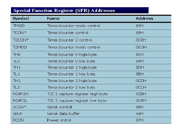
Comparison of the 8051 Family Members Feature ROM (Code memory) RAM (Data memory) Timers 8051 4 k. B 128 2 8052 8 k. B 256 3 8031 128 2 I/O Pins Serial port Interrupt 32 1 6 32 2 8 32 1 6
Block Diagram of 8051 External interrupts Interrupt Control On-chip ROM for program code Timer/Counter On-chip RAM Timer 1 Timer 0 CPU OSC Bus Control 4 I/O Ports P 0 P 1 P 2 P 3 Address/Data Serial Port Tx. D Rx. D Counter Inputs
Internal Architectural view of 8051
Pin Description of the 8051 P 1. 0 P 1. 1 P 1. 2 P 1. 3 P 1. 4 P 1. 5 P 1. 6 P 1. 7 RST (RXD)P 3. 0 (TXD)P 3. 1 (INT 0)P 3. 2 (INT 1)P 3. 3 (T 0)P 3. 4 (T 1)P 3. 5 (WR)P 3. 6 (RD)P 3. 7 XTAL 2 XTAL 1 GND 1 2 3 4 5 6 7 8 9 10 11 12 13 14 15 16 17 18 19 20 8051 (8031) 40 39 38 37 36 35 34 33 32 31 30 29 28 27 26 25 24 23 22 21 Vcc P 0. 0(AD 0) P 0. 1(AD 1) P 0. 2(AD 2) P 0. 3(AD 3) P 0. 4(AD 4) P 0. 5(AD 5) P 0. 6(AD 6) P 0. 7(AD 7) EA/VPP ALE/PROG PSEN P 2. 7(A 15) P 2. 6(A 14) P 2. 5(A 13) P 2. 4(A 12) P 2. 3(A 11) P 2. 2(A 10) P 2. 1(A 9) P 2. 0(A 8)
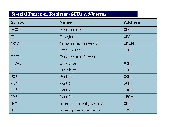
Pin Description of the 8051 • Vcc(pin 40): – Vcc provides supply voltage to the chip. – The voltage source is +5 V. • GND(pin 20):ground • XTAL 1 and XTAL 2(pins 19, 18)
Pin Description of the 8051 § Using a quartz crystal oscillator § We can observe the frequency on the XTAL 2 pin. C 2 XTAL 2 30 p. F C 1 XTAL 1 30 p. F GND
Pin Description of the 8051 • RST(pin 9):reset – It is an input pin and is active high(normally low). • The high pulse must be high at least 2 machine cycles. – It is a power-on reset. • Upon applying a high pulse to RST, the microcontroller will reset and all values in registers will be lost. • Reset values of some 8051 registers
Pin Description of the 8051 Vcc + 10 u. F 31 30 p. F 8. 2 K 30 p. F 11. 0592 MHz 19 18 EA/VPP X 1 X 2 9 RST
Pin Description of the 8051 • /EA(pin 31):External access • There is no on-chip ROM in 8031 and 8032. • The /EA pin is connected to GND to indicate the code is stored externally. • /PSEN & ALE are used for external ROM. • For 8051, /EA pin is connected to Vcc. • “/” means active low. • /PSEN(pin 29):program store enable • This is an output pin and is connected to the OE pin of the ROM.
Pin Description of the 8051 • ALE(pin 30):address latch enable • It is an output pin and is active high. • 8051 port 0 provides both address and data. • The ALE pin is used for de-multiplexing the address and data by connecting to the G pin of the 74 LS 373 latch. • I/O port pins • The four ports P 0, P 1, P 2, and P 3. • Each port uses 8 pins. • All I/O pins are bi-directional.
Pin Description of the 8051 • The 8051 has four I/O ports – Port 0 (pins 32 -39):P 0(P 0. 0~P 0. 7) – Port 1(pins 1 -8) :P 1(P 1. 0~P 1. 7) – Port 2(pins 21 -28):P 2(P 2. 0~P 2. 7) – Port 3(pins 10 -17):P 3(P 3. 0~P 3. 7) – Each port has 8 pins. • Ex:P 0. 0 is the bit 0 (LSB) of P 0 • Ex:P 0. 7 is the bit 7 (MSB)of P 0 • These 8 bits form a byte. • Each port can be used as input or output (bi-direction).
Pin Description of the 8051 • Each pin of I/O ports – Internal CPU bus:communicate with CPU – A D latch store the value of this pin • D latch is controlled by “Write to latch” – Write to latch= 1:write data into the D latch – 2 Tri-state buffer. • TB 1: controlled by “Read pin” – Read pin= 1:read the data present at the pin • TB 2: controlled by “Read latch” – Read latch= 1:read value from internal latch – A transistor M 1 gate • Gate=0: open • Gate=1: close
Port 0 with Pull-Up Resistors Vcc Port 0 P 0. 0 DS 5000 P 0. 1 P 0. 2 8751 P 0. 3 P 0. 4 8951 P 0. 5 P 0. 6 P 0. 7 10 K
Port 3 Alternate Functions P 3 Bit Function Pin P 3. 0 P 3. 1 P 3. 2 P 3. 3 P 3. 4 P 3. 5 P 3. 6 P 3. 7 Rx. D Tx. D INT 0 INT 1 T 0 T 1 WR RD 10 11 12 13 14 15 16 17
RESET Value of Some 8051 Registers Register PC ACC B PSW SP DPTR RAM are all zero. Reset Value 0000 00 07 0000
Memory mapping in 8051 • ROM memory map in 8051 family 4 k 0000 H 8 k 32 k 0000 H 0 FFFH DS 5000 -32 8751 AT 89 C 51 1 FFFH from Atmel Corporation 8752 AT 89 C 52 7 FFFH from Dallas Semiconductor
Registers A B R 0 DPH DPL DPTR R 1 R 2 PC R 3 R 4 R 5 R 6 R 7 Some 8 -bit Registers of the 8051 Some 8051 16 -bit Register PC
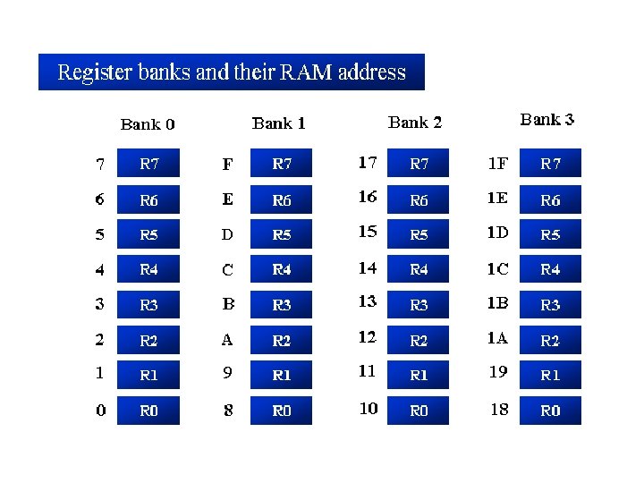
RAM memory space allocation in the 8051 7 FH Scratch pad RAM 30 H 2 FH Bit-Addressable RAM 20 H 1 FH Register Bank 3 18 H 17 H Register Bank 2 10 H 0 FH (Stack) Register Bank 1 08 H 07 H Register Bank 0 00 H
Bit-Addressable RAM
8051 Flag bits and the PSW register CY AC F 0 RS 1 RS 0 OV -- P CYPSW. 7 Carry flag ACPSW. 6 Auxiliary carry flag --PSW. 5 Available to the user for general purpose RS 1 PSW. 4 Register Bank selector bit 1 RS 0 PSW. 3 Register Bank selector bit 0 OVPSW. 2 Overflow flag --PSW. 1 User define bit PPSW. 0 Parity flag Set/Reset odd/even parity RS 1 RS 0 Register Bank Address 0 00 H-07 H 0 1 1 08 H-0 FH 1 0 2 10 H-17 H 1 1 3 18 H-1 FH
Stack in the 8051 The register used to access the stack is called SP (stack pointer) register. 7 FH Scratch pad RAM 30 H 2 FH Bit-Addressable RAM The stack pointer in the 8051 is only 8 bits wide, which means that it can take value 00 to FFH. When 8051 powered up, the SP register contains value 07. 20 H 1 FH 18 H 17 H 10 H 0 FH 08 H 07 H 00 H Register Bank 3 Register Bank 2 (Stack) Register Bank 1 Register Bank 0
Example of STACK operation: MOV MOV PUSH R 6, #25 H R 1, #12 H R 4, #0 F 3 H 6 1 4 0 BH 0 BH 0 AH 0 AH F 3 09 H 09 H 12 08 H 08 H 25 Start SP=07 H 25 SP=08 H SP=09 H SP=0 AH
Addressing Modes Immediate Register Direct Register Indirect Indexed
Immediate Addressing Mode MOV A, #65 H MOV A, #’A’ MOV R 6, #65 H MOV DPTR, #2343 H MOV P 1, #65 H
Register Addressing Mode MOV ADD MOV MOV Rn, A A, Rn DPL, R 6 DPTR, A Rm, Rn ; n=0, . . , 7
Direct Addressing Mode Although the entire of 128 bytes of RAM can be accessed using direct addressing mode, it is most often used to access RAM loc. 30 – 7 FH. MOV MOV R 0, 40 H 56 H, A A, 4 6, 2 ; ≡ MOV A, R 4 ; copy R 2 to R 6 ; MOV R 6, R 2 is invalid ! SFR register and their address MOV MOV 0 E 0 H, #66 H 0 F 0 H, R 2 80 H, A ; ≡ MOV A, #66 H ; ≡ MOV B, R 2 ; ≡ MOV P 1, A
Register Indirect Addressing Mode In this mode, register is used as a pointer to the data. MOV A, @Ri MOV @R 1, B ; move content of RAM loc. Where address is held by Ri into A ( i=0 or 1 ) In other word, the content of register R 0 or R 1 is sources or target in MOV, ADD and SUBB instructions. Example: Write a program to copy a block of 10 bytes from RAM location starting at 40 H to RAM location starting at 60 H. Solution: BACK: MOV R 0, #40 H MOV R 1, #60 H MOV R 2, #10 MOV A, @R 0 MOV @R 1, A INC R 0 INC R 1 DJNZ R 2, BACK ; source pointer ; destination pointer ; counter
Indexed Addressing Mode And On-Chip ROM Access This mode is widely used in accessing data elements of look-up table entries located in the program (code) space ROM at the 8051 MOVC A, @A+DPTR A= content of address A +DPTR from ROM Note: Because the data elements are stored in the program (code ) space ROM of the 8051, it uses the instruction MOVC instead of MOV. The “C” means code.
SJMP and LJMP: LJMP(long jump) LJMP is an unconditional jump. It is a 3 -byte instruction in which the first byte is the op-code, and the second and third bytes represent the 16 -bit address of the target location. The 20 byte target address allows a jump to any memory location from 0000 to FFFFH. SJMP(short jump) In this 2 -byte instruction. The first byte is the op-code and the second byte is the relative address of the target location. The relative address range of 00 -FFH is divided into forward and backward jumps, that is , within -128 to +127 bytes of memory relative to the address of the current PC.
MUL & DIV MUL AB MOV A, #25 H MOV B, #65 H MUL AB DIV AB MOV A, #25 H MOV B, #10 H DIV AB ; B|A = A*B ; 25 H*65 H=0 E 99 ; B=0 EH, A=99 H ; A = A/B, B = A mod B ; A=2, B=5
Rotate EXAMPLE: RRC: C RL: RLC: C
8051 INSTRUCTION SET ACALL: Absolute Call JC: Jump if Carry Set PUSH: Push Value Onto Stack ADD, ADDC: Add Acc. (With Carry) JMP: Jump to Address RET: Return From Subroutine AJMP: Absolute Jump JNB: Jump if Bit Not Set RETI: Return From Interrupt ANL: Bitwise AND JNC: Jump if Carry Not Set RL: Rotate Accumulator Left CJNE: Compare & Jump if Not Equal JNZ: Jump if Acc. Not Zero RLC: Rotate Acc. Left Through Carry CLR: Clear Register JZ: Jump if Accumulator Zero RR: Rotate Accumulator Right CPL: Complement Register LCALL: Long Call RRC: Rotate Acc. Right Through Carry DA: Decimal Adjust LJMP: Long Jump SETB: Set Bit DEC: Decrement Register MOV: Move Memory SJMP: Short Jump DIV: Divide Accumulator by B MOVC: Move Code Memory SUBB: Sub. From Acc. With Borrow DJNZ: Dec. Reg. & Jump if Not Zero MOVX: Move Extended Memory SWAP: Swap Accumulator Nibbles INC: Increment Register MUL: Multiply Accumulator by B XCH: Exchange Bytes JB: Jump if Bit Set NOP: No Operation XCHD: Exchange Digits JBC: Jump if Bit Set and Clear Bit ORL: Bitwise OR XRL: Bitwise Exclusive OR POP: Pop Value From Stack Undefined: Undefined Instruction
Arithmetic instructions: ADD A, Rn ADD A, Direct ADD A, @Ri SUBB A, Direct SUBB A, @Ri SUBB A, #Data ADD A, #Data INC A ADDC A, Rn ADDC A, Direct ADDC A, @Ri ADDC A, #Data SUBB A, Rn INC Direct INC @Ri DEC A DEC Rn
Arithmetic instructions: DEC Direct DEC @Ri INC DPTR MUL AB DIV AB DA A
Logical instructions: ANL A, Rn ANL A, Direct ANL A, @Ri ORL A, #Data ORL Direct, A ORL Direct, #Data ANL A, #Data XRL A, Rn ANL Direct, A ANL Direct, #Data ORL A, Rn ORL A, Direct ORL A, @Ri XRL A, Direct XRL A, @Ri XRL A, #Data XRL Direct, A XRL Direct, #Data
Logical instructions: CLR A CPL A RLC A RRC A SWAP A
Data transfer instructions: MOV A, Rn MOV A, Direct MOV A, @Ri MOV Direct, Direct MOV Direct, @Ri MOV Direct, #Data MOV A, #Data MOV @Ri, A MOV Rn, Direct MOV Rn, #Data MOV Direct, A MOV Direct, Rn MOV @Ri, Direct MOV @Ri, #Data MOV DPTR, #Data 16 MOVX A, @Ri MOVX A, @DPTR
Data transfer instructions: PUSH Direct POP Direct XCH A, Rn XCH A, Direct XCH A, @Ri XCHD A, @Ri MOVX @Ri, A MOV @DPTR, A
Boolean Variable Manipulation instructions: CLR C CLR bit SETB C ORL C, /bit MOV C, bit MOV bit, C SETB bit JC rel CPL C CPL bit ANL C, /bit ORL C, bit JNC rel JB bit, rel JNB bit, rel JBC bit, rel
Program branching instructions: ACALL addr 11 LCALL addr 16 RET JNZ rel CJNE A, direct, rel CJNE A, #data, rel RETI CJNE Rn, #data, rel AJMP addr 11 LJMP addr 16 SJMP rel JMP @A+DPTR JZ rel CJNE @Ri, #data, rel DJNZ Rn, rel DJNZ direct, rel NOP
END