Chapter 7 ADC DAC and Sensor Interfacing 1

- Slides: 39

Chapter 7 ADC, DAC, and Sensor Interfacing 1

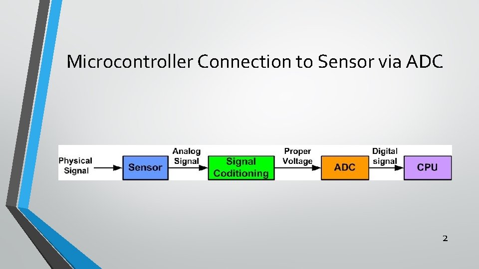
Microcontroller Connection to Sensor via ADC 2

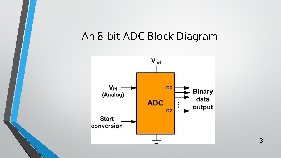
An 8 -bit ADC Block Diagram 3

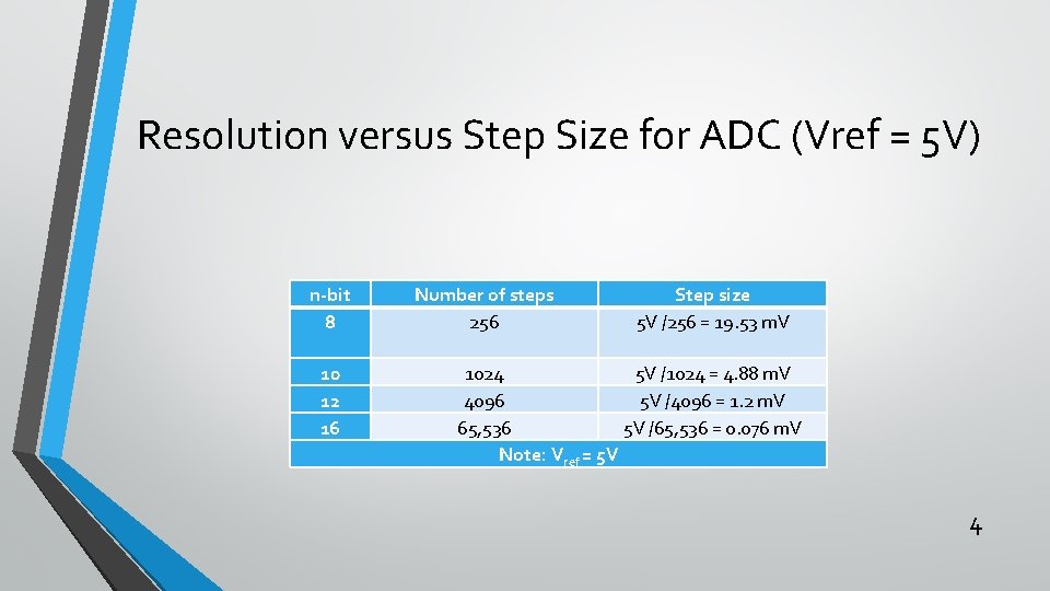
Resolution versus Step Size for ADC (Vref = 5 V) n-bit 8 10 12 16 Number of steps 256 Step size 5 V /256 = 19. 53 m. V 1024 5 V /1024 = 4. 88 m. V 4096 5 V /4096 = 1. 2 m. V 65, 536 5 V /65, 536 = 0. 076 m. V Note: Vref = 5 V 4

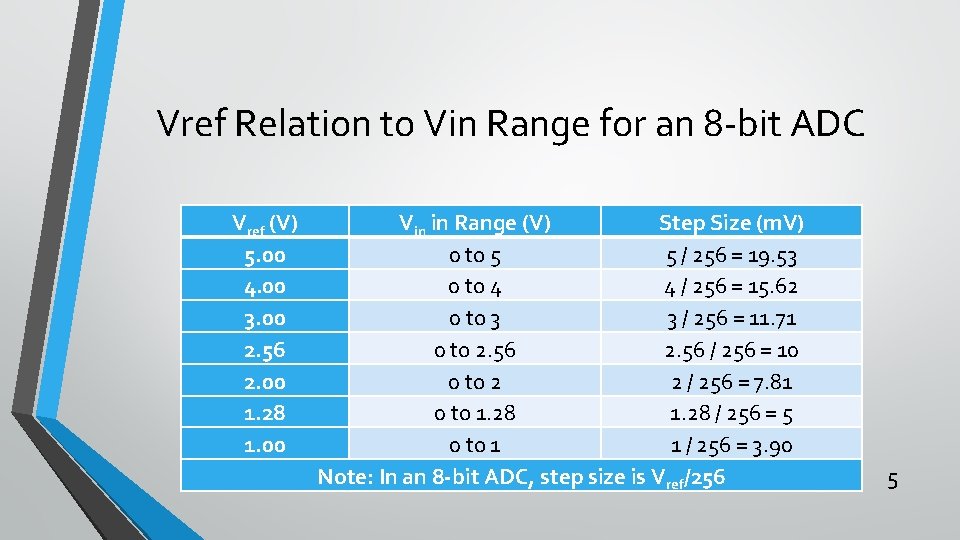
Vref Relation to Vin Range for an 8 -bit ADC Vref (V) 5. 00 4. 00 3. 00 2. 56 2. 00 1. 28 1. 00 Vin in Range (V) Step Size (m. V) 0 to 5 5 / 256 = 19. 53 0 to 4 4 / 256 = 15. 62 0 to 3 3 / 256 = 11. 71 0 to 2. 56 / 256 = 10 0 to 2 2 / 256 = 7. 81 0 to 1. 28 / 256 = 5 0 to 1 1 / 256 = 3. 90 Note: In an 8 -bit ADC, step size is Vref/256 5

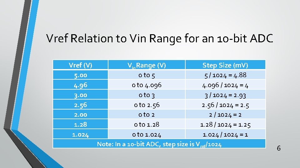
Vref Relation to Vin Range for an 10 -bit ADC Vref (V) 5. 00 4. 96 3. 00 2. 56 2. 00 1. 28 1. 024 Vin. Range (V) Step Size (m. V) 0 to 5 5 / 1024 = 4. 88 0 to 4. 096 / 1024 = 4 0 to 3 3 / 1024 = 2. 93 0 to 2. 56 / 1024 = 2. 5 0 to 2 2 / 1024 = 2 0 to 1. 28 / 1024 = 1. 25 0 to 1. 024 / 1024 = 1 Note: In a 10 -bit ADC, step size is Vref/1024 6

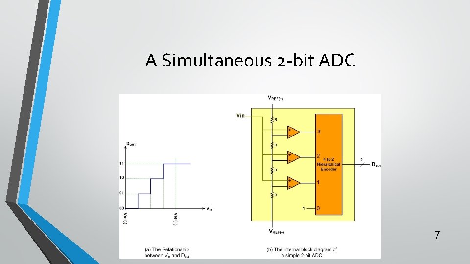
A Simultaneous 2 -bit ADC 7

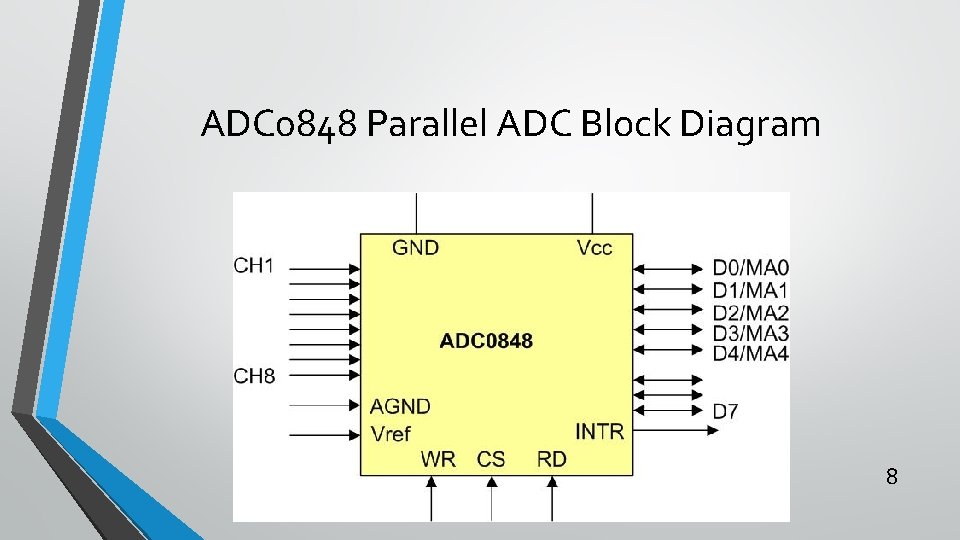
ADC 0848 Parallel ADC Block Diagram 8

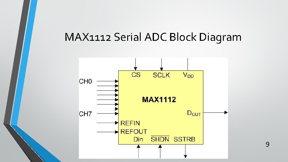
MAX 1112 Serial ADC Block Diagram 9

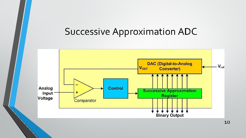
Successive Approximation ADC 10

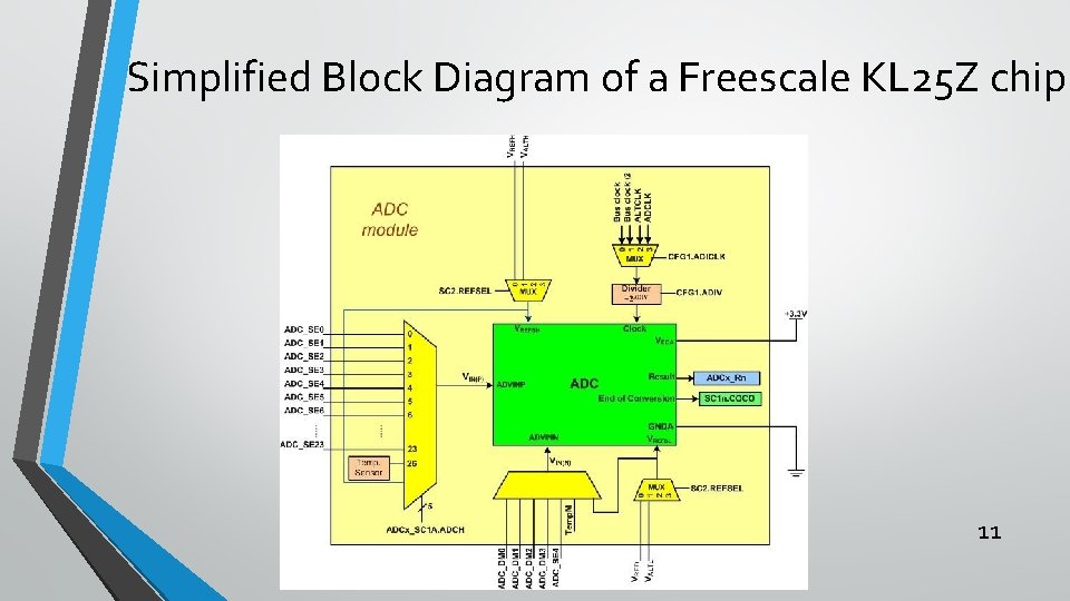
Simplified Block Diagram of a Freescale KL 25 Z chip 11

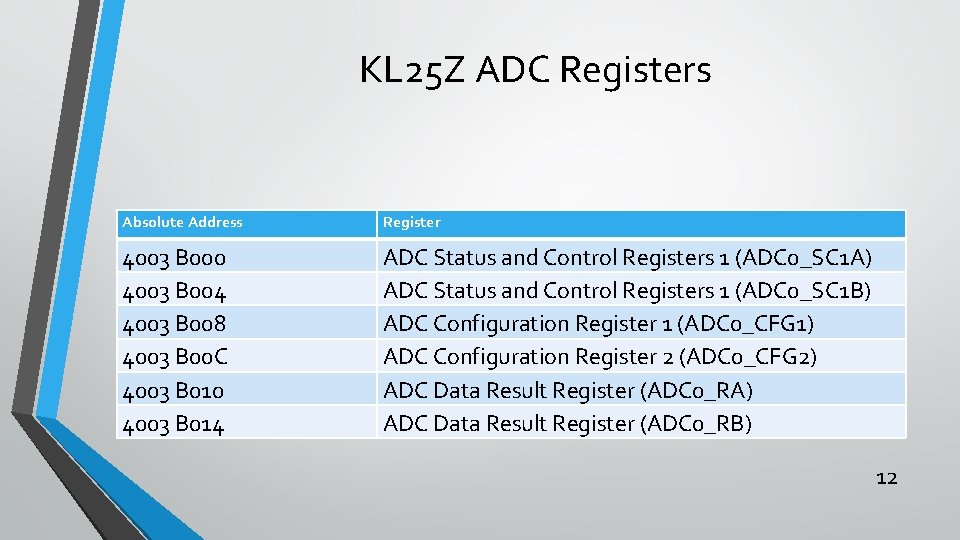
KL 25 Z ADC Registers Absolute Address Register 4003 B 000 4003 B 004 4003 B 008 4003 B 00 C 4003 B 010 4003 B 014 ADC Status and Control Registers 1 (ADC 0_SC 1 A) ADC Status and Control Registers 1 (ADC 0_SC 1 B) ADC Configuration Register 1 (ADC 0_CFG 1) ADC Configuration Register 2 (ADC 0_CFG 2) ADC Data Result Register (ADC 0_RA) ADC Data Result Register (ADC 0_RB) 12

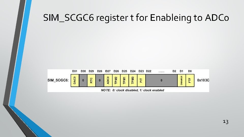
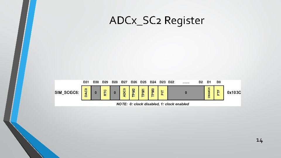
SIM_SCGC 6 register t for Enableing to ADC 0 13

ADCx_SC 2 Register 14

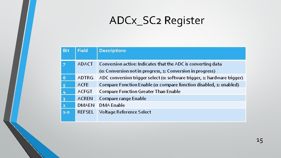
ADCx_SC 2 Register Bit Field 7 ADACT 6 5 4 3 2 1 -0 Descriptions Conversion active: Indicates that the ADC is converting data (0: Conversion not in progress, 1: Conversion in progress) ADTRG ADC conversion trigger select (0: software trigger, 1: hardware trigger) ACFE Compare Function Enable (0: compare function disabled, 1: enabled) ACFGT Compare Function Greater Than Enable ACREN Compare range Enable DMAEN DMA Enable REFSEL Voltage Reference Select 15

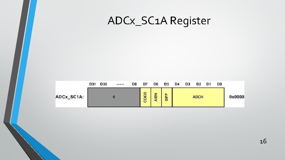
ADCx_SC 1 A Register 16

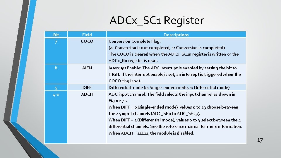
ADCx_SC 1 Register Bit 7 Field COCO 6 AIEN 5 4 -0 DIFF ADCH Descriptions Conversion Complete Flag: (0: Conversion is not completed, 1: Conversion is completed) The COCO is cleared when the ADCx_SC 1 n register is written or the ADCx_Rn register is read. Interrupt Enable: The ADC interrupt is enabled by setting the bit to HIGH. If the interrupt enable is set, an interrupt is triggered when the COCO flag is set. Differential mode (0: Single-ended mode, 1: Differential mode) ADC input channel: The field selects the input channel as shown in Figure 7 -7. When DIFF = 0 (single-ended mode), values 0 to 23 choose between the 24 input channels (ADC_SE 0 to ADC_SE 23). When DIFF = 1 (Differential mode), values 0 to 3 select between the 4 differential channels. See the reference manual for more information. When ADCH = 11111, the module is disabled. 17

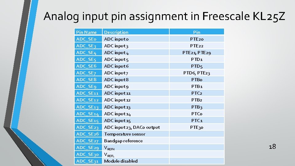
Analog input pin assignment in Freescale KL 25 Z Pin Name ADC_SE 0 ADC_SE 3 ADC_SE 4 ADC_SE 5 ADC_SE 6 ADC_SE 7 ADC_SE 8 ADC_SE 9 ADC_SE 11 ADC_SE 12 ADC_SE 13 ADC_SE 14 ADC_SE 15 ADC_SE 23 ADC_SE 26 ADC_SE 27 ADC_SE 29 ADC_SE 30 ADC_SE 31 Description ADC input 0 ADC input 3 ADC input 4 ADC input 5 ADC input 6 ADC input 7 ADC input 8 ADC input 9 ADC input 11 ADC input 12 ADC input 13 ADC input 14 ADC input 15 ADC input 23, DAC 0 output Temperature sensor Bandgap reference VREFH VREFL Module disabled Pin PTE 20 PTE 22 PTE 21, PTE 29 PTD 1 PTD 5 PTD 6, PTE 23 PTB 0 PTB 1 PTC 2 PTB 3 PTC 0 PTC 1 PTE 30 18

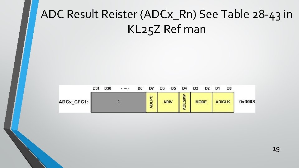
ADC Result Reister (ADCx_Rn) See Table 28 -43 in KL 25 Z Ref man 19

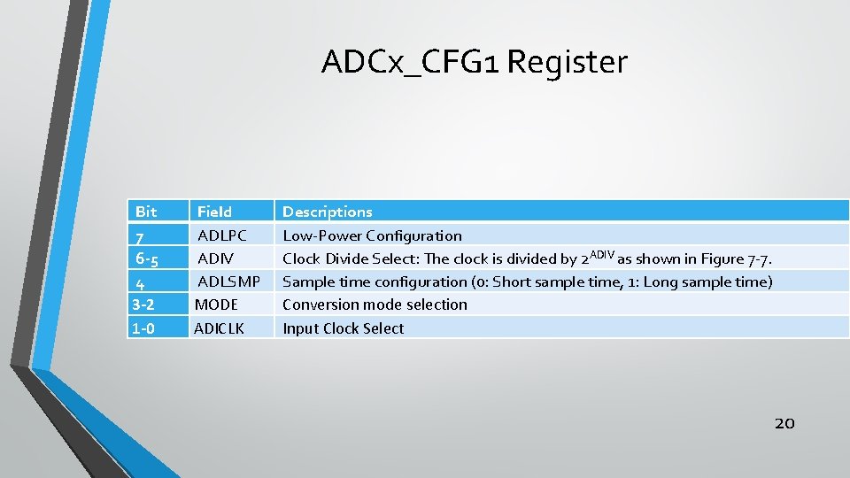
ADCx_CFG 1 Register Bit 7 6 -5 4 3 -2 1 -0 Field ADLPC ADIV ADLSMP MODE ADICLK Descriptions Low-Power Configuration Clock Divide Select: The clock is divided by 2 ADIV as shown in Figure 7 -7. Sample time configuration (0: Short sample time, 1: Long sample time) Conversion mode selection Input Clock Select 20

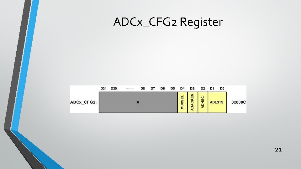
ADCx_CFG 2 Register 21

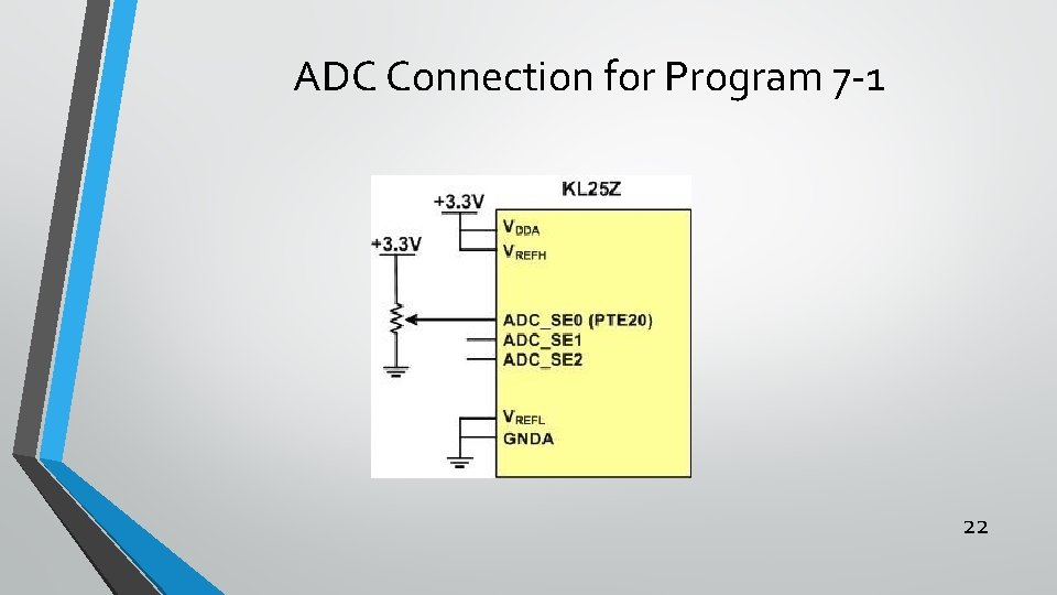
ADC Connection for Program 7 -1 22

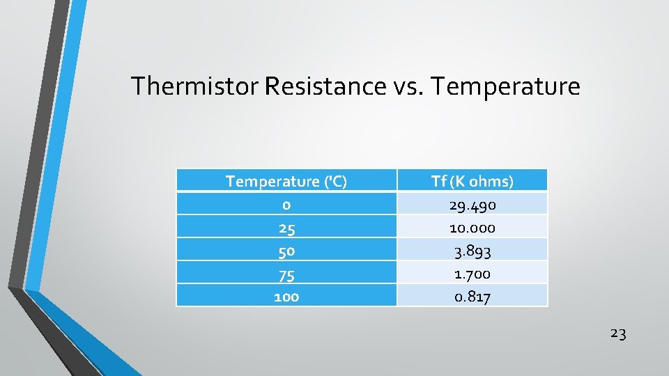
Thermistor Resistance vs. Temperature ('C) 0 25 50 75 100 Tf (K ohms) 29. 490 10. 000 3. 893 1. 700 0. 817 23

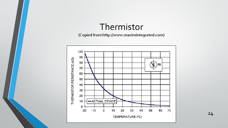
Thermistor (Copied from http: //www. maximintegrated. com) 24

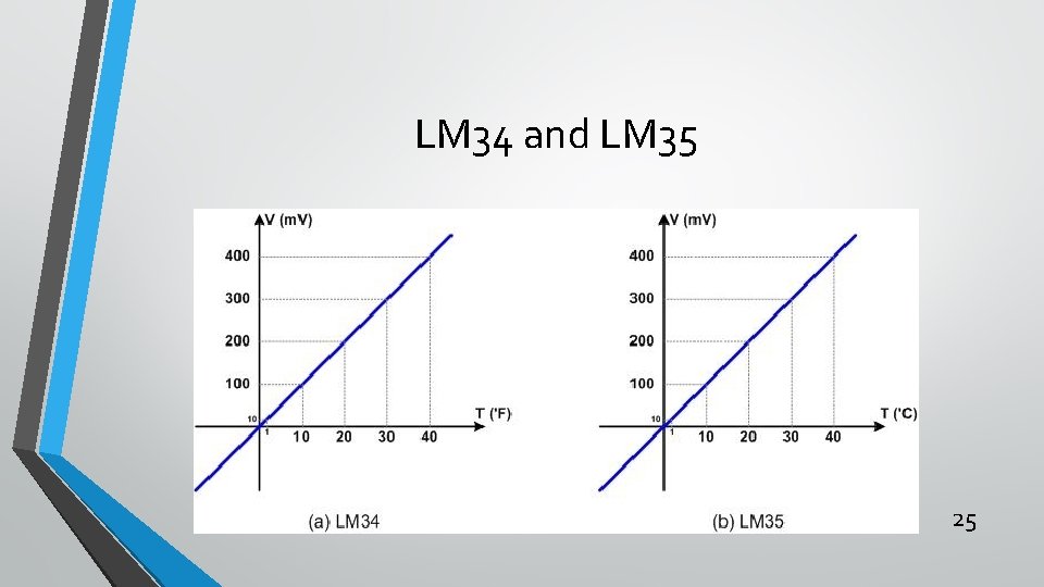
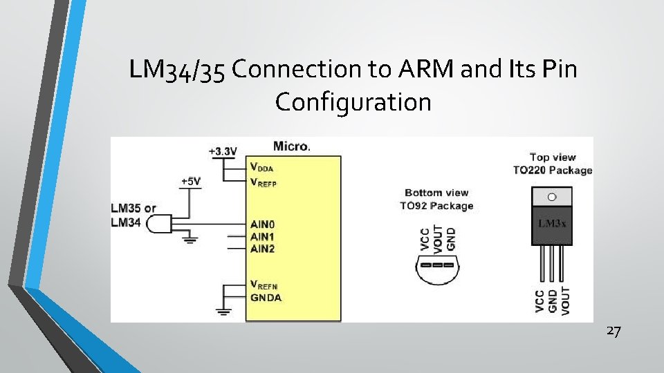
LM 34 and LM 35 25

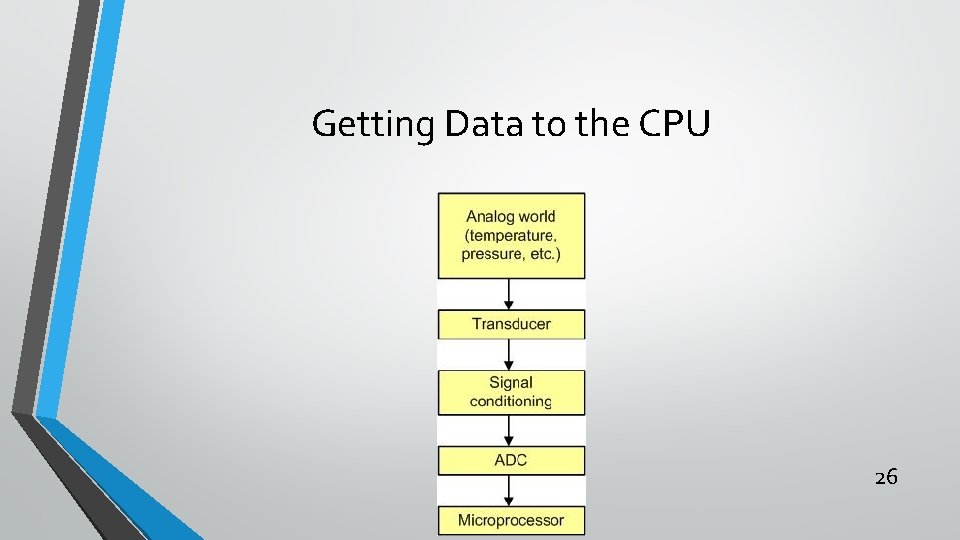
Getting Data to the CPU 26

LM 34/35 Connection to ARM and Its Pin Configuration 27

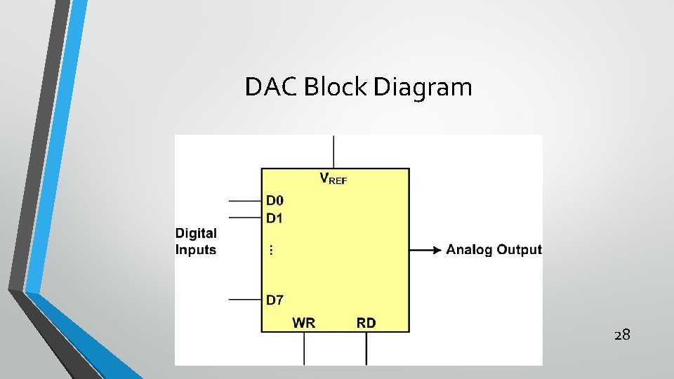
DAC Block Diagram 28

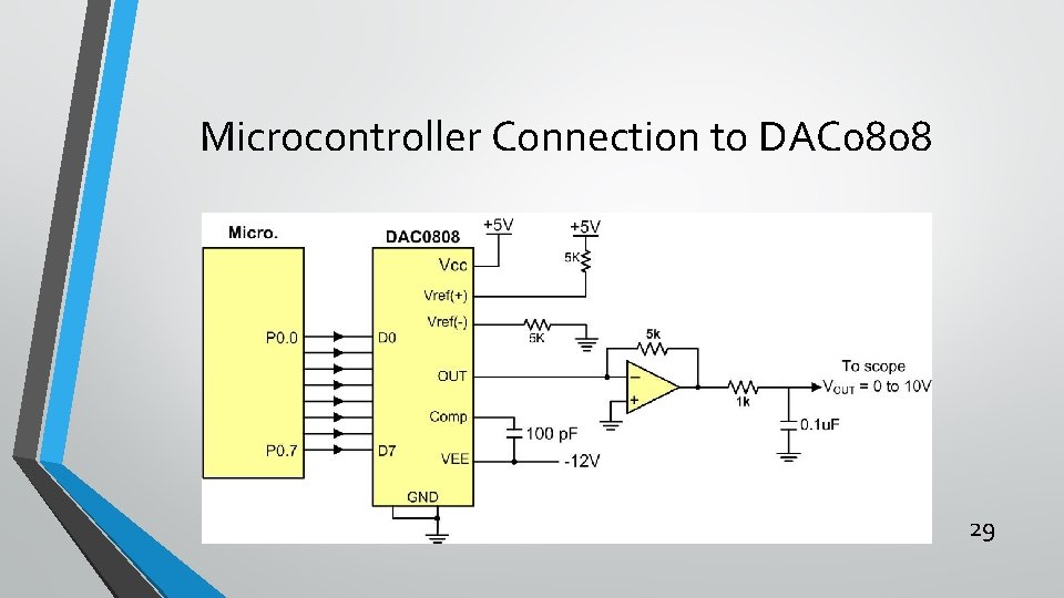
Microcontroller Connection to DAC 0808 29

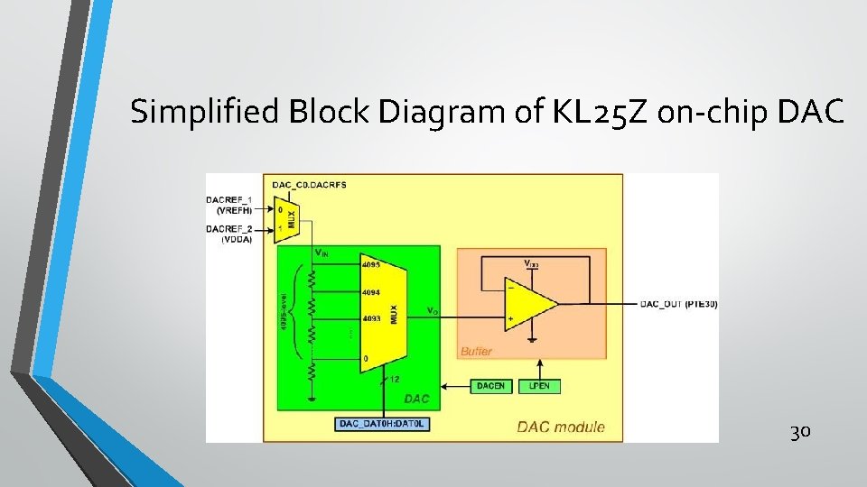
Simplified Block Diagram of KL 25 Z on-chip DAC 30

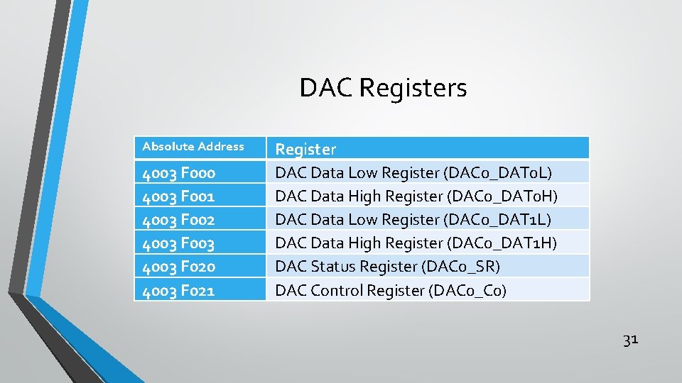
DAC Registers Absolute Address 4003 F 000 4003 F 001 4003 F 002 4003 F 003 4003 F 020 4003 F 021 Register DAC Data Low Register (DAC 0_DAT 0 L) DAC Data High Register (DAC 0_DAT 0 H) DAC Data Low Register (DAC 0_DAT 1 L) DAC Data High Register (DAC 0_DAT 1 H) DAC Status Register (DAC 0_SR) DAC Control Register (DAC 0_C 0) 31

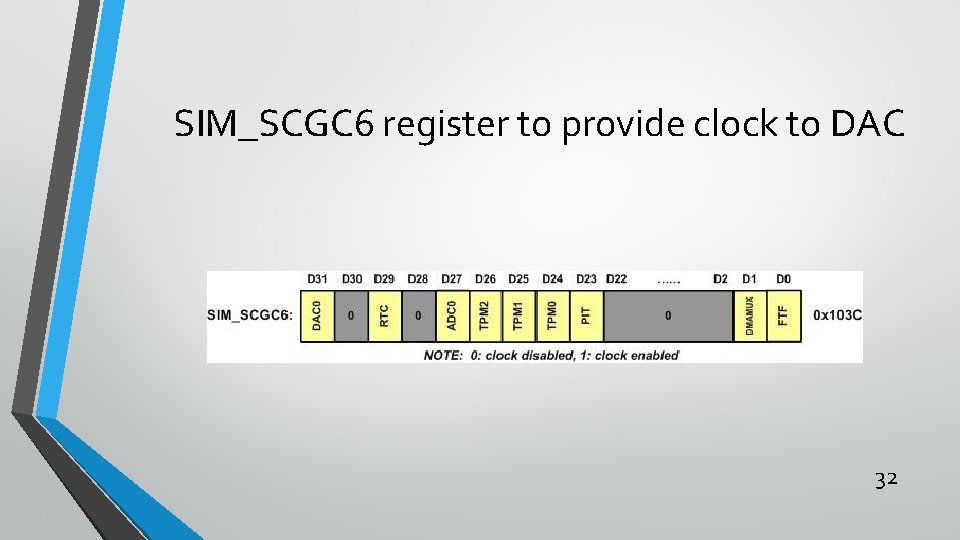
SIM_SCGC 6 register to provide clock to DAC 32

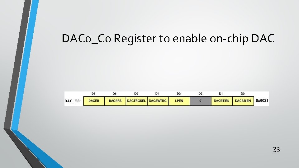
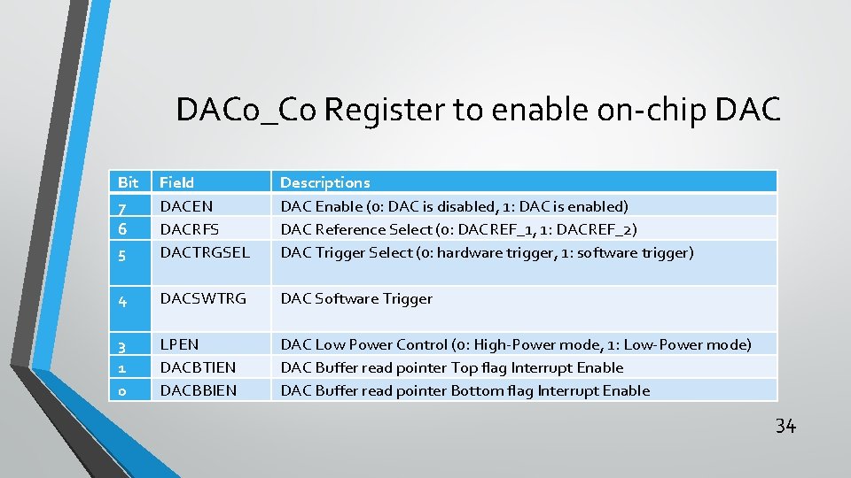
DAC 0_C 0 Register to enable on-chip DAC 33

DAC 0_C 0 Register to enable on-chip DAC Bit 7 6 5 Field DACEN DACRFS DACTRGSEL Descriptions DAC Enable (0: DAC is disabled, 1: DAC is enabled) DAC Reference Select (0: DACREF_1, 1: DACREF_2) DAC Trigger Select (0: hardware trigger, 1: software trigger) 4 DACSWTRG DAC Software Trigger 3 1 0 LPEN DACBTIEN DACBBIEN DAC Low Power Control (0: High-Power mode, 1: Low-Power mode) DAC Buffer read pointer Top flag Interrupt Enable DAC Buffer read pointer Bottom flag Interrupt Enable 34

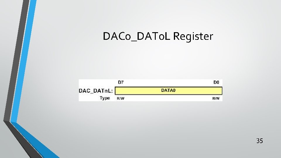
DAC 0_DAT 0 L Register 35

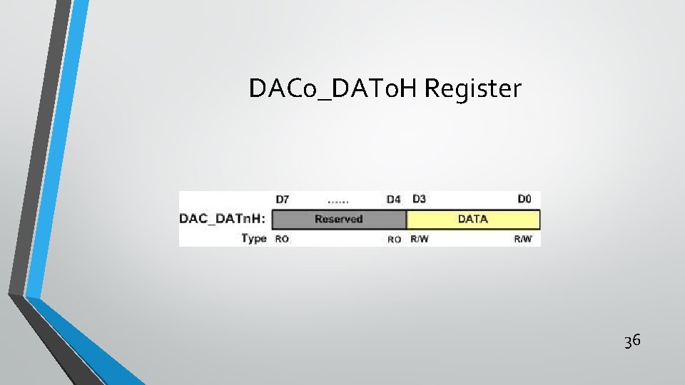
DAC 0_DAT 0 H Register 36

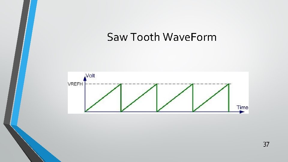
Saw Tooth Wave. Form 37

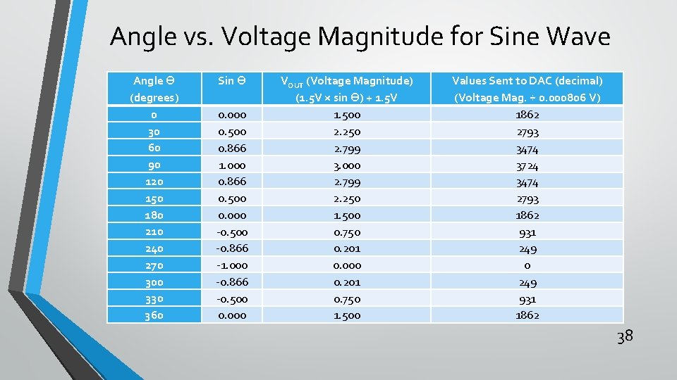
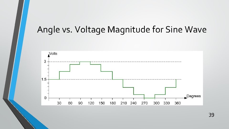
Angle vs. Voltage Magnitude for Sine Wave Angle Ɵ (degrees) 0 30 60 90 120 150 180 210 240 270 300 330 360 Sin Ɵ 0. 000 0. 500 0. 866 1. 000 0. 866 0. 500 0. 000 -0. 500 -0. 866 -1. 000 -0. 866 -0. 500 0. 000 VOUT (Voltage Magnitude) (1. 5 V × sin Ɵ) + 1. 5 V 1. 500 2. 250 2. 799 3. 000 2. 799 2. 250 1. 500 0. 750 0. 201 0. 000 0. 201 0. 750 1. 500 Values Sent to DAC (decimal) (Voltage Mag. ÷ 0. 000806 V) 1862 2793 3474 3724 3474 2793 1862 931 249 0 249 931 1862 38

Angle vs. Voltage Magnitude for Sine Wave 39