1262022 Ravindra College of Engineering for Women Chapter


- Slides: 147

1/26/2022 Ravindra College of Engineering for Women

Chapter 7 FEATURES AND INTERFACING OF PROGRAMMABLE DEVICES FOR 8086 -BASED SYSTEMS 1/26/2022 Ravindra College of Engineering for Women

Intel 8255 PPI • Intel microprocessors can transfer data between external devices such as input and output devices through ports. • In normal conditions a register can act as an I/O port. However, having a separate register and configuring it for input and output operation becomes difficult and tedious. • Intel has designed a separate IC 8255 with the objective of interfacing input and output devices with Intel microprocessors. © Oxford University Press 2013. All rights reserved.

Intel 8255 PPI • 8255 is used on a range of several I/O cards that plug into available slots in the personal computer (PC). • This chip can perform both digital input and output (DIO) operations from the processor in a preprogrammed manner. © Oxford University Press 2013. All rights reserved.

8255 – common applications • Turning on or off an electronic switch such as a bipolar junction transistor (BJT), a metal oxide semiconductor field effect transistor (MOSFET), or an insulated gate bipolar transistor (IGBT). • Controlling movement by use of DC/AC/stepper motors • Detecting the position using proximity sensors and interfacing different sensors (temperature, flow, pressure or level, etc. ) through an analog to digital converter (ADC) © Oxford University Press 2013. All rights reserved.

8255 – common features • Three 8 -bit ports named as A, B, and C are present. • Port C has been divided to two groups of 4 bits each as port C upper (PCU) and port C lower (PCL). Each of them can be programmed independently for input and output operation. • All the ports can be programmed for simple I/O or handshake I/O for the data transfer in I/O modes. © Oxford University Press 2013. All rights reserved.

8255 – common features • Each port C bit can be set/reset individually in bit set/reset (BSR) mode. • Port A bits and PCU bits are grouped as group A (GA). • Port B bits and PCL bits are grouped as group B (GB). © Oxford University Press 2013. All rights reserved.

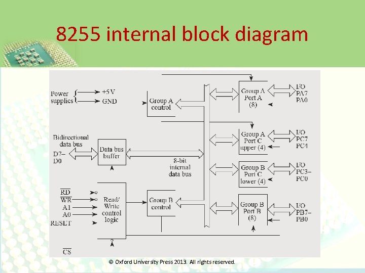
8255 internal block diagram © Oxford University Press 2013. All rights reserved.

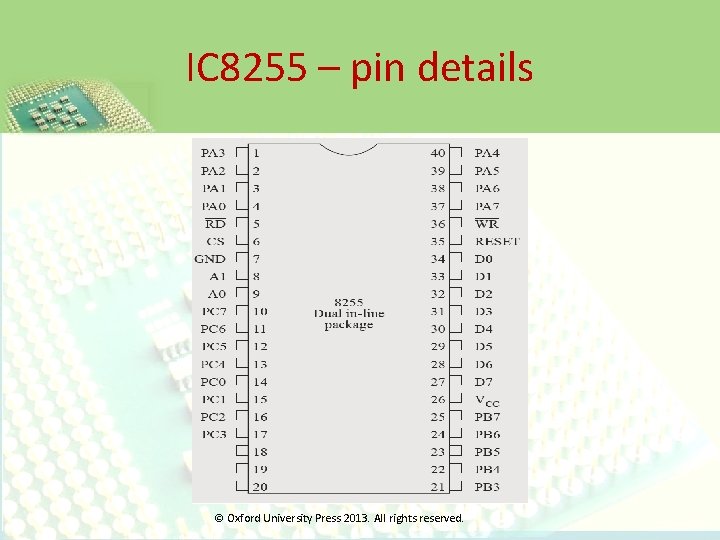
IC 8255 – pin details © Oxford University Press 2013. All rights reserved.

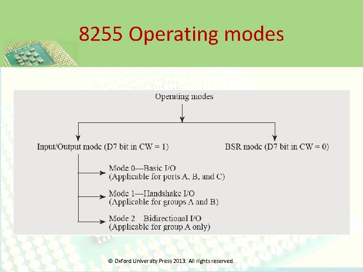
8255 Operating modes © Oxford University Press 2013. All rights reserved.

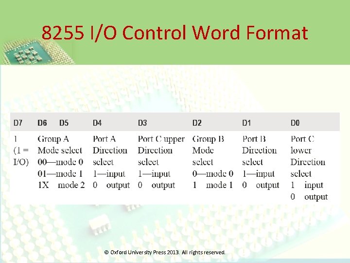
8255 I/O Control Word Format © Oxford University Press 2013. All rights reserved.

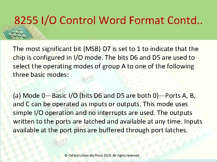
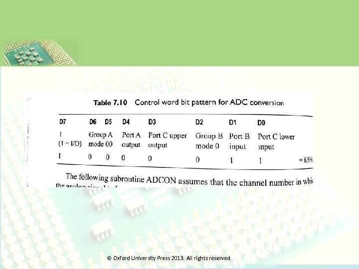
8255 I/O Control Word Format Contd. . The most significant bit (MSB) D 7 is set to 1 to indicate that the chip is configured in I/O mode. The bits D 6 and D 5 are used to select the operating modes of group A to one of the following three basic modes: (a) Mode 0—Basic I/O (bits D 6 and D 5 are both 0)—Ports A, B, and C can be operated as inputs or outputs. This mode uses simple I/O operation and no interrupts are used. The outputs written to the ports are latched and available at any time. Inputs available at the port pins are buffered through port latches. © Oxford University Press 2013. All rights reserved.

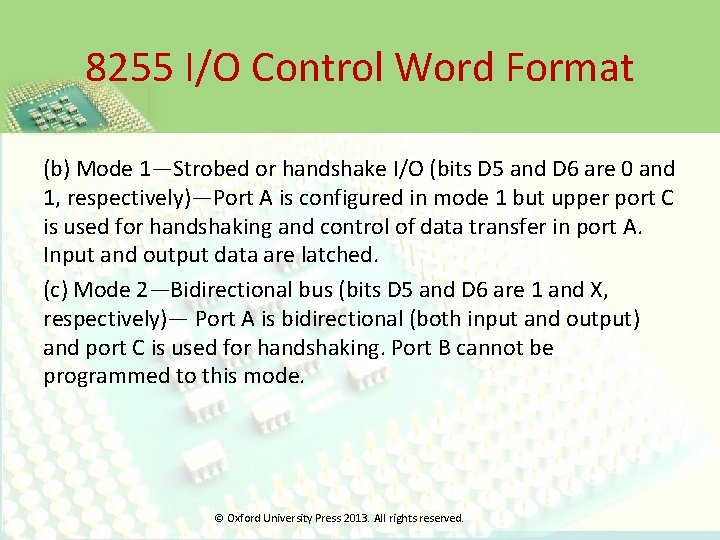
8255 I/O Control Word Format (b) Mode 1—Strobed or handshake I/O (bits D 5 and D 6 are 0 and 1, respectively)—Port A is configured in mode 1 but upper port C is used for handshaking and control of data transfer in port A. Input and output data are latched. (c) Mode 2—Bidirectional bus (bits D 5 and D 6 are 1 and X, respectively)— Port A is bidirectional (both input and output) and port C is used for handshaking. Port B cannot be programmed to this mode. © Oxford University Press 2013. All rights reserved.

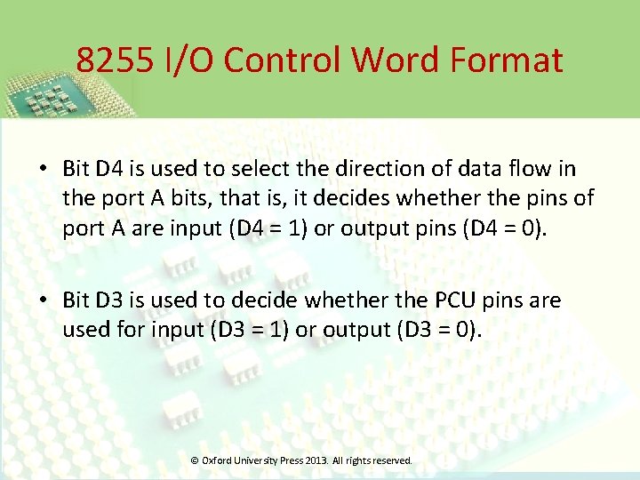
8255 I/O Control Word Format • Bit D 4 is used to select the direction of data flow in the port A bits, that is, it decides whether the pins of port A are input (D 4 = 1) or output pins (D 4 = 0). • Bit D 3 is used to decide whether the PCU pins are used for input (D 3 = 1) or output (D 3 = 0). © Oxford University Press 2013. All rights reserved.

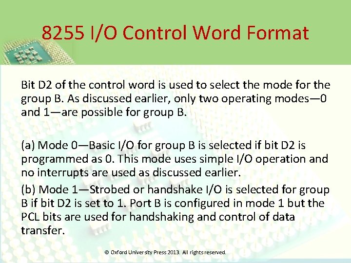
8255 I/O Control Word Format Bit D 2 of the control word is used to select the mode for the group B. As discussed earlier, only two operating modes— 0 and 1—are possible for group B. (a) Mode 0—Basic I/O for group B is selected if bit D 2 is programmed as 0. This mode uses simple I/O operation and no interrupts are used as discussed earlier. (b) Mode 1—Strobed or handshake I/O is selected for group B if bit D 2 is set to 1. Port B is configured in mode 1 but the PCL bits are used for handshaking and control of data transfer. © Oxford University Press 2013. All rights reserved.

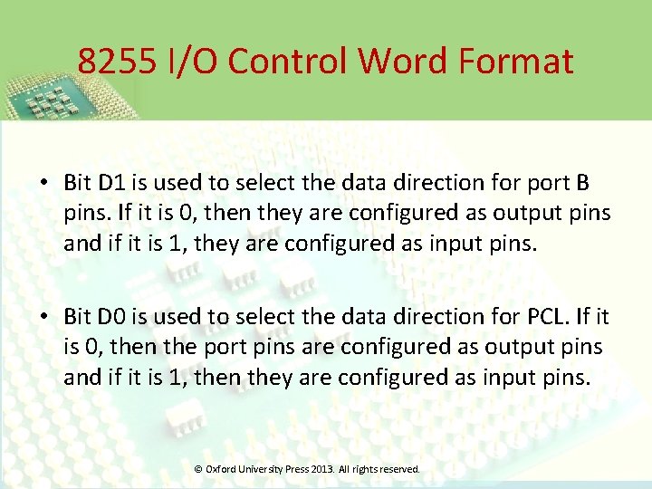
8255 I/O Control Word Format • Bit D 1 is used to select the data direction for port B pins. If it is 0, then they are configured as output pins and if it is 1, they are configured as input pins. • Bit D 0 is used to select the data direction for PCL. If it is 0, then the port pins are configured as output pins and if it is 1, then they are configured as input pins. © Oxford University Press 2013. All rights reserved.

8255 I/O Control Word Format • Bit D 1 is used to select the data direction for port B pins. If it is 0, then they are configured as output pins and if it is 1, they are configured as input pins. • Bit D 0 is used to select the data direction for PCL. If it is 0, then the port pins are configured as output pins and if it is 1, then they are configured as input pins. © Oxford University Press 2013. All rights reserved.

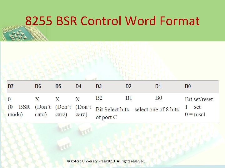
8255 BSR Control Word Format © Oxford University Press 2013. All rights reserved.

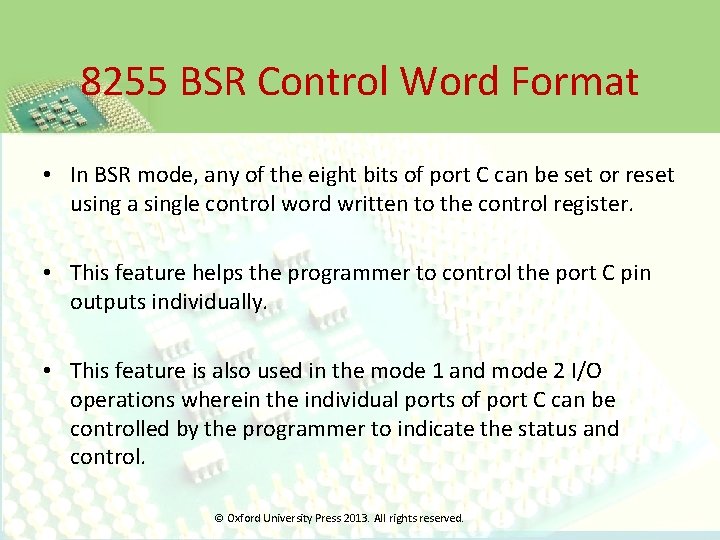
8255 BSR Control Word Format • In BSR mode, any of the eight bits of port C can be set or reset using a single control word written to the control register. • This feature helps the programmer to control the port C pin outputs individually. • This feature is also used in the mode 1 and mode 2 I/O operations wherein the individual ports of port C can be controlled by the programmer to indicate the status and control. © Oxford University Press 2013. All rights reserved.

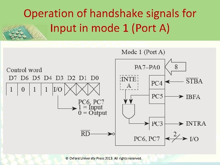
Operation of handshake signals for Input in mode 1 (Port A) © Oxford University Press 2013. All rights reserved.

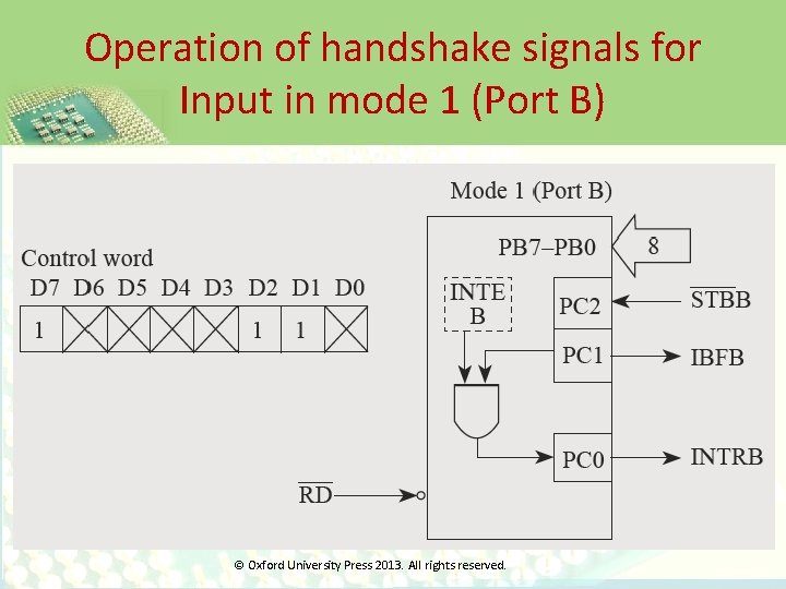
Operation of handshake signals for Input in mode 1 (Port B) © Oxford University Press 2013. All rights reserved.

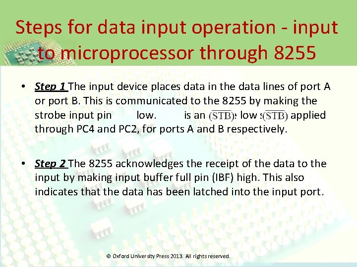
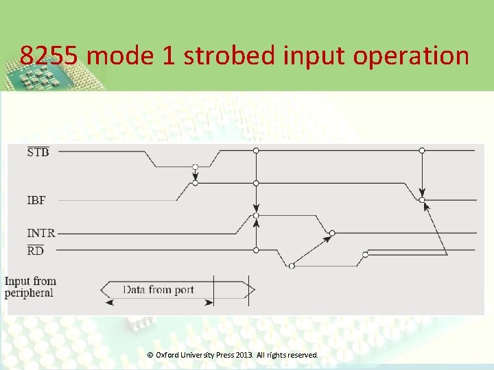
Steps for data input operation - input to microprocessor through 8255 • Step 1 The input device places data in the data lines of port A or port B. This is communicated to the 8255 by making the strobe input pin low. is an active low signal applied through PC 4 and PC 2, for ports A and B respectively. • Step 2 The 8255 acknowledges the receipt of the data to the input by making input buffer full pin (IBF) high. This also indicates that the data has been latched into the input port. © Oxford University Press 2013. All rights reserved.

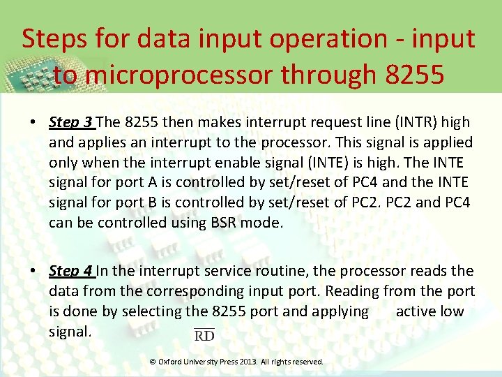
Steps for data input operation - input to microprocessor through 8255 • Step 3 The 8255 then makes interrupt request line (INTR) high and applies an interrupt to the processor. This signal is applied only when the interrupt enable signal (INTE) is high. The INTE signal for port A is controlled by set/reset of PC 4 and the INTE signal for port B is controlled by set/reset of PC 2 and PC 4 can be controlled using BSR mode. • Step 4 In the interrupt service routine, the processor reads the data from the corresponding input port. Reading from the port is done by selecting the 8255 port and applying active low signal. © Oxford University Press 2013. All rights reserved.

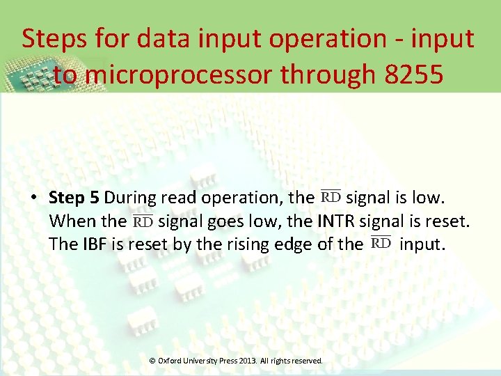
Steps for data input operation - input to microprocessor through 8255 • Step 5 During read operation, the signal is low. When the signal goes low, the INTR signal is reset. The IBF is reset by the rising edge of the input. © Oxford University Press 2013. All rights reserved.

8255 mode 1 strobed input operation © Oxford University Press 2013. All rights reserved.

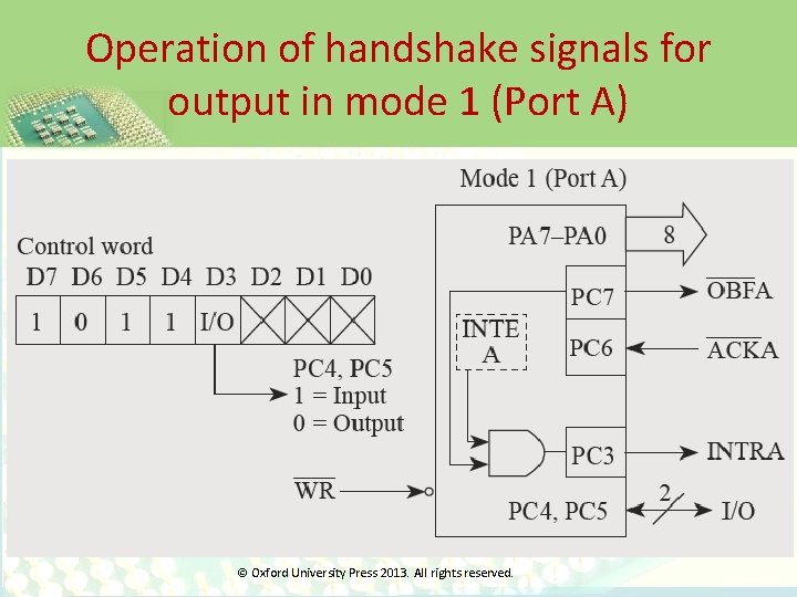
Operation of handshake signals for output in mode 1 (Port A) © Oxford University Press 2013. All rights reserved.

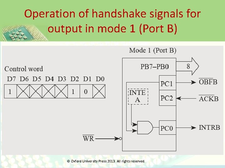
Operation of handshake signals for output in mode 1 (Port B) © Oxford University Press 2013. All rights reserved.

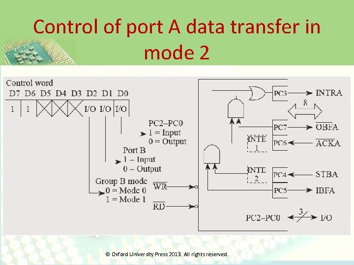
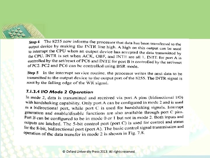
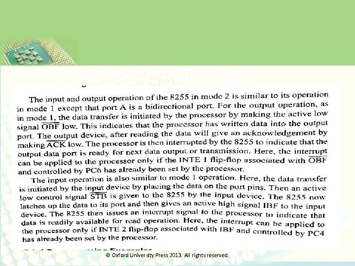
Control of port A data transfer in mode 2 © Oxford University Press 2013. All rights reserved.

© Oxford University Press 2013. All rights reserved.

© Oxford University Press 2013. All rights reserved.

© Oxford University Press 2013. All rights reserved.

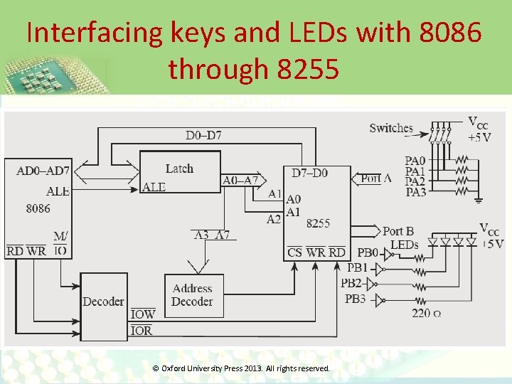
Interfacing keys and LEDs with 8086 through 8255 © Oxford University Press 2013. All rights reserved.

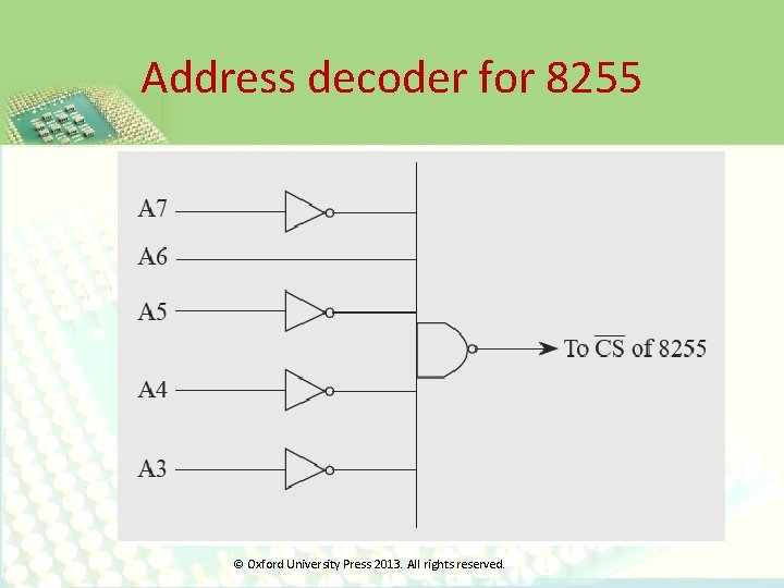
Address decoder for 8255 © Oxford University Press 2013. All rights reserved.

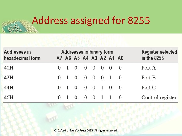
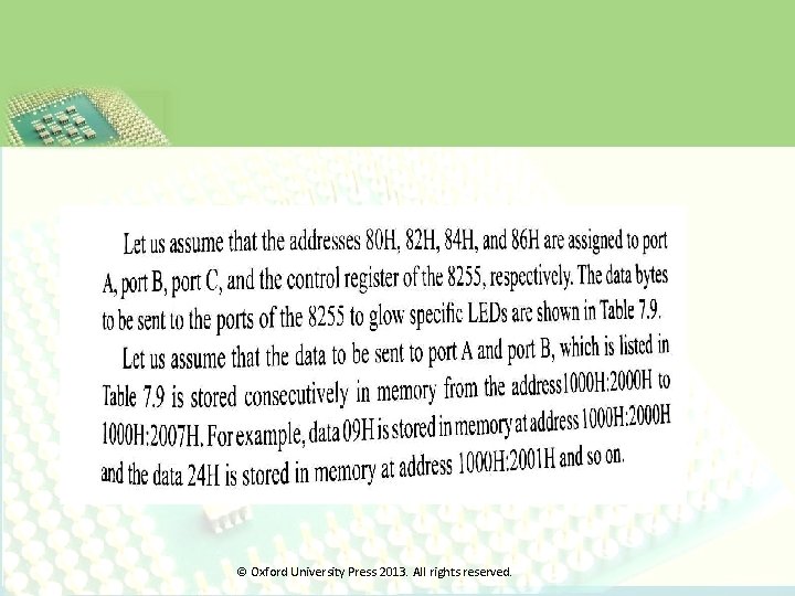
Address assigned for 8255 © Oxford University Press 2013. All rights reserved.

Bouncing of Keys • A key, in general, is a type of push-button switch, toggle switch, or electromechanical relay, having spring contacts. • Metal contacts make and break the circuit and carry the current in switches and relays. These contacts have mass and contain springs to control the movement. • Since the moving contacts have mass and springs, with low damping they will be ‘bouncy’ as they make and break. © Oxford University Press 2013. All rights reserved.

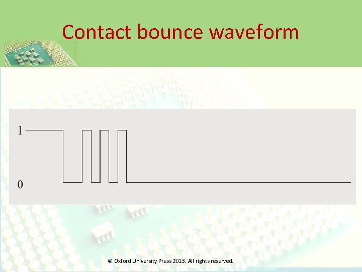
Bouncing of Keys • When a normally open (NO) pair of contacts is closed, the contacts will come together and bounce off each other several times before finally coming to rest in a closed position. • The effect is called contact bounce or, in a switch, it is called switch bounce. © Oxford University Press 2013. All rights reserved.

Contact bounce waveform © Oxford University Press 2013. All rights reserved.

Contact bounce waveform • If such a switch is used for sensing by input ports of a microprocessor, then there is a chance that the microprocessor will respond several times, i. e. , input will be sensed repeatedly even though the key is pressed only once. © Oxford University Press 2013. All rights reserved.

© Oxford University Press 2013. All rights reserved.

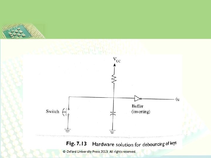
Bouncing - hardware solution • Resistor capacitor (RC) time constant to suppress the bounce and the circuit. • The RC time constant has to be larger than the switch bounce and is generally around 0. 1 s. • The capacitor takes at least twice the time constant to change from one position to the other. • During this time, any change in the switch position is not transmitted beyond the buffer. • The buffer, after the switch is used to make the transition from high-to-low or low-to-high sharp. © Oxford University Press 2013. All rights reserved.

Bouncing - software solution • Make the processor wait until the bouncing oscillation settles down. • This wait-and-see technique is implemented using software time delays. • When the voltage from the switch changes, an appropriate delay routine is executed and the value of the voltage on the switch line is checked again to make sure that the line has stopped bouncing. • The delay is normally 10 ms as in most of the switches, the oscillations settle within that period. © Oxford University Press 2013. All rights reserved.

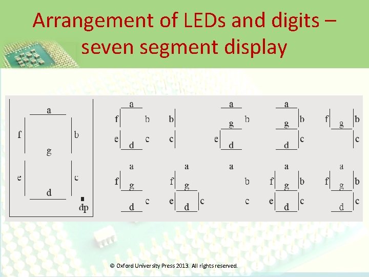
Arrangement of LEDs and digits – seven segment display © Oxford University Press 2013. All rights reserved.

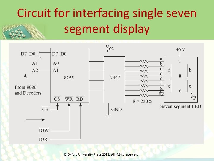
Circuit for interfacing single seven segment display © Oxford University Press 2013. All rights reserved.

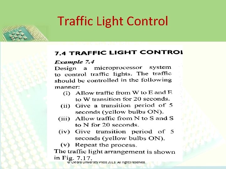
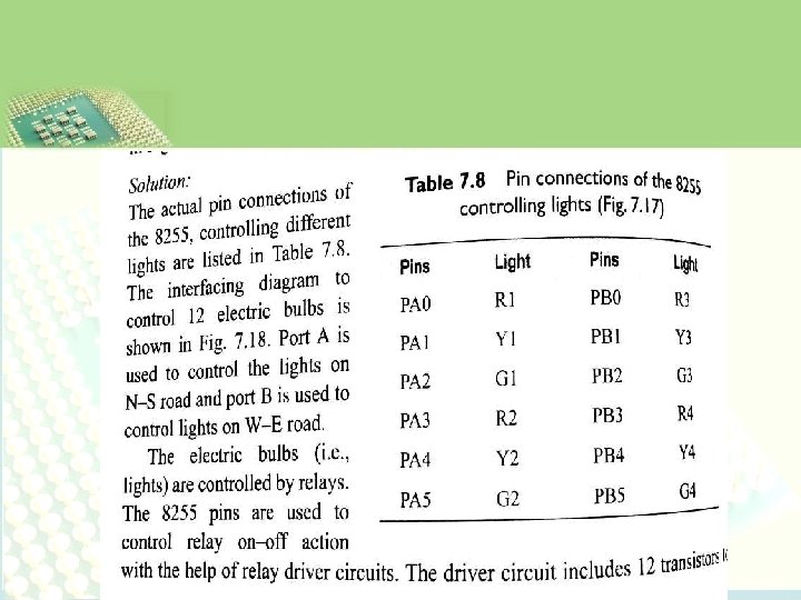
Traffic Light Control © Oxford University Press 2013. All rights reserved.

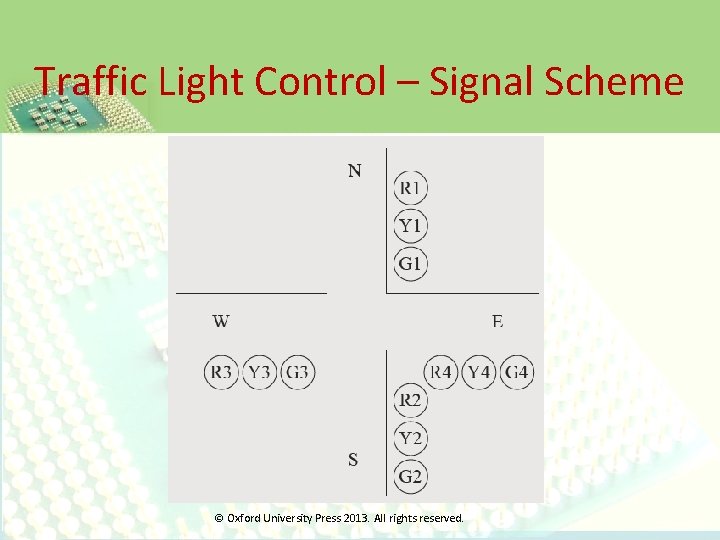
Traffic Light Control – Signal Scheme © Oxford University Press 2013. All rights reserved.

© Oxford University Press 2013. All rights reserved.

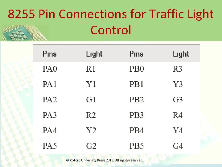
8255 Pin Connections for Traffic Light Control © Oxford University Press 2013. All rights reserved.

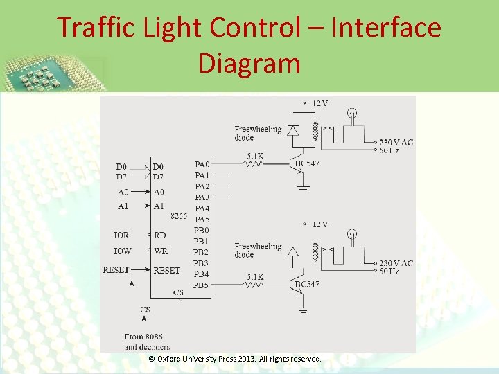
Traffic Light Control – Interface Diagram © Oxford University Press 2013. All rights reserved.

© Oxford University Press 2013. All rights reserved.

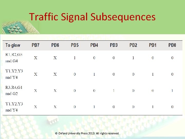
Traffic Signal Subsequences © Oxford University Press 2013. All rights reserved.

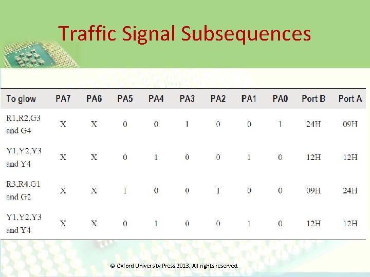
Traffic Signal Subsequences © Oxford University Press 2013. All rights reserved.

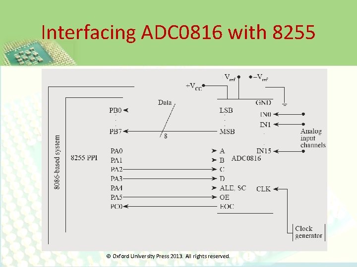
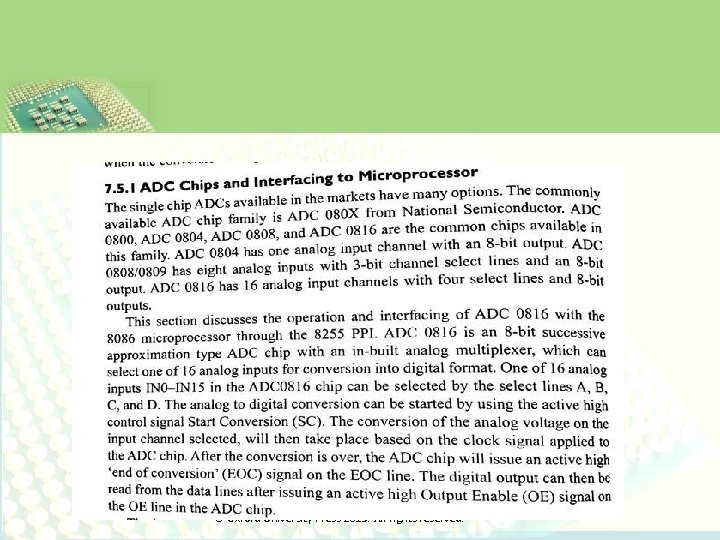
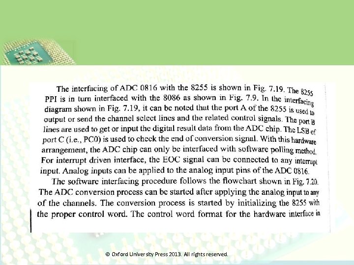
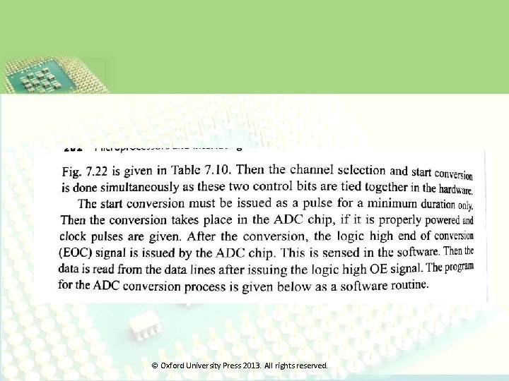
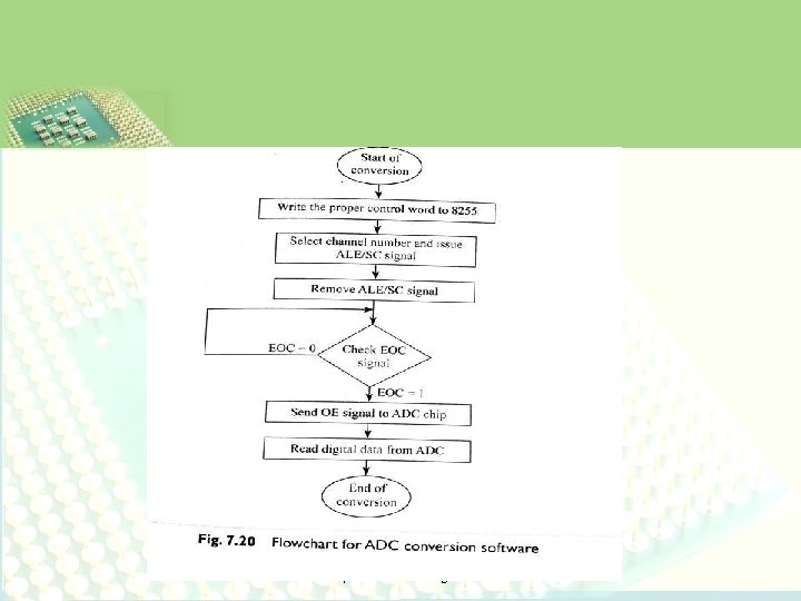
Interfacing ADC 0816 with 8255 © Oxford University Press 2013. All rights reserved.

© Oxford University Press 2013. All rights reserved.

© Oxford University Press 2013. All rights reserved.

© Oxford University Press 2013. All rights reserved.

© Oxford University Press 2013. All rights reserved.

© Oxford University Press 2013. All rights reserved.

© Oxford University Press 2013. All rights reserved.

© Oxford University Press 2013. All rights reserved.

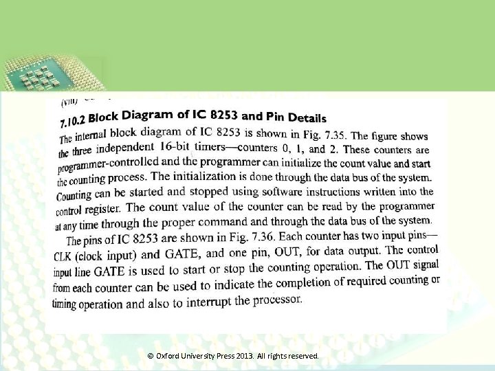
Intel Timer IC 8253 • In software programming of the 8086, it has been shown that a delay subroutine can be programmed to introduce a predefined time delay. • The delay is achieved by decrementing a count value in a register using instructions. The disadvantage of this software approach is that the processor is locked in the delay loop and precious processor time is lost in counting. • This can be overcome by using hardware timer and interrupts. © Oxford University Press 2013. All rights reserved.

Intel Timer IC 8253 • IC 555 can be used to generate the timing signals, but only at a fixed time interval. This cannot be easily interfaced with the microprocessor. • Intel finally produced programmable timer devices namely IC 8253 and IC 8254. • These ICs can be programmed to generate different types of delay signals and also count external signals. © Oxford University Press 2013. All rights reserved.

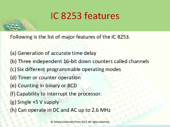
IC 8253 features Following is the list of major features of the IC 8253. (a) Generation of accurate time delay (b) Three independent 16 -bit down counters called channels (c) Six different programmable operating modes (d) Timer or counter operation (e) Counting in binary or BCD (f) Capability to interrupt the processor. (g) Single +5 V supply (h) Can operate in DC and AC up to 2. 6 MHz © Oxford University Press 2013. All rights reserved.

© Oxford University Press 2013. All rights reserved.

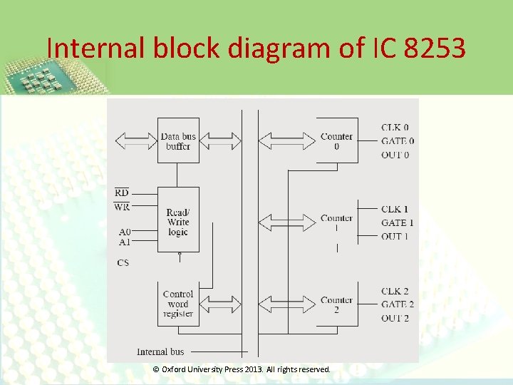
Internal block diagram of IC 8253 © Oxford University Press 2013. All rights reserved.

© Oxford University Press 2013. All rights reserved.

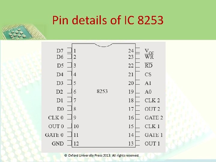
Pin details of IC 8253 © Oxford University Press 2013. All rights reserved.

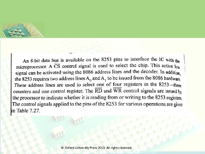
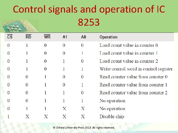
Control signals and operation of IC 8253 © Oxford University Press 2013. All rights reserved.

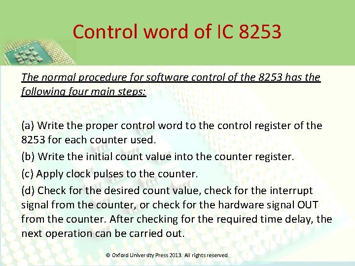
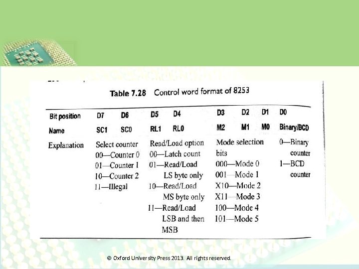
Control word of IC 8253 The normal procedure for software control of the 8253 has the following four main steps: (a) Write the proper control word to the control register of the 8253 for each counter used. (b) Write the initial count value into the counter register. (c) Apply clock pulses to the counter. (d) Check for the desired count value, check for the interrupt signal from the counter, or check for the hardware signal OUT from the counter. After checking for the required time delay, the next operation can be carried out. © Oxford University Press 2013. All rights reserved.

© Oxford University Press 2013. All rights reserved.

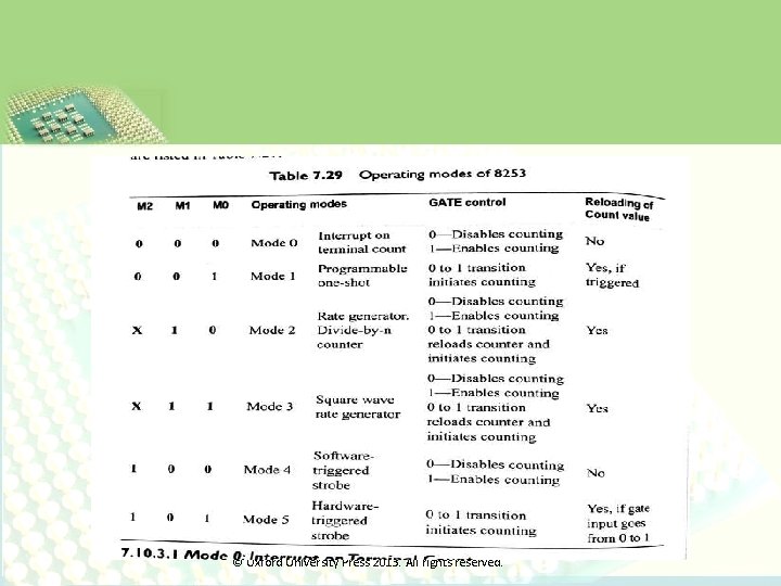
© Oxford University Press 2013. All rights reserved.

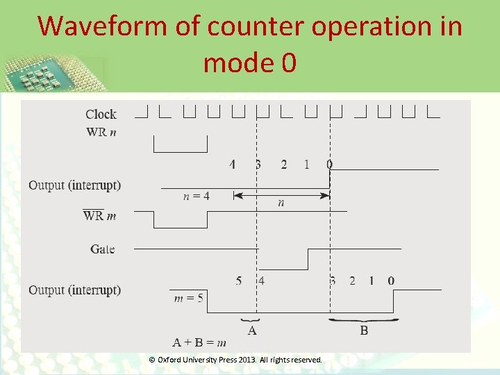
Waveform of counter operation in mode 0 © Oxford University Press 2013. All rights reserved.

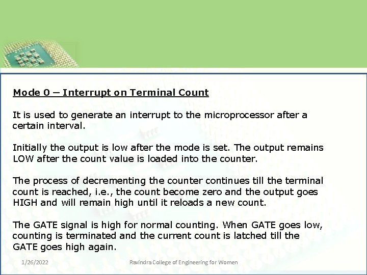
Mode 0 ─ Interrupt on Terminal Count It is used to generate an interrupt to the microprocessor after a certain interval. Initially the output is low after the mode is set. The output remains LOW after the count value is loaded into the counter. The process of decrementing the counter continues till the terminal count is reached, i. e. , the count become zero and the output goes HIGH and will remain high until it reloads a new count. The GATE signal is high for normal counting. When GATE goes low, counting is terminated and the current count is latched till the GATE goes high again. 1/26/2022 Ravindra College of Engineering for Women

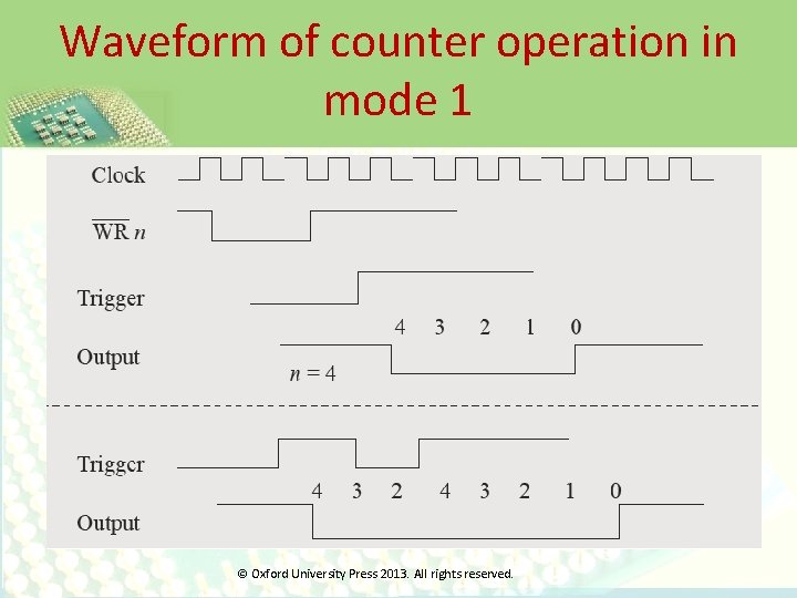
Waveform of counter operation in mode 1 © Oxford University Press 2013. All rights reserved.

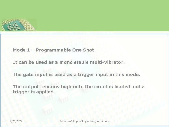
Mode 1 – Programmable One Shot It can be used as a mono stable multi-vibrator. The gate input is used as a trigger input in this mode. The output remains high until the count is loaded and a trigger is applied. 1/26/2022 Ravindra College of Engineering for Women

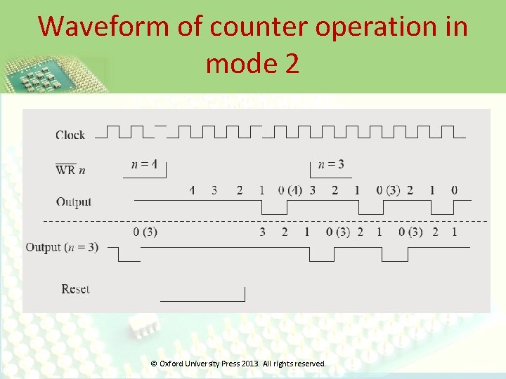
Waveform of counter operation in mode 2 © Oxford University Press 2013. All rights reserved.

Mode 2 – Rate Generator The output is normally high after initialization. Whenever the count becomes zero, another low pulse is generated at the output and the counter will be reloaded 1/26/2022 Ravindra College of Engineering for Women

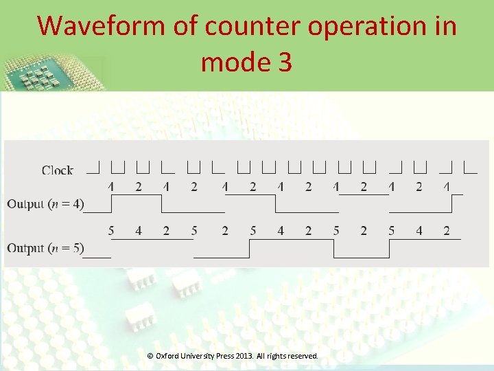
Waveform of counter operation in mode 3 © Oxford University Press 2013. All rights reserved.

Mode 3 – Square Wave Generator This mode is similar to Mode 2 except the output remains low for half of the timer period and high for the other half of the period. > If the count value is loaded with n, the output will be low for n/2 clock periods, and high for n/2 clock periods. > If n is odd the output will be high for (n+1)/2 clock periods and low for (n-1)/2 clock periods. 1/26/2022 Ravindra College of Engineering for Women

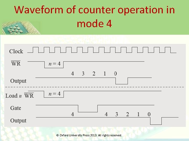
Waveform of counter operation in mode 4 © Oxford University Press 2013. All rights reserved.

Mode 4 − Software Triggered Mode In this mode, the output will remain high until the timer has counted to zero, at which point the output will pulse low and then go high again. The count is latched when the GATE signal goes LOW. On the terminal count, the output goes low for one clock cycle then goes HIGH. This low pulse can be used as a strobe. 1/26/2022 Ravindra College of Engineering for Women

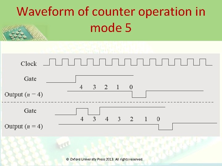
Waveform of counter operation in mode 5 © Oxford University Press 2013. All rights reserved.

Mode 5 – Hardware Triggered Mode This mode generates a strobe in response to an externally generated signal. This mode is similar to mode 4 except that the counting is initiated by a signal at the gate input, which means it is hardware triggered instead of software triggered. After it is initialized, the output goes high. When the terminal count is reached, the output goes low for one clock cycle. 1/26/2022 Ravindra College of Engineering for Women

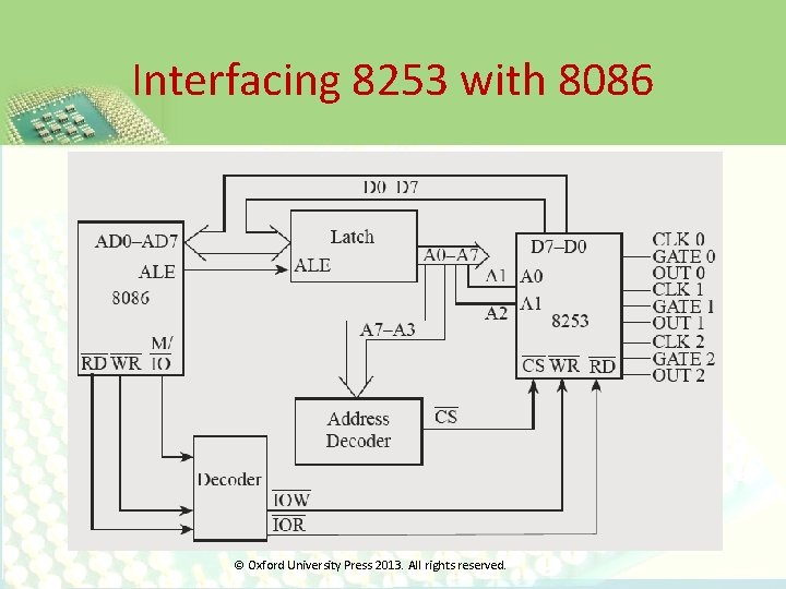
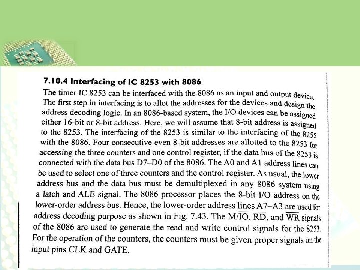
Interfacing 8253 with 8086 © Oxford University Press 2013. All rights reserved.

© Oxford University Press 2013. All rights reserved.

Serial Communication • Serial communication is sending and receiving information bit by bit. For short range communication, parallel data transfer is preferred as it is the fastest means. • While transferring data over long distances, parallel communication requires numerous wires and complex error handling/data recovery mechanisms. • For parallel data transmission of eight bits at a time, both the receiver and the transmitter side equipments need eight differential amplifiers and related hardware. © Oxford University Press 2013. All rights reserved.

Serial Communication • This results in complex circuitry and becomes costlier for long distance transmission. • Thus, serial communication is preferred for long range communication and it can be easily implemented using a single wire or a pair of wires. © Oxford University Press 2013. All rights reserved.

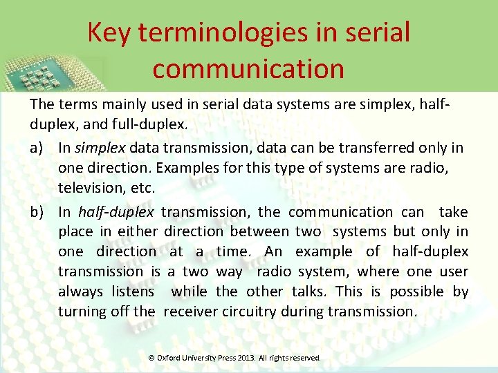
Key terminologies in serial communication The terms mainly used in serial data systems are simplex, halfduplex, and full-duplex. a) In simplex data transmission, data can be transferred only in one direction. Examples for this type of systems are radio, television, etc. b) In half-duplex transmission, the communication can take place in either direction between two systems but only in one direction at a time. An example of half-duplex transmission is a two way radio system, where one user always listens while the other talks. This is possible by turning off the receiver circuitry during transmission. © Oxford University Press 2013. All rights reserved.

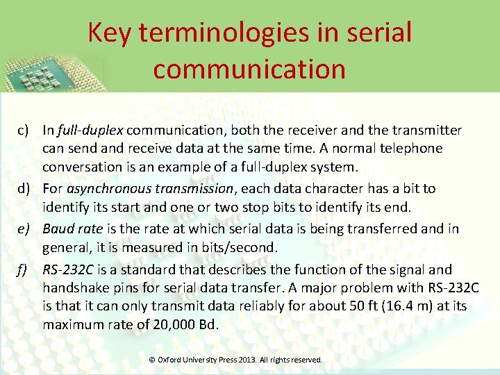
Key terminologies in serial communication c) In full-duplex communication, both the receiver and the transmitter can send and receive data at the same time. A normal telephone conversation is an example of a full-duplex system. d) For asynchronous transmission, each data character has a bit to identify its start and one or two stop bits to identify its end. e) Baud rate is the rate at which serial data is being transferred and in general, it is measured in bits/second. f) RS-232 C is a standard that describes the function of the signal and handshake pins for serial data transfer. A major problem with RS-232 C is that it can only transmit data reliably for about 50 ft (16. 4 m) at its maximum rate of 20, 000 Bd. © Oxford University Press 2013. All rights reserved.

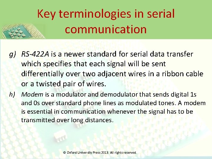
Key terminologies in serial communication g) RS-422 A is a newer standard for serial data transfer which specifies that each signal will be sent differentially over two adjacent wires in a ribbon cable or a twisted pair of wires. h) Modem is a modulator and demodulator that sends digital 1 s and 0 s over standard phone lines as modulated tones. A modem is essential in communication whenever the signal has to be transmitted over long distances. © Oxford University Press 2013. All rights reserved.

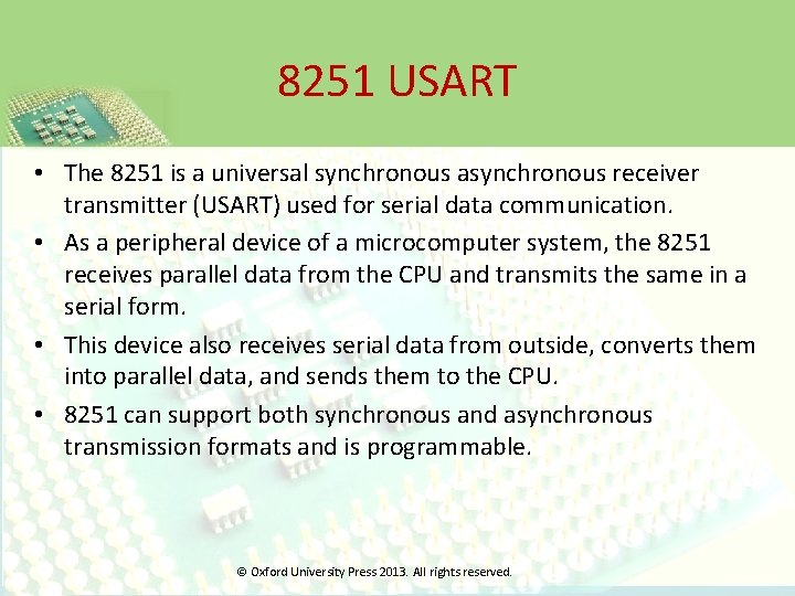
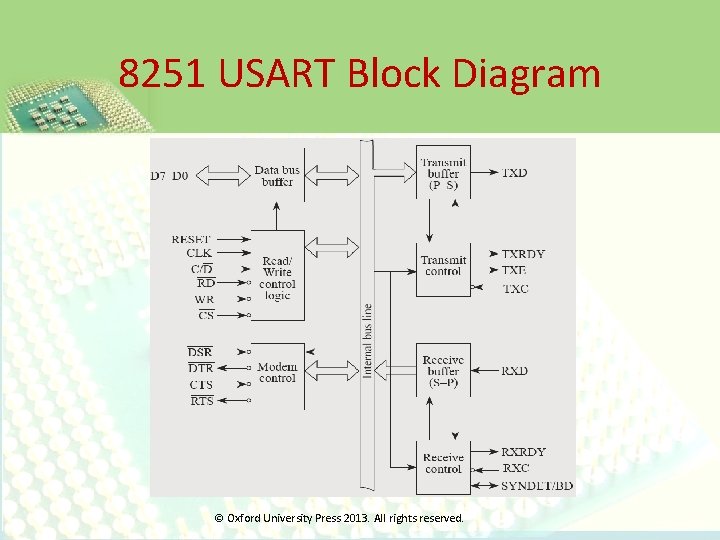
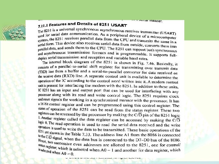
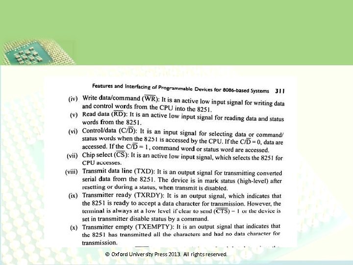
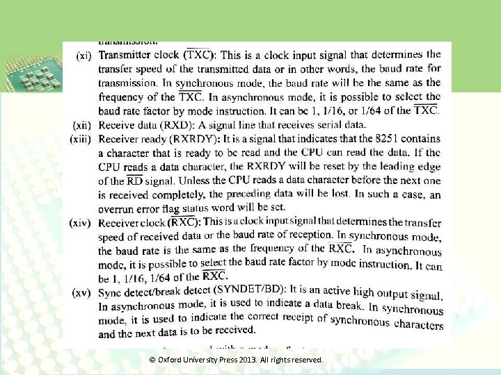
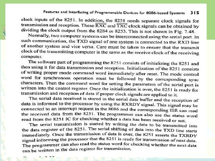
8251 USART • The 8251 is a universal synchronous asynchronous receiver transmitter (USART) used for serial data communication. • As a peripheral device of a microcomputer system, the 8251 receives parallel data from the CPU and transmits the same in a serial form. • This device also receives serial data from outside, converts them into parallel data, and sends them to the CPU. • 8251 can support both synchronous and asynchronous transmission formats and is programmable. © Oxford University Press 2013. All rights reserved.

8251 USART Block Diagram © Oxford University Press 2013. All rights reserved.

© Oxford University Press 2013. All rights reserved.

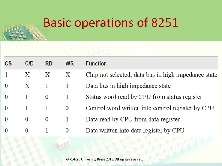
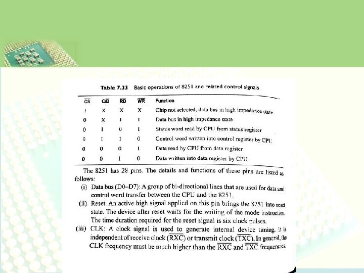
Basic operations of 8251 © Oxford University Press 2013. All rights reserved.

© Oxford University Press 2013. All rights reserved.

© Oxford University Press 2013. All rights reserved.

© Oxford University Press 2013. All rights reserved.

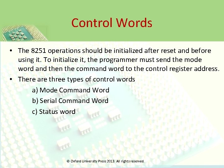
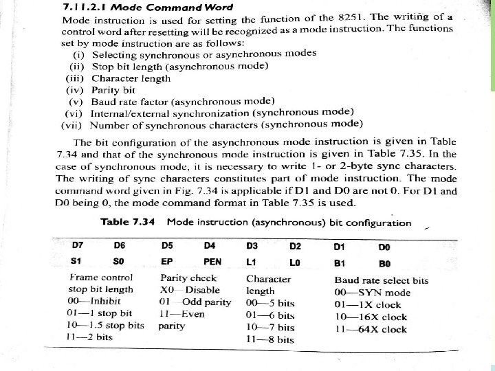
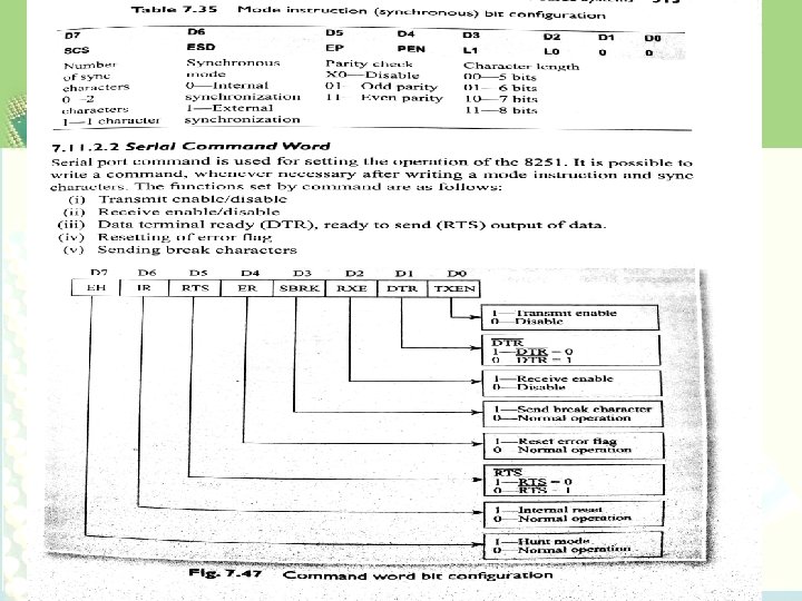
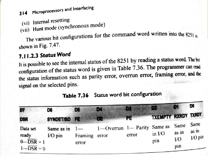
Control Words • The 8251 operations should be initialized after reset and before using it. To initialize it, the programmer must send the mode word and then the command word to the control register address. • There are three types of control words a) Mode Command Word b) Serial Command Word c) Status word © Oxford University Press 2013. All rights reserved.

© Oxford University Press 2013. All rights reserved.

© Oxford University Press 2013. All rights reserved.

© Oxford University Press 2013. All rights reserved.

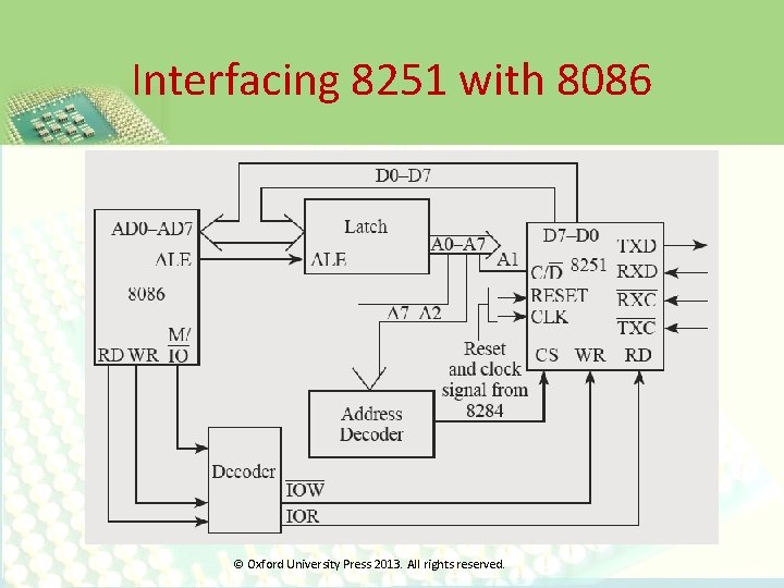
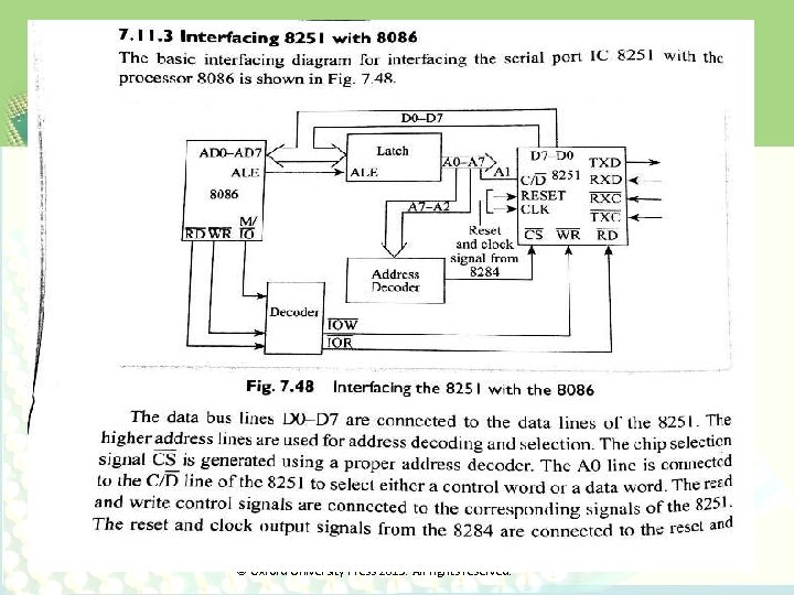
Interfacing 8251 with 8086 © Oxford University Press 2013. All rights reserved.

© Oxford University Press 2013. All rights reserved.

© Oxford University Press 2013. All rights reserved.

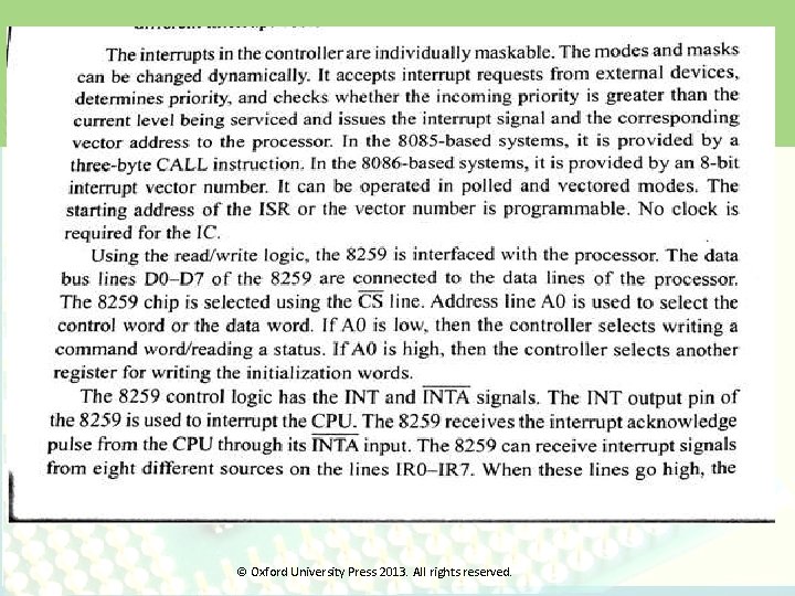
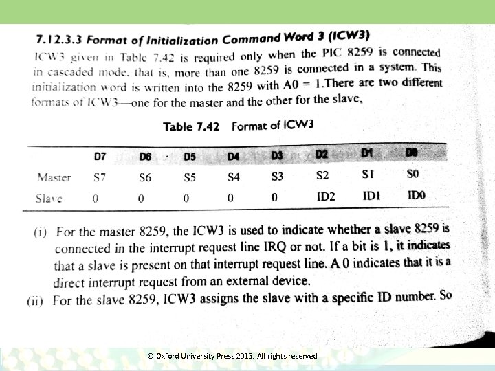
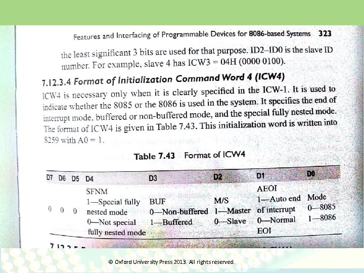
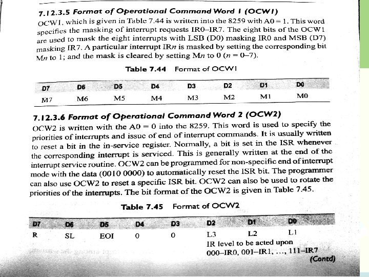
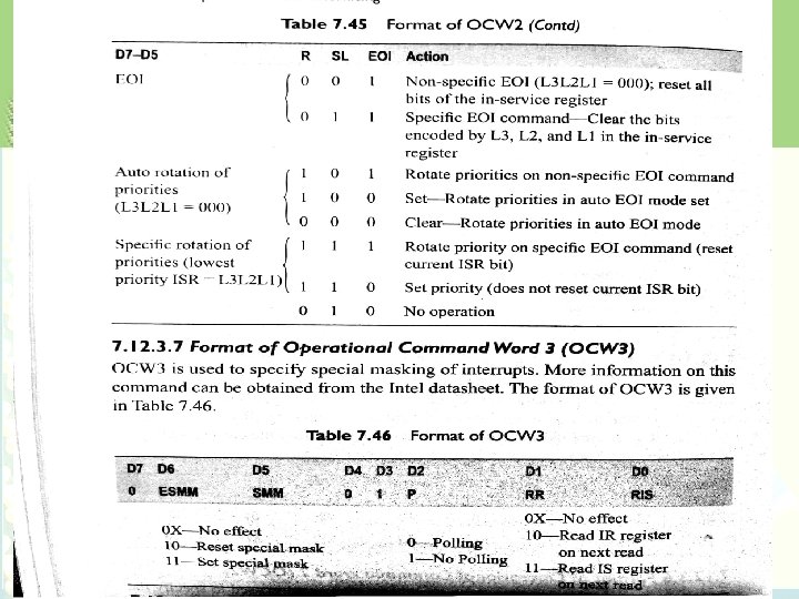
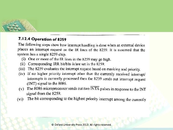
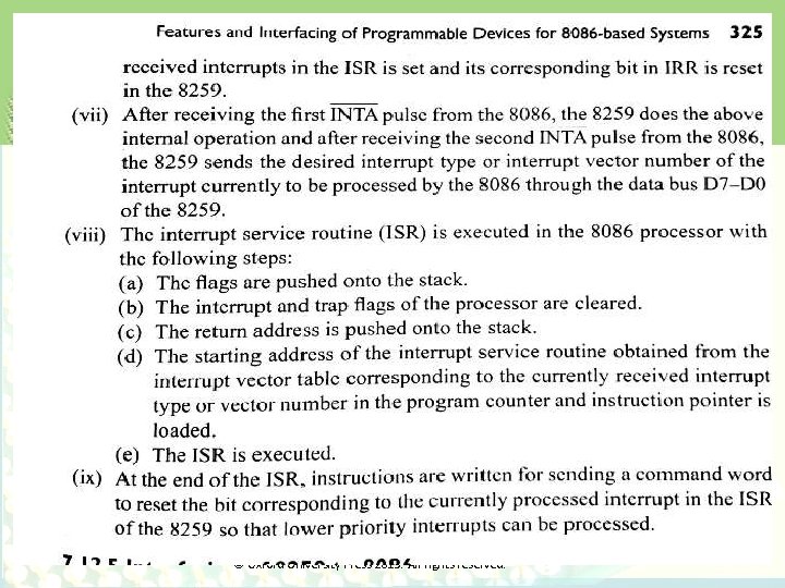
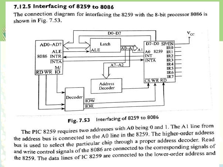
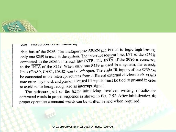
8259 Programmable Interrupt Controller • Interrupts are used in a system to handle routines such as reading ASCII characters from a keyboard, detecting and performing an emergency operations such as sounding a fire alarm. • For this, the processor’s maskable or non-maskable interrupts are used. However, the processor has limited number of hardware interrupts. • For applications that use interrupts from multiple sources, the processor can use external device called programmable interrupt controller (PIC) or priority interrupt controller. © Oxford University Press 2013. All rights reserved.

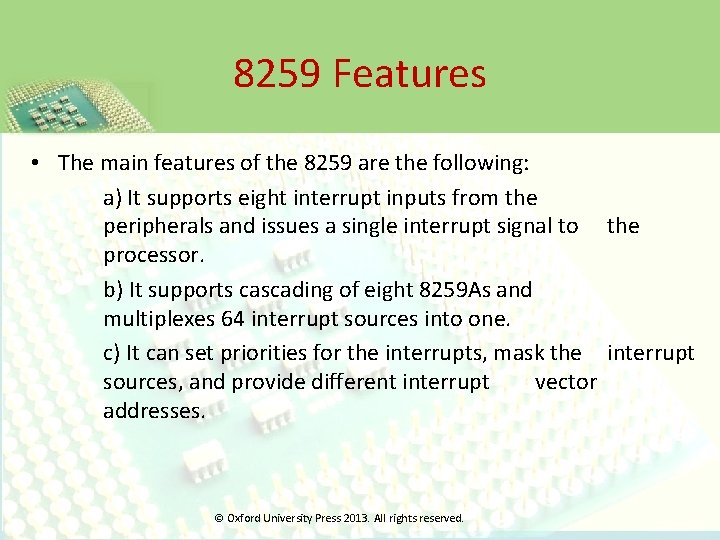
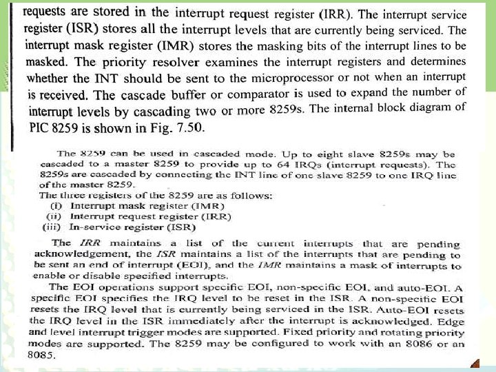
8259 Features • The main features of the 8259 are the following: a) It supports eight interrupt inputs from the peripherals and issues a single interrupt signal to the processor. b) It supports cascading of eight 8259 As and multiplexes 64 interrupt sources into one. c) It can set priorities for the interrupts, mask the interrupt sources, and provide different interrupt vector addresses. © Oxford University Press 2013. All rights reserved.

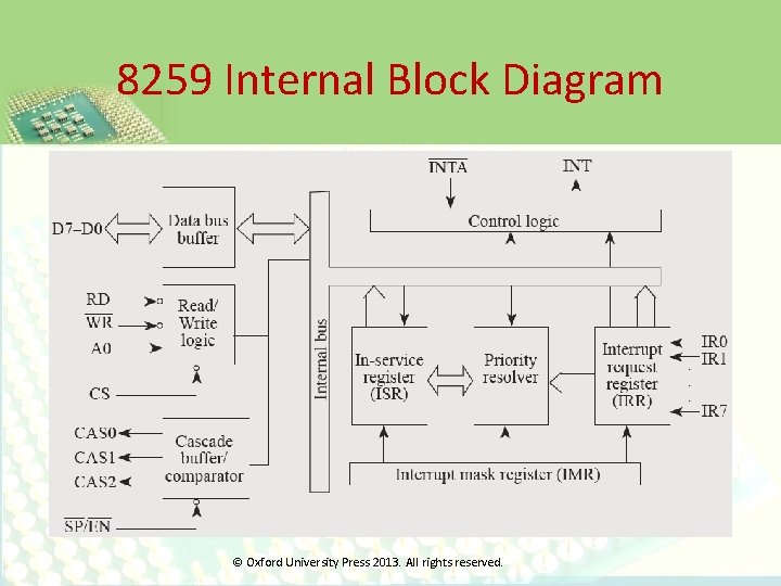
8259 Internal Block Diagram © Oxford University Press 2013. All rights reserved.

© Oxford University Press 2013. All rights reserved.

© Oxford University Press 2013. All rights reserved.

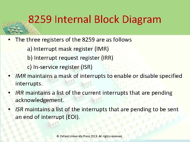
8259 Internal Block Diagram • The three registers of the 8259 are as follows a) Interrupt mask register (IMR) b) Interrupt request register (IRR) c) In-service register (ISR) • IMR maintains a mask of interrupts to enable or disable specified interrupts. • IRR maintains a list of the current interrupts that are pending acknowledgement. • ISR maintains a list of the interrupts that are pending to be sent an end of interrupt (EOI). © Oxford University Press 2013. All rights reserved.

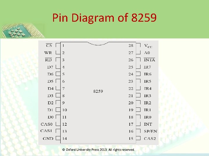
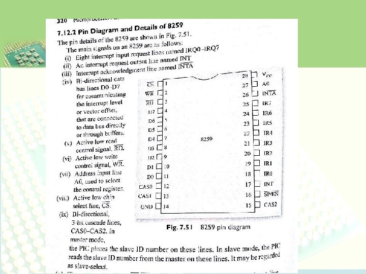
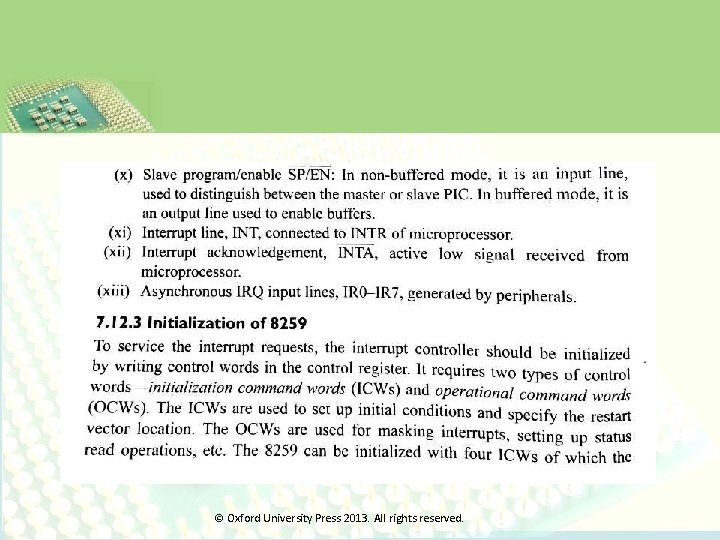
Pin Diagram of 8259 © Oxford University Press 2013. All rights reserved.

© Oxford University Press 2013. All rights reserved.

© Oxford University Press 2013. All rights reserved.

© Oxford University Press 2013. All rights reserved.

© Oxford University Press 2013. All rights reserved.

© Oxford University Press 2013. All rights reserved.

© Oxford University Press 2013. All rights reserved.

© Oxford University Press 2013. All rights reserved.

© Oxford University Press 2013. All rights reserved.

© Oxford University Press 2013. All rights reserved.

© Oxford University Press 2013. All rights reserved.

© Oxford University Press 2013. All rights reserved.

© Oxford University Press 2013. All rights reserved.

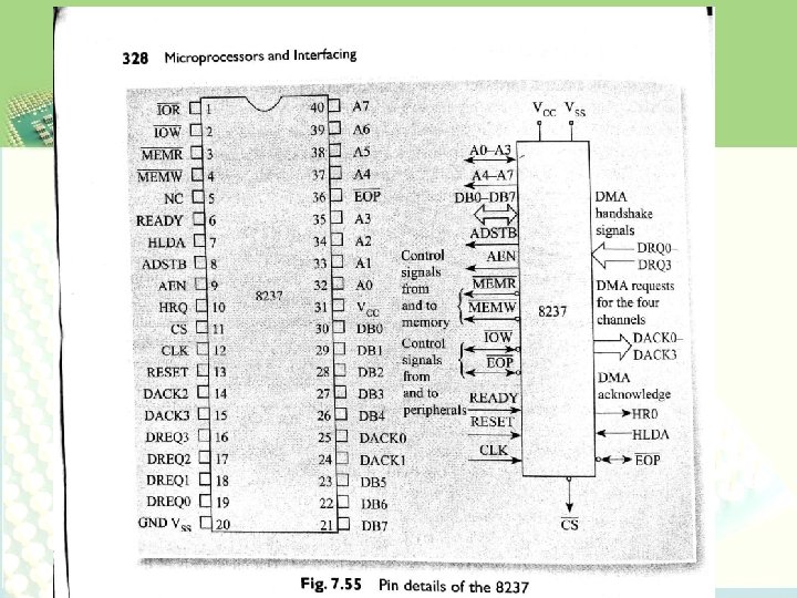
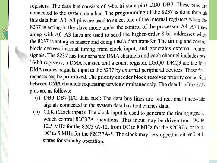
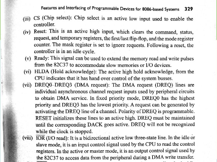
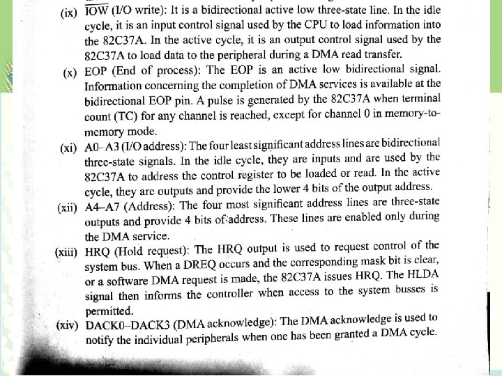
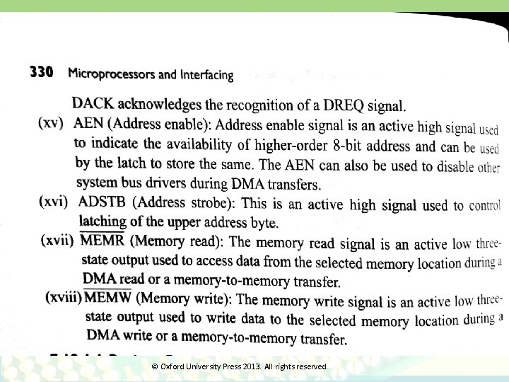
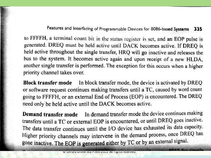
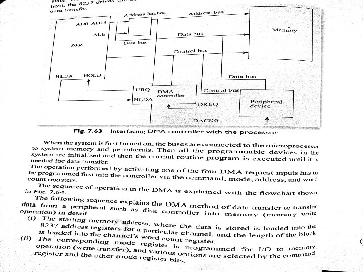
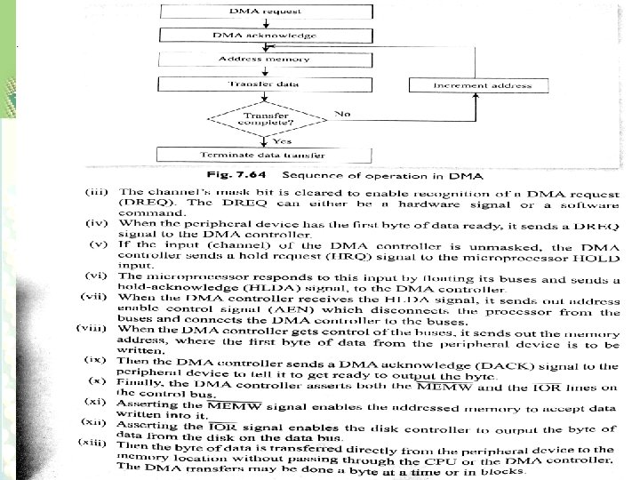
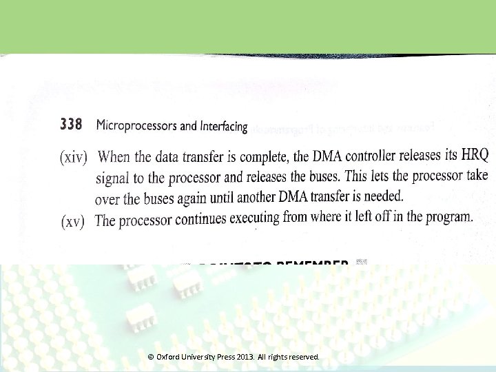
8237 DMA Controller • DMA stands for direct memory access. It is one of the ways to accomplish high-speed data transfers, directly between memory and peripheral devices. • The DMA is a method of data transfer between memory and I/O devices without the intervention of microprocessor. • This method is often used when large block of data is to be transferred. • DMA data transfer is controlled by using a separate DMA controller. © Oxford University Press 2013. All rights reserved.

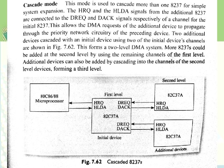
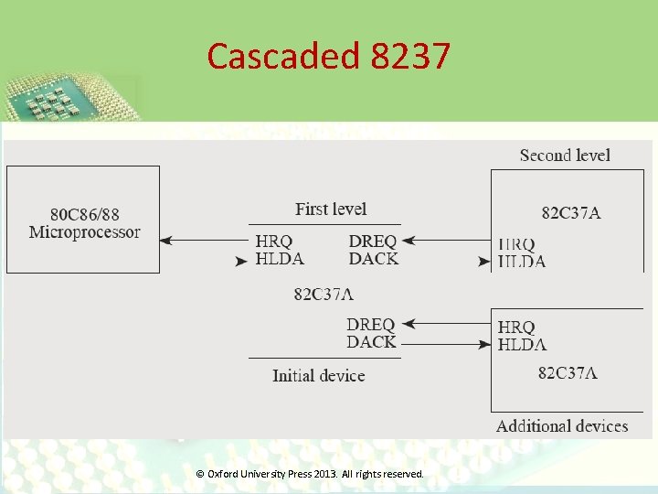
8237 DMA Controller Features • The main features of the 8237 are a) Four independent DMA channels. b) Enable and disable control of individual requests. c) Possibility for memory-to-memory transfer. d) Address increment or decrement. e) Cascading and expandable to any number of DMA channels. © Oxford University Press 2013. All rights reserved.

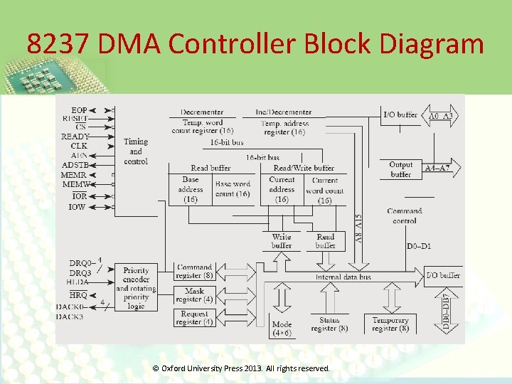
8237 DMA Controller Block Diagram © Oxford University Press 2013. All rights reserved.

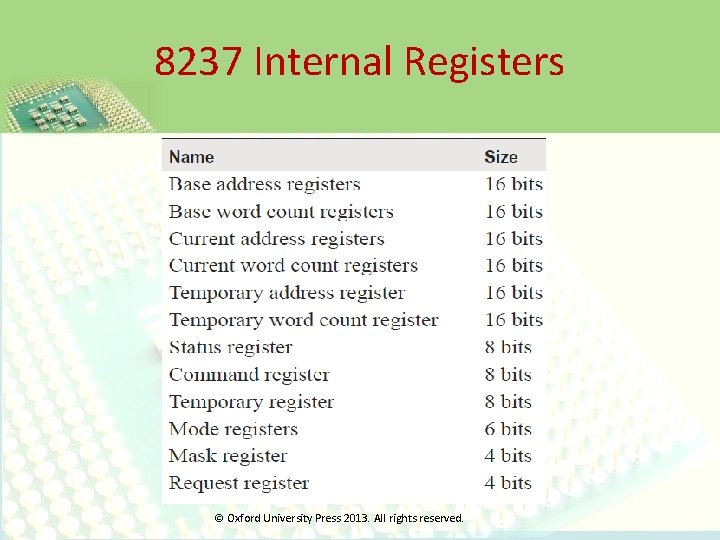
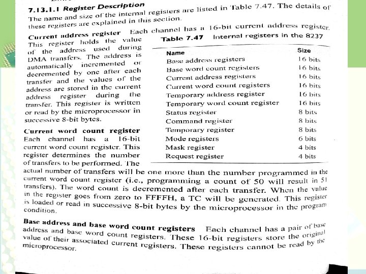
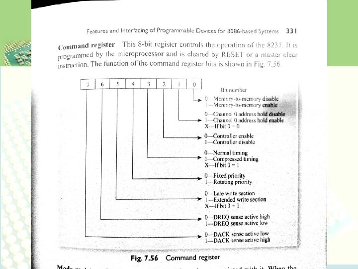
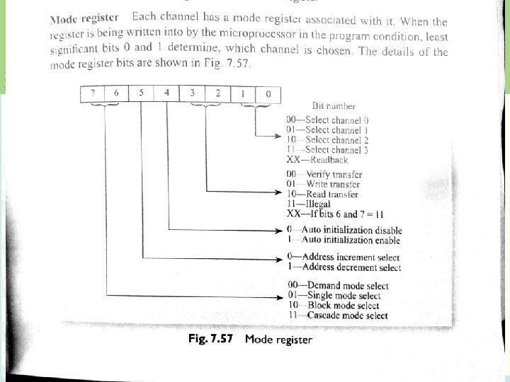
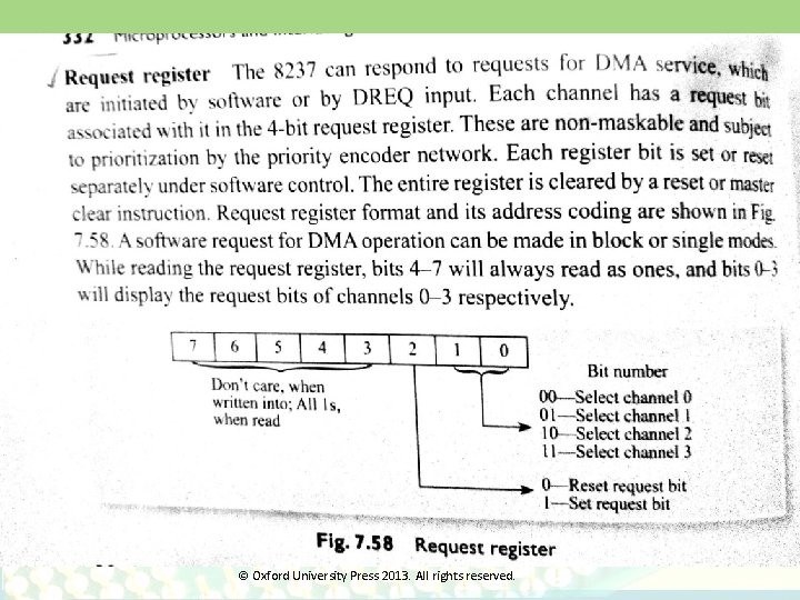
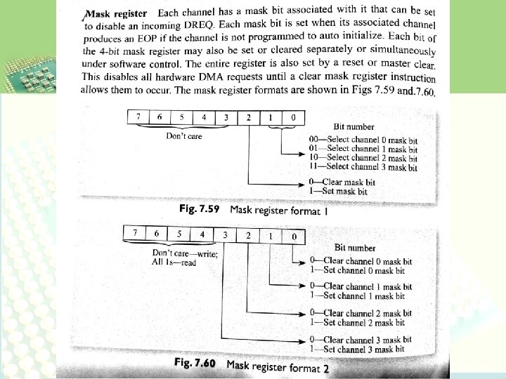
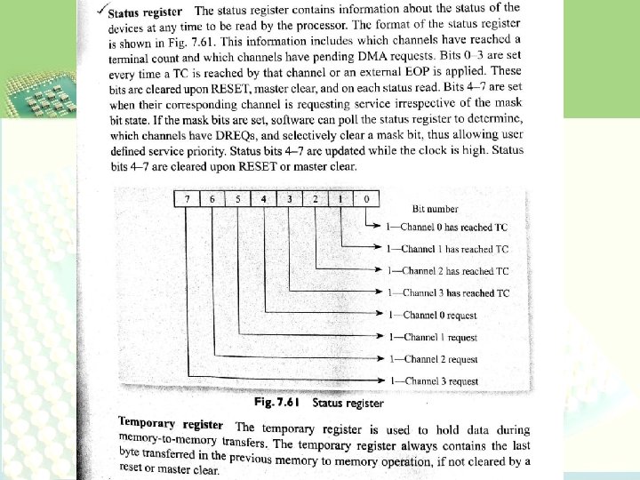
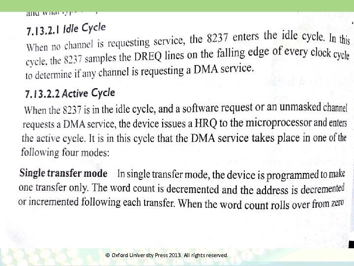
8237 Internal Registers © Oxford University Press 2013. All rights reserved.

© Oxford University Press 2013. All rights reserved.

© Oxford University Press 2013. All rights reserved.

© Oxford University Press 2013. All rights reserved.

© Oxford University Press 2013. All rights reserved.

© Oxford University Press 2013. All rights reserved.

© Oxford University Press 2013. All rights reserved.

© Oxford University Press 2013. All rights reserved.

© Oxford University Press 2013. All rights reserved.

© Oxford University Press 2013. All rights reserved.

© Oxford University Press 2013. All rights reserved.

© Oxford University Press 2013. All rights reserved.

© Oxford University Press 2013. All rights reserved.

© Oxford University Press 2013. All rights reserved.

© Oxford University Press 2013. All rights reserved.

© Oxford University Press 2013. All rights reserved.

© Oxford University Press 2013. All rights reserved.

© Oxford University Press 2013. All rights reserved.

Cascaded 8237 © Oxford University Press 2013. All rights reserved.

Summary • The Intel processor IC 8086 needs additional slave chips such as programmable peripheral interfaces, keyboard/display interfaces, serial ports, timers, interrupt controllers, and DMA controllers to interface different peripherals and to perform various functions. • Intel IC 8255 is a general purpose PPI and can be used to interface other devices such as seven-segment displays, switches, ADCs, DACs, and so on. • Multiplexed displays and matrix keyboards reduce hardware complexity and can be easily interfaced with the 8086 using the slave IC Intel 8279. © Oxford University Press 2013. All rights reserved.

Summary • The serial data transmission can be easily done by the processor with the interfacing of the IC USART 8251. • The timing of various events can be controlled by the programmer by interfacing the timer IC such as 8253 to the processor and connecting a clock to it. • There is a need of programmable interrupt controller if the number of peripherals interfaced using the interrupt driven I/O method is higher than the interrupt capability of the processor. Intel provides the programmable interrupt controller IC 8259 for such applications. © Oxford University Press 2013. All rights reserved.

Summary • The high speed data transfer between I/O devices and the processor can be achieved by using a technique called direct memory access. The DMA controller IC 8237 can be interfaced with the processor to achieve the process of direct memory access of memory by I/O devices. © Oxford University Press 2013. All rights reserved.