VLSI DESIGN TEXT BOOKS 1 Kamran Eshraghian Eshraghian

VLSI DESIGN TEXT BOOKS: 1. Kamran Eshraghian, Eshraghian Douglas and A. Pucknell, “Essentials of VLSI circuits and systems”, PHI, 2013 Edition. 2. K. Lal Kishore and V. S. V. Prabhakar, “VLSI Design”, IK Publishers REFERENCES: 1. Weste and Eshraghian, “Principles of CMOS VLSI Design”, Pearson Education, 1999. 2. Wayne Wolf, “Modern VLSI Design”, Pearson Education, 3 rd Edition, 1997. 3. John P. Uyemura, “Chip Design for Submicron VLSI: CMOS layout and Simulation”, Thomson. Learning. 4. John P. Uyemura, “Introduction to VLSI Circuits and Systems”, John wiley, 2003. 5. John M. Rabaey, “Digital Integrated Circuits”, PHI, EEE, 1997.

UNIT-I Introduction: Basic steps of IC fabrication Technologies : PMOS, NMOS, CMOS & Bi. CMOS, SOI process MOS transistors - MOS transistor switches Basic gate using switches , Working transistor as Resistors and Capacitors. Basic Electrical Properties of MOS and Bi. CMOS Circuits: Working of MOS transistors –threshold voltage; MOS design equations: Ids–Vds relationships, Threshold Voltage, Body effect, Channel length modulation , gm, gds, figure of merit ω0; Pass transistor, NMOS Inverter, CMOS Inverter analysis and design, Various pull ups loads, Bi-CMOS Inverters.

What is an IC ? Many transistors on one chip/die.

Why the Integrated circuit ? • Integration improves • size • speed • power • Integration reduce manufacturing costs

History The integrated circuit or IC was put forth by Jack Kilby at Texas Instruments
(10 -100) contained 1 – 10")
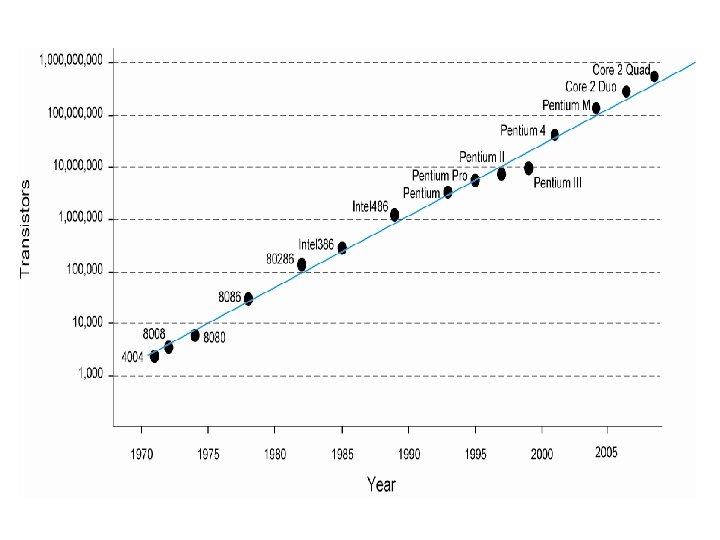
EVALUATION of IC’S SSI – Small Scale Integration( 1960)(10 -100) contained 1 – 10 ------- logic gates MSI – Medium Scale Integration (1970 )(100 -1000) logic functions, counters LSI – Large Scale Integration ( 1980 )(1000 -10000) first microprocessors on the chip VLSI – Very Large Scale Integration >10000 64 -bit microprocessors, complete with cache memory (L 1 and often L 2), floating-point arithmetic unit(s), etc

Moore's law In the year 1965 Gordon Moore Intel Co-Founder and Chairman predicted that transistors would continue to shrink , allowing : -- Doubled transistors density every 18 -24 months -- Doubled performance every 18 -24 months The period often quoted as "18 months
 P 6 Pentium ® proc 10 8086 286 1")
Power Dissipation 100 Power (Watts) P 6 Pentium ® proc 10 8086 286 1 4004 8008 8085 8080 486 386 0. 1 1974 1978 1985 1992 2000 Year Lead Microprocessors power continues to increase © Rabaey: Digital Integrated Circuits 2 nd Courtesy, Intel
 – ECL (emitter-coupled logic) •")
IC -Technologies • Bipolar technology – TTL (transistor-transistor logic) – ECL (emitter-coupled logic) • MOS (Metal-oxide-silicon) – n. MOS (n-channel MOS) – p. MOS (p-channel MOS) – CMOS • Bi CMOS technology
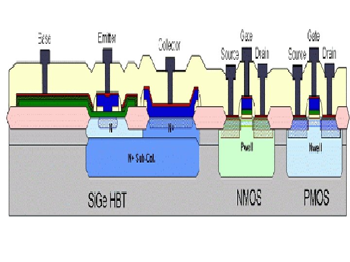
 • Si-Ge - Silicon")
• Ga. As - Gallium Arsenide (for high speed) • Si-Ge - Silicon Germanium (for RF)

IC –Manufacturing 4 - stages • Material Preparation • Crystal Growing and Wafer preparation • Wafer fabrication • Testing , Bonding and Packaging

Material Preparation

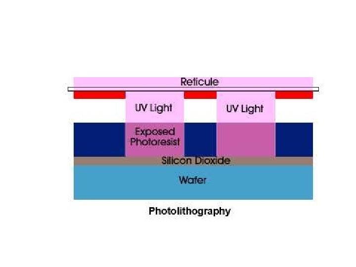
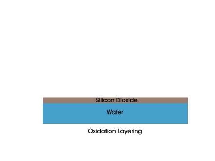
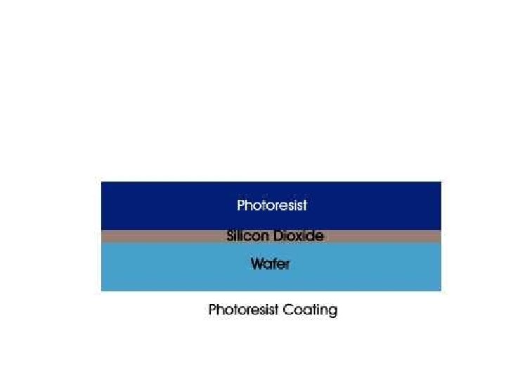
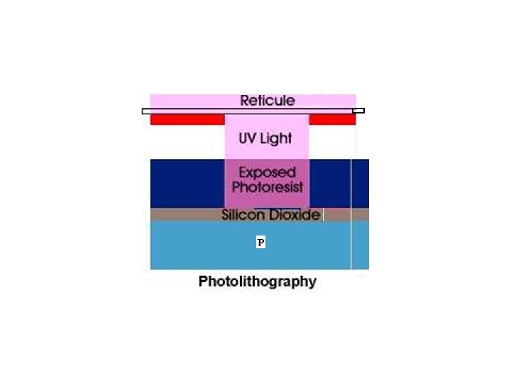
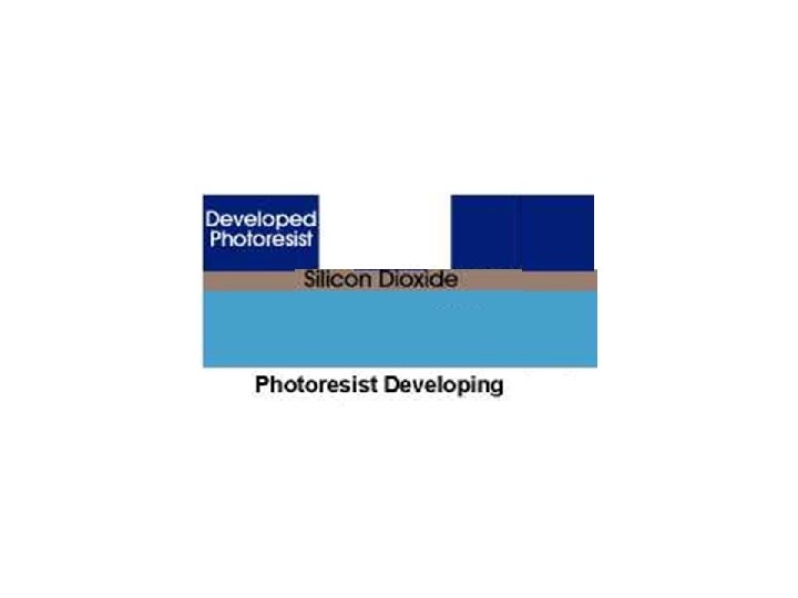
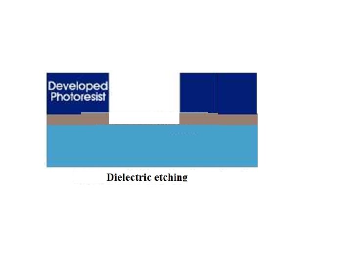
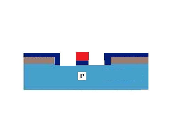
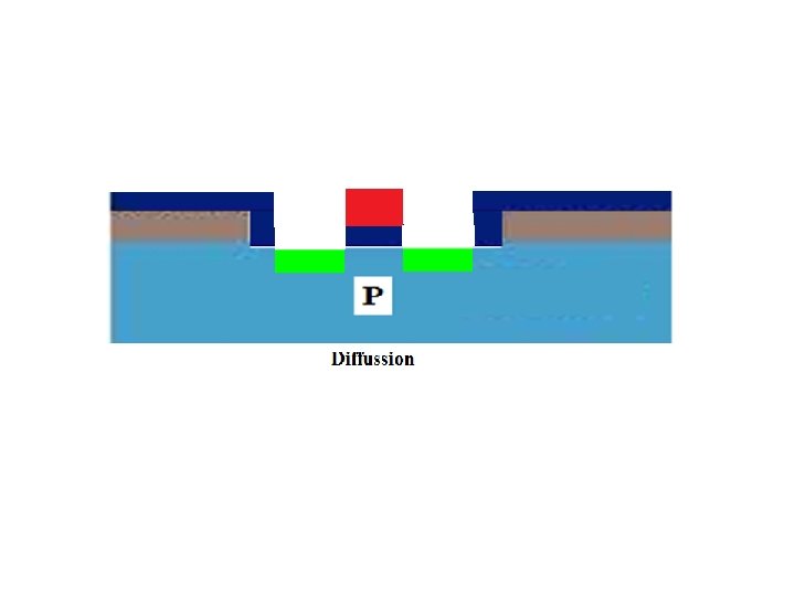
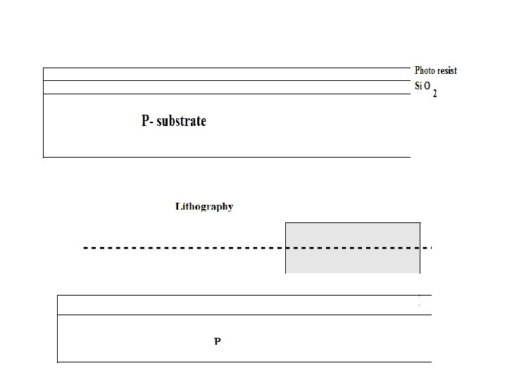
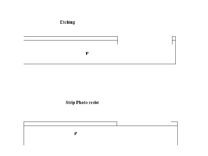
Wafer fabrication • Oxidation • Etching • Diffussion • Photolithography • Epitaxy • Metallization and interconnections

Oxidation is a process which converts silicon on the wafer into silicon dioxide

Etching is used to remove material selectively in order to create patterns

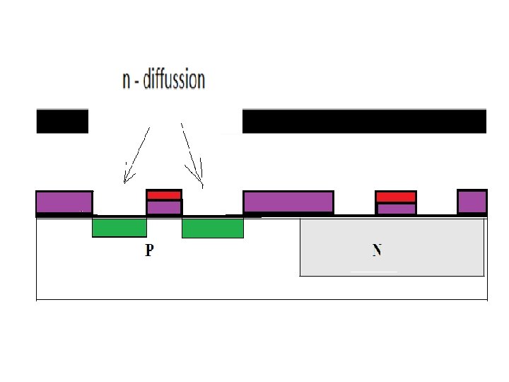
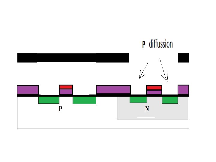
Diffussion The deposition of the desired impurity on the silicon surface through windows, and then move the impurity atoms from the surface into the silicon crystal.

Photolithography Lithography is used to transfer a pattern from a photomask to the surface of the wafer

Epitaxy The process of the controlled growth of crystalline doped layer of Si on a single crystal substrate.

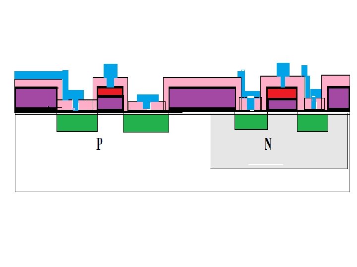
Metallization and interconnections The process of metallization is used to provide internal and external connections.

n MOS - FABRICATION
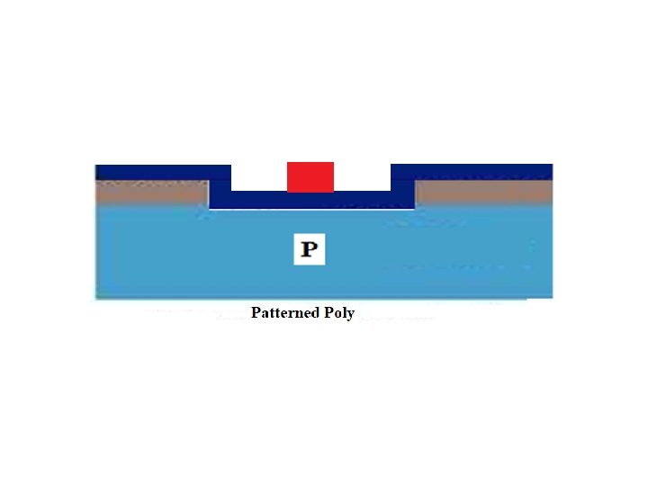
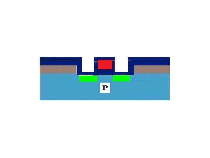
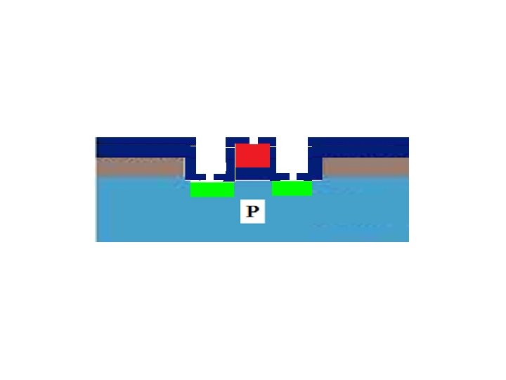
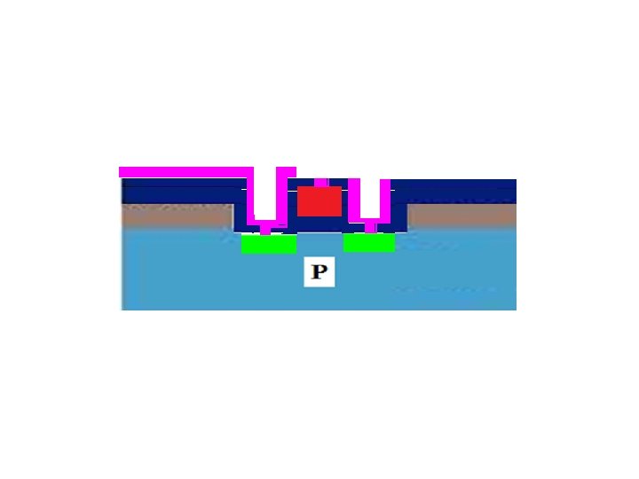
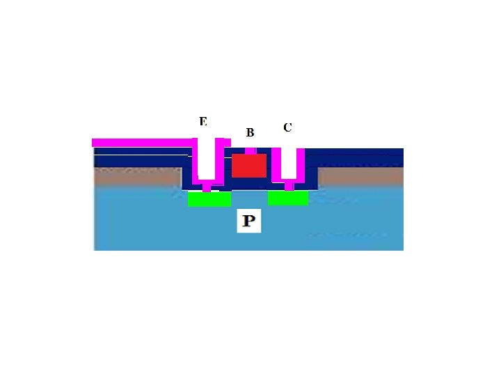

Summary of n-MOS process Mask-I – Pattern Si. O 2 – to expose Si surface where diffusing has to takes place. Mask-2 – Pattern thinox region where depletion mode devices are to be produced. Mask-3 – Pattern the Poly Si. Mask-4 – to Diffusion p type semiconductor Mask-5 – Pattern the metal Mask-6 – Would be required for the over glassing process

CMOS FABRICATION • P-Well • N-well • Twin- tub • Silicon-on-Insulator

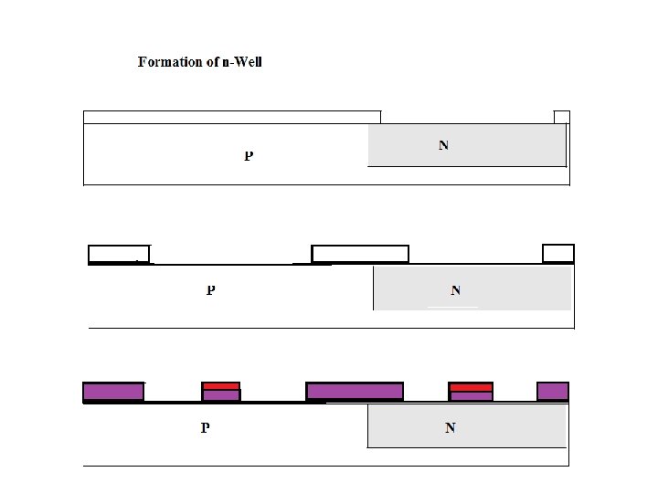
n-Well

Twin Tub

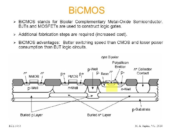
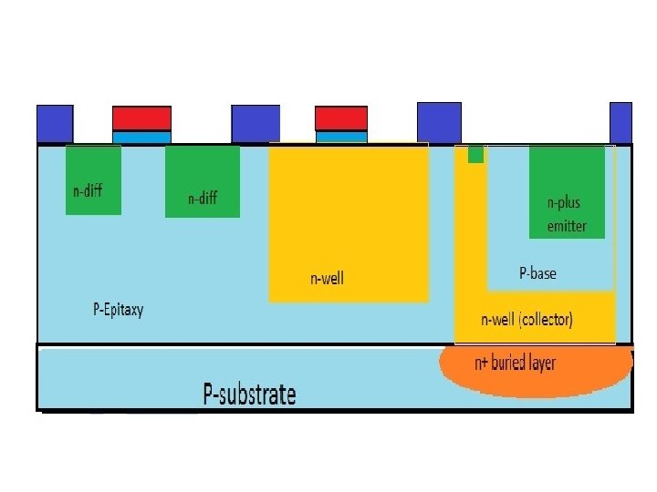
Bi CMOS

SOI

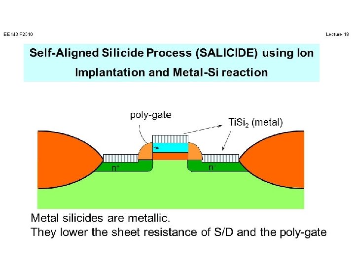
Silicide: A silicide prepared by a self-aligned process is called a salicide. This is a process in which silicide contacts are formed only in those areas in which deposited metal (which after annealing becomes a metal component of the silicide) is in direct contact with silicon, hence, the process is self-aligned. It is commonly implemented in MOS/CMOS processes for ohmic contacts of the source, drain, and poly-Si gate.

Comparison between CMOS & Bi CMOS 1. Low static power dissipation High power dissipation 2. High input impedance Low input impedance 3. Scalable Threshold voltage 4. High noise margin Low voltage swing logic 5. High package density Low package density 6. Low output drive current High output drive current 7. Bidirectional capability Unidirectional 8. Low gm High gm


MOSFET :

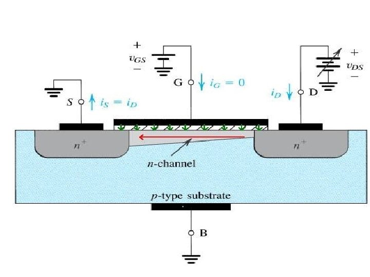
MOSFET Field effect transistor is a unipolar transistor, which acts as a voltage-controlled current device and is a device in which current at two electrodes drain and source is controlled by the action of an electric field at another electrode gate having in-between semiconductor and metal very a thin metal oxide layer.
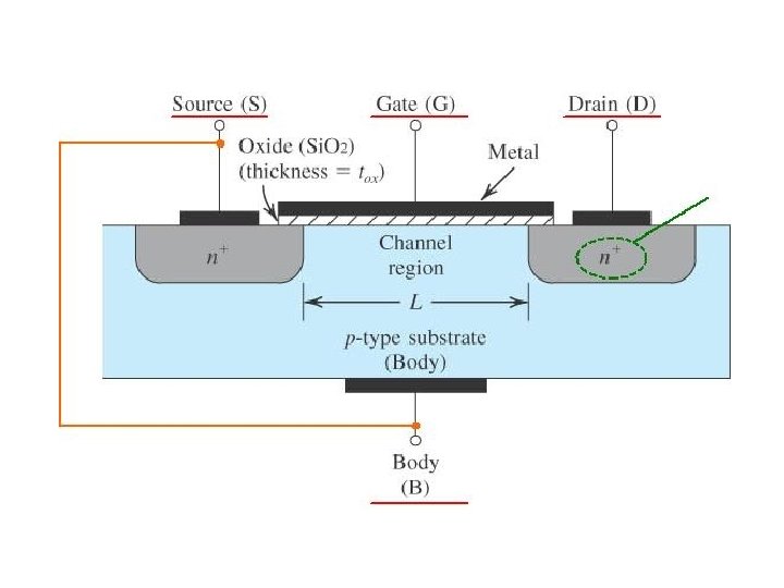

With no bias voltage applied to the gate terminal, there exists two back-to-back pn junctions between the drain and the source. No current flows from drain to source (the resistance will be on the order of 1012 Ω).
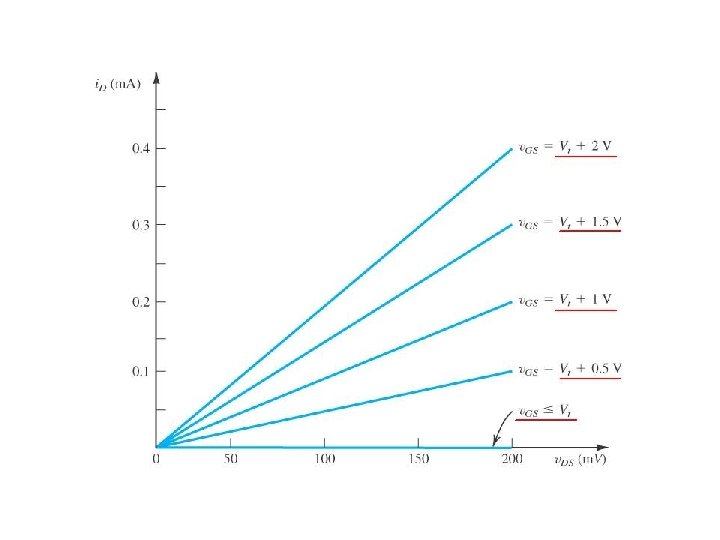

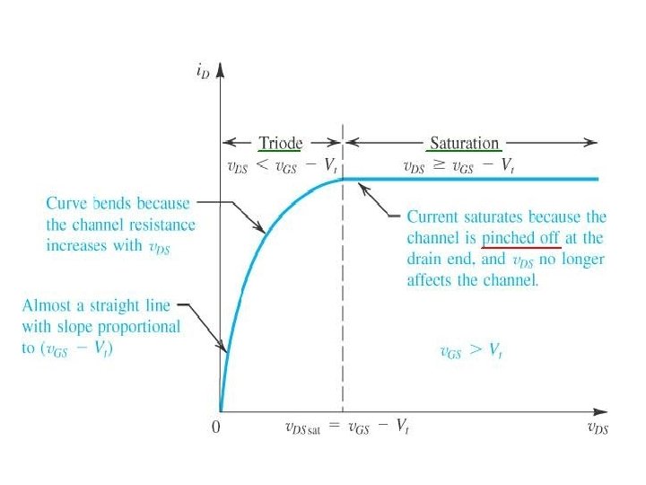
Regions of MOSFET operation • Off or Cutoff region: id =0 i. e v. GS < Vt • Triode region: v. GS > Vt and v. DS < v. DSsat • Saturation region: v. GS > Vt and v. DS >= v. DSsat

Relation between i d Vs VDS :

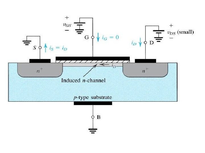
Let L- is the channel length of the transistor. W- is the width of the transistor. D- is the thickness of the oxide layer. ε - is the permittivity of the oxide layer. IDS VDS . - Drain to source current. - Drain to source voltage Q – Charge induced in the channel τ - the electron transit time

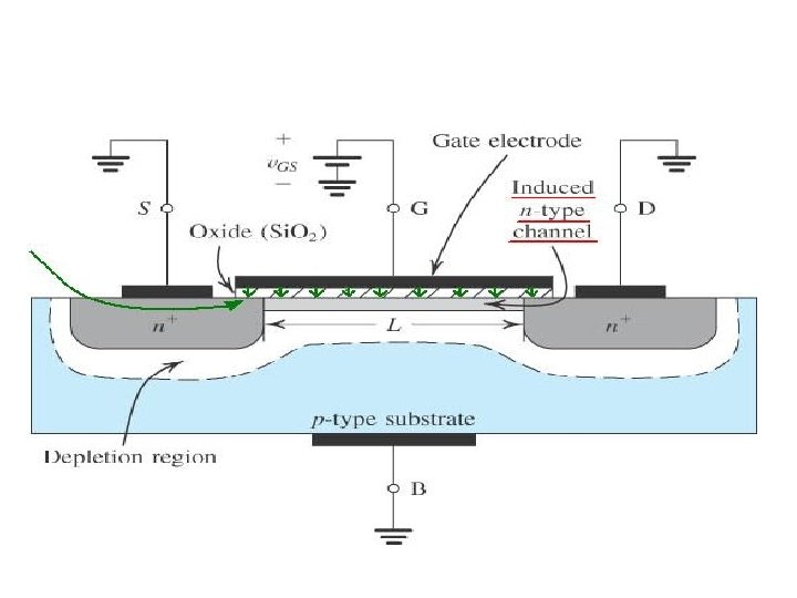
The voltage on Gate induces a charge in the channel between Source and Drain. Which is then moved from source to drain under the influence of electric field created by voltage applied between Drain and Source VDS. Hence the current IDS is given by

Where But the velocity

Where μ = electron mobility or hole mobility EDS = electric field ( drain and source ) now

thus

Non saturated region : Let the charged induced in the channel due to gate voltage is given by Where Eg εins ε 0 -- Charge / unit area Eg – avg. electric field gate to channel εins -- relative permitivity of insulation between gate and channel – 4 for Si 02

ε 0 -- permitivity of free space— 8. 854 x 10 -4 F/cm Since the voltage along the channel varies linearly with distance X from source due to IR drop in the channel, hence the average VDS is and the effective gate voltage Vg =Vgs – Vt

Where D– oxide thickness
 in (3)")
Substitute (4) in (3)

Where But in common practice

We know , gate /channel capacitance Then

In terms of C 0

In saturation , or

MOS Tx. Symbols:

Threshold voltage: The v. GS required to accumulate sufficient numbers of mobile electrons in the channel is called the threshold voltage Vt. For an n-channel MOSFET, Vt ≈1 − 3 V (note that this is a positive voltage).

Threshold voltage: The Threshold voltage, VT for a MOS transistor can be defined as the voltage applied between the gate and the source of the MOS transistor below which the drain to source current, IDS effectively drops to zero. where QB – Charge /unit area in the depleation layerbeneath the oxide

QSS – Charge density at Si : Si. O 2 intearface Cox – Capacitance per unit gate area. ϕms– Work function difference between gate and Si ϕf. N– Fermi level potential between inverted surface and bulk Si. For Poly Si gate and Si substrate the value of ϕms is negative but neglected
 x 10 -8 coulomb/m 2 VSB–")
ϕSS – ( 1. 5 to 8 ) x 10 -8 coulomb/m 2 VSB– Substrate bias voltage q – 1. 6 x 10 -19 coulomb N – Impurity concentration in the substrate N A or ND εSi –relative permittivity of Si- 11. 7 ni – intrinsic concentration-1. 6 x 10¹⁰ /cm 3

K – Boltzmenn’s constant – 1. 4 x 10 -23 J/o K Relation between Vt and Vsb: Considering the body effect i. e increasing Vsb causes the channel to be depleted of charge carriers and thus the threshold voltage is raised. And is given by Where γ is a constant which depends on substrate doping
 is the threshold voltage for Vsb =")
Alternatively , we may write Where Vt(o) is the threshold voltage for Vsb = 0 Typical values for n. MOS enhancement mode transistor Vt = 0. 2 Vdd when Vsb = 0 V Vt = 0. 3 Vdd when Vsb = 5 V

Trans conductance is defined as Trans conductance in terms of transistor parameters:

since

hence

In saturation ,
, it can be increased")
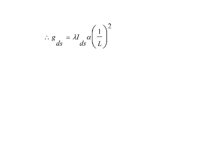
Alternatively Since gm is proportional to width ( W ), it can be increased by increasing width but it increases input capacitance and area occupied. The output conductance g ds can be expressed as

Subthreshold region: For Vgs<Vt also we will get some value of Drain current this is called as Subthreshold current and the region is called as Subthreshold region.

Channel length modulation: The channel length of the MOSFET is changed due to the change in the drain to source voltage. This effect is called as the channel length modulation. The effective channel length & the value of the drain current considering channel length modulation into effect is given by, Where - λ is the channel length modulation factor.

Figure of merit ωo : It shows that switching speed depends on Vg , μ , inversely as the square of channel length and gm.

μn – 1250 cm 2 /V sec μp– 480 cm 2 /V sec

Mobility: Mobility is the defined as the ease with which the charge carriers drift in the substrate material. Mobility decreases with increase in doping concentration and increase in temperature. Mobility is the ratio of average carrier drift velocity and electric field. Mobility is represented by the symbol μ.

Drain punchthough: When the drain is a high voltage, the depletion region around the drain may extend to the source, causing the current to flow even its gate voltage is zero. This is known as Punchthrough condition.

Impact Ionization-hot electrons: When the length of the transistor is reduced, the electric field at the drain increases. The field can become so high that electrons are imparted with enough energy we can term them as hot. These hot electrons impact the drain, dislodging holes that are then swept toward the negatively charged substrate and appear as a substrate current. This effect is known as Impact Ionization.
to")
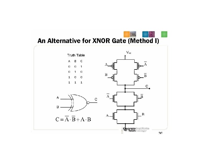
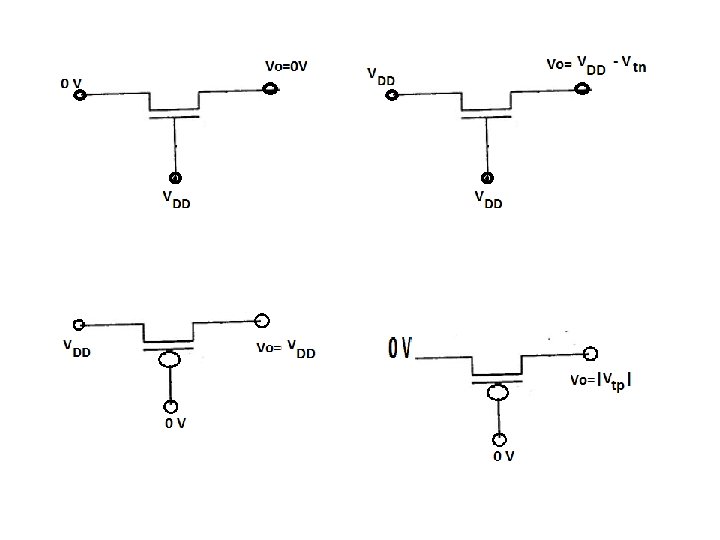
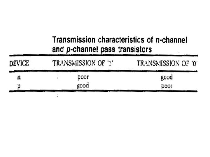
Pass transistor logic : Pass characteristics: passing of voltage from drain ( or source)to source( or drain ) when device is ON (via gate voltage)
 is to be transferred using n. MOS the output will")
If Vdd (5 volts) is to be transferred using n. MOS the output will be (Vdd-Vtn). POOR 1 or Weak Logic 1 If Gnd(0 volts) is to be transferred using n. MOS the output will be Gnd. GOOD 0 or Strong Logic 0 If Vdd (5 volts) is to be transferred using p. MOS the output will be Vdd. GOOD 1 or Strong Logic 1 If Gnd(0 volts) is to be transferred using p. MOS the output will be Vtp. POOR 0 or Weak Logic 0.

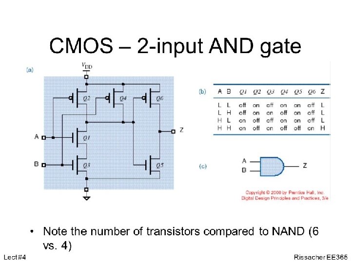
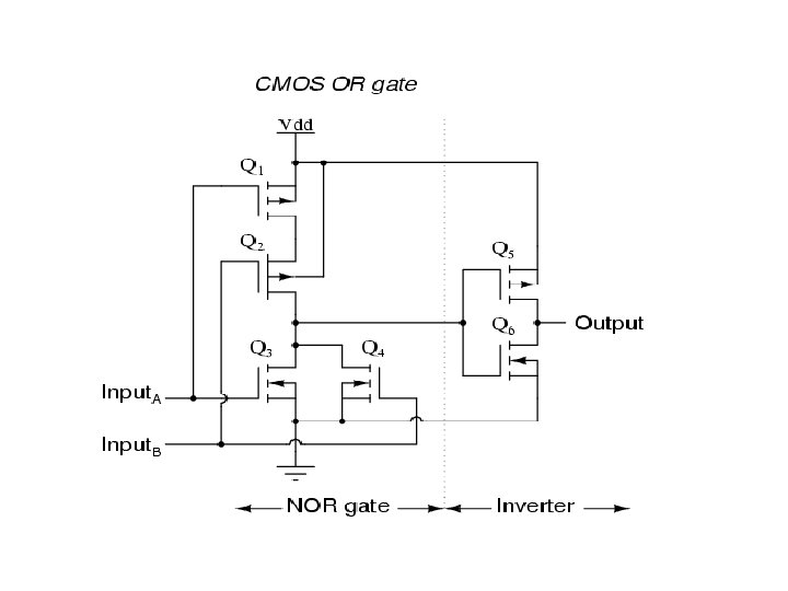
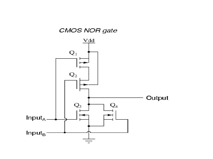
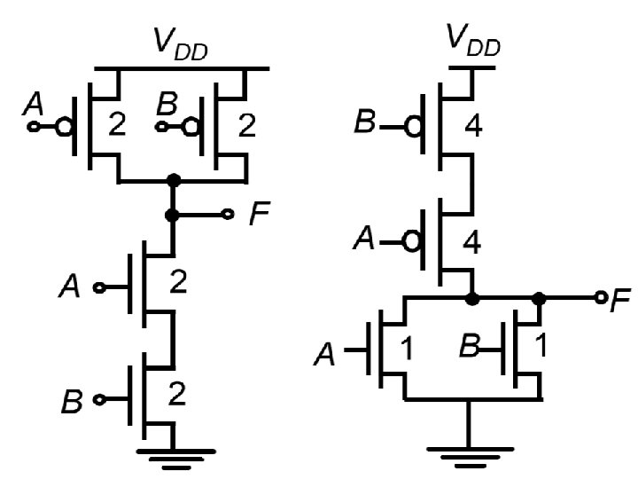
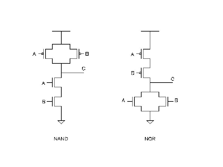
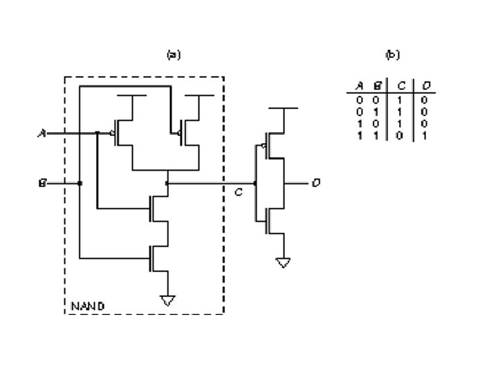
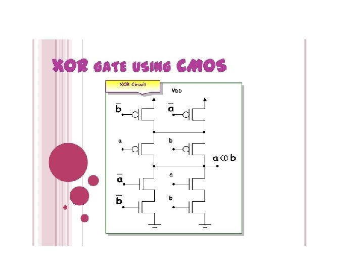
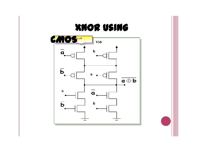
Logic gates using pass transistor logic :

Various forms of Pull Up loads: 1. Resistive load It requires large space 2. Depletion MOSFET 1. Rail to rail current flows when Vin – logic ‘ 1’ 2. Switching of output from 1 to 0 begins when. Vin exceeds Vt of P. D device. 3. Enhancement MOSFET 1. Dissipation is high since current flows when Vin=‘ 1’ 2. Vout can never reach Vdd 3. Two power supplies are required

4. Complementary MOSFET 1. No current flow either for logical 0 or for logical 1 inputs 2. Full logic voltage can be observed

n. MOS Inverter:

Inverter transfer characteristics:

CMOS inverter current Vs Vin

We know , in resistive region in saturation region

in region 3 both the transistors are in ON Where and

Vin in terms β ,

Symmetrycity can be obtained at the above equation can be satisfied when

Bi CMOS inverter

Alternative Bi CMOS inverter with no static current:

Improved Bi. CMOS inverter with better logic levels

Improved Bi. CMOS inverter for base current discharge

CMOS inverter

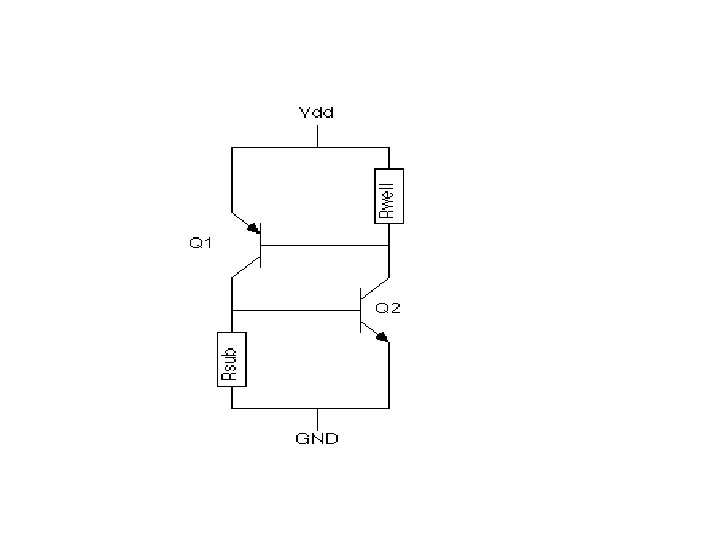
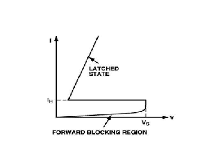
Latch up : Latch-up is a condition in which the parasitic components give rise to the establishment of low resistance conducting paths between Vss and Vss with disastrous results
- Slides: 130