Introduction to CMOS VLSI Design Lecture 1 Circuits

- Slides: 35

Introduction to CMOS VLSI Design Lecture 1: Circuits & Layout Manoel E. de Lima – CIn – UFPE David Harris Harvey Mudd College Spring 2004

Outline q q q CMOS Gate Design Pass Transistors CMOS Latches & Flip-Flops Standard Cell Layouts Stick Diagrams 1: Circuits & Layout CMOS VLSI Design Slide 2

CMOS Gate Design q Activity: – Sketch a 4 -input CMOS NAND gate 1: Circuits & Layout CMOS VLSI Design Slide 3

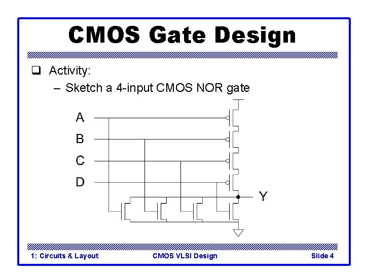
CMOS Gate Design q Activity: – Sketch a 4 -input CMOS NOR gate 1: Circuits & Layout CMOS VLSI Design Slide 4

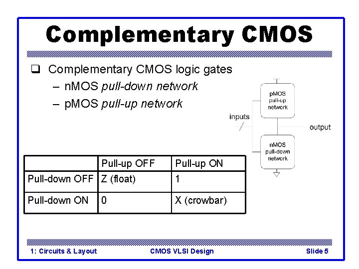
Complementary CMOS q Complementary CMOS logic gates – n. MOS pull-down network – p. MOS pull-up network Pull-up OFF Pull-up ON Pull-down OFF Z (float) 1 Pull-down ON X (crowbar) 1: Circuits & Layout 0 CMOS VLSI Design Slide 5

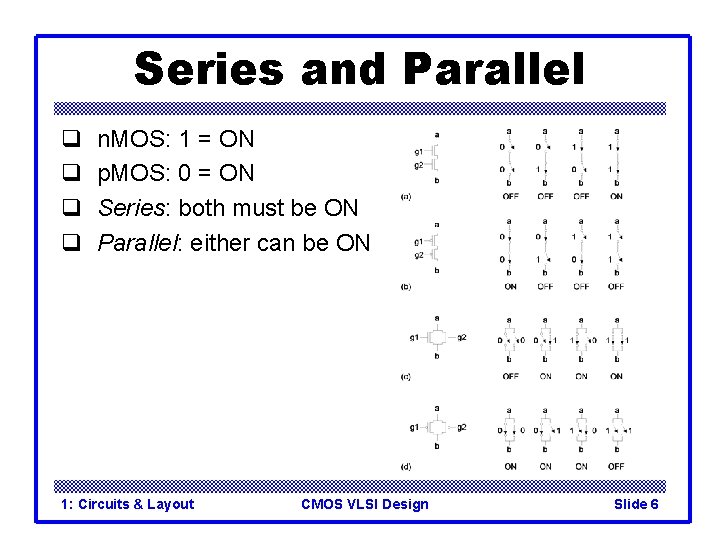
Series and Parallel q q n. MOS: 1 = ON p. MOS: 0 = ON Series: both must be ON Parallel: either can be ON 1: Circuits & Layout CMOS VLSI Design Slide 6

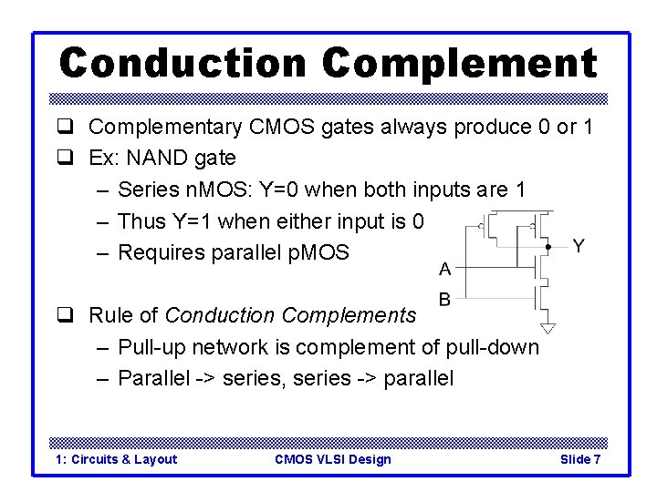
Conduction Complement q Complementary CMOS gates always produce 0 or 1 q Ex: NAND gate – Series n. MOS: Y=0 when both inputs are 1 – Thus Y=1 when either input is 0 – Requires parallel p. MOS q Rule of Conduction Complements – Pull-up network is complement of pull-down – Parallel -> series, series -> parallel 1: Circuits & Layout CMOS VLSI Design Slide 7

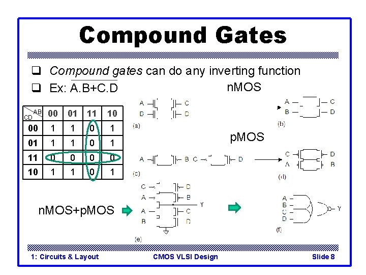
Compound Gates q Compound gates can do any inverting function n. MOS q Ex: A. B+C. D 00 01 11 10 00 1 1 01 1 1 0 1 11 0 0 10 1 1 0 1 CD AB p. MOS n. MOS+p. MOS 1: Circuits & Layout CMOS VLSI Design Slide 8

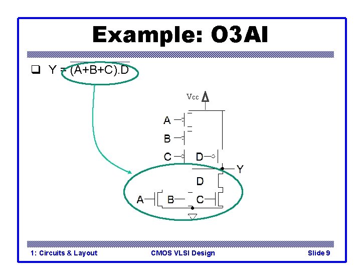
Example: O 3 AI q Y = (A+B+C). D Vcc 1: Circuits & Layout CMOS VLSI Design Slide 9

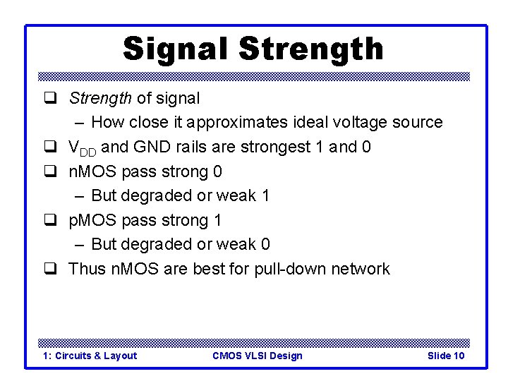
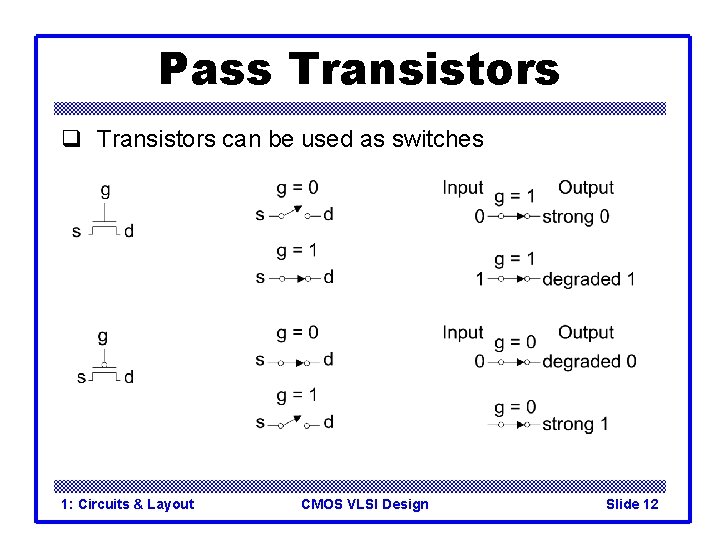
Signal Strength q Strength of signal – How close it approximates ideal voltage source q VDD and GND rails are strongest 1 and 0 q n. MOS pass strong 0 – But degraded or weak 1 q p. MOS pass strong 1 – But degraded or weak 0 q Thus n. MOS are best for pull-down network 1: Circuits & Layout CMOS VLSI Design Slide 10

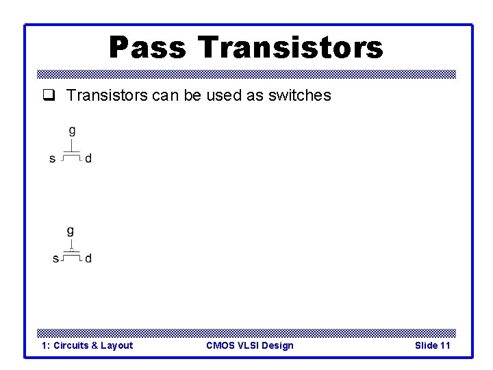
Pass Transistors q Transistors can be used as switches 1: Circuits & Layout CMOS VLSI Design Slide 11

Pass Transistors q Transistors can be used as switches 1: Circuits & Layout CMOS VLSI Design Slide 12

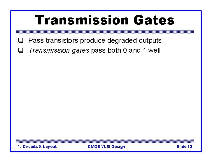
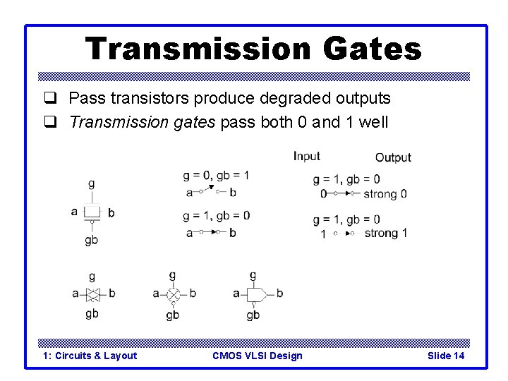
Transmission Gates q Pass transistors produce degraded outputs q Transmission gates pass both 0 and 1 well 1: Circuits & Layout CMOS VLSI Design Slide 13

Transmission Gates q Pass transistors produce degraded outputs q Transmission gates pass both 0 and 1 well 1: Circuits & Layout CMOS VLSI Design Slide 14

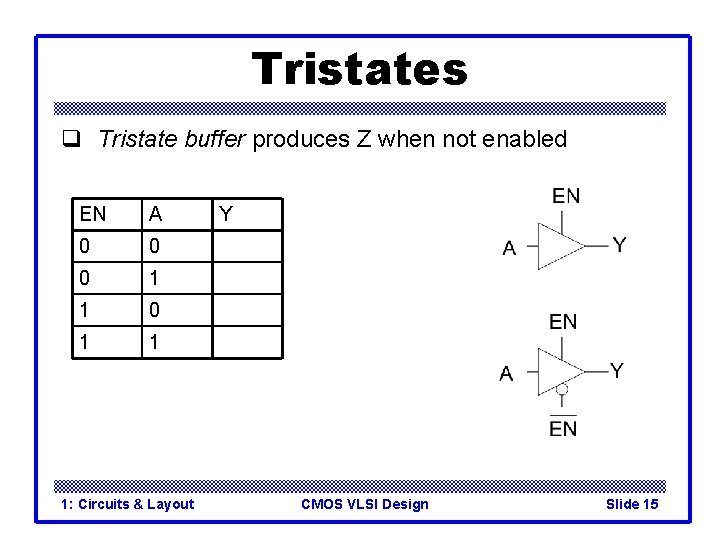
Tristates q Tristate buffer produces Z when not enabled EN A 0 0 0 1 1 1: Circuits & Layout Y CMOS VLSI Design Slide 15

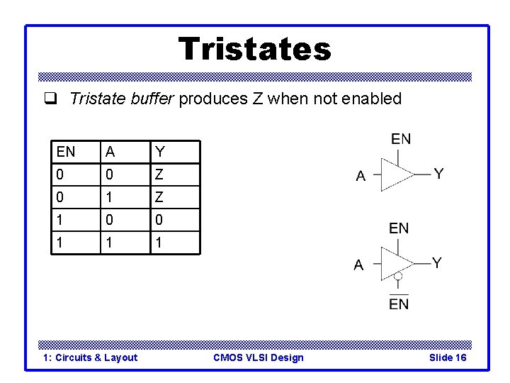
Tristates q Tristate buffer produces Z when not enabled EN A Y 0 0 Z 0 1 Z 1 0 0 1 1: Circuits & Layout CMOS VLSI Design Slide 16

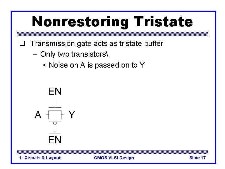
Nonrestoring Tristate q Transmission gate acts as tristate buffer – Only two transistors • Noise on A is passed on to Y 1: Circuits & Layout CMOS VLSI Design Slide 17

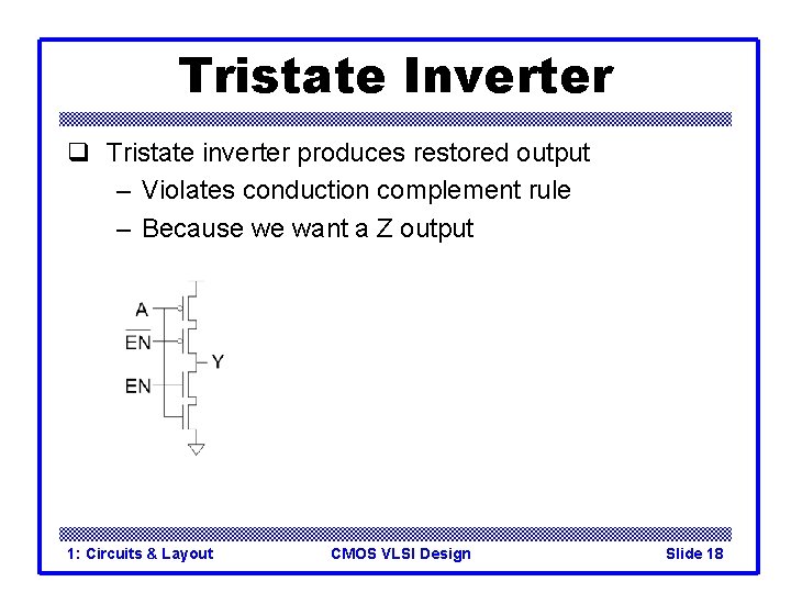
Tristate Inverter q Tristate inverter produces restored output – Violates conduction complement rule – Because we want a Z output 1: Circuits & Layout CMOS VLSI Design Slide 18

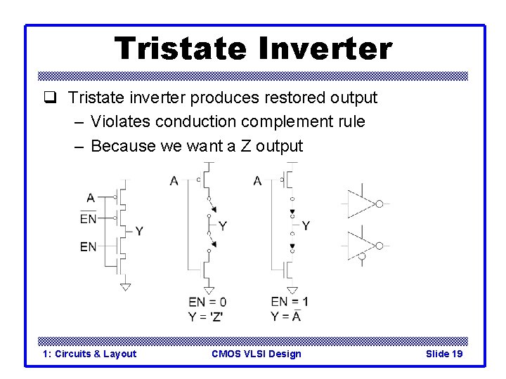
Tristate Inverter q Tristate inverter produces restored output – Violates conduction complement rule – Because we want a Z output 1: Circuits & Layout CMOS VLSI Design Slide 19

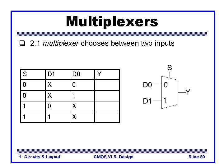
Multiplexers q 2: 1 multiplexer chooses between two inputs S D 1 D 0 0 X 1 1 X 1: Circuits & Layout Y CMOS VLSI Design Slide 20

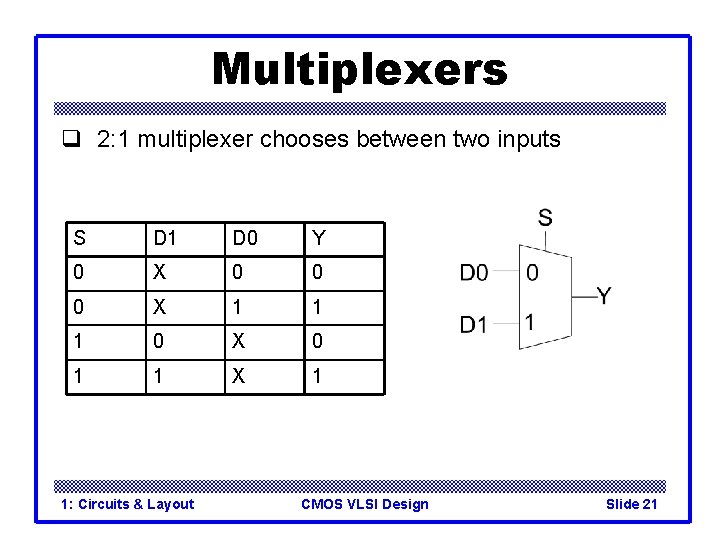
Multiplexers q 2: 1 multiplexer chooses between two inputs S D 1 D 0 Y 0 X 0 0 0 X 1 1 1 0 X 0 1 1 X 1 1: Circuits & Layout CMOS VLSI Design Slide 21

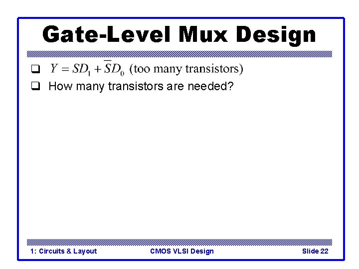
Gate-Level Mux Design q q How many transistors are needed? 1: Circuits & Layout CMOS VLSI Design Slide 22

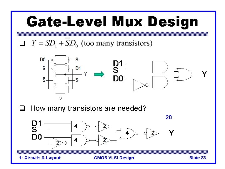
Gate-Level Mux Design q q How many transistors are needed? 20 1: Circuits & Layout CMOS VLSI Design Slide 23

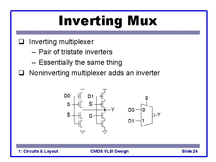
Inverting Mux q Inverting multiplexer – Pair of tristate inverters – Essentially the same thing q Noninverting multiplexer adds an inverter 1: Circuits & Layout CMOS VLSI Design Slide 24

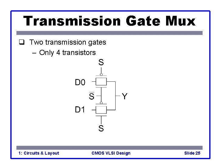
Transmission Gate Mux q Two transmission gates – Only 4 transistors 1: Circuits & Layout CMOS VLSI Design Slide 25

4: 1 Multiplexer q 4: 1 mux chooses one of 4 inputs using two selects 1: Circuits & Layout CMOS VLSI Design Slide 26

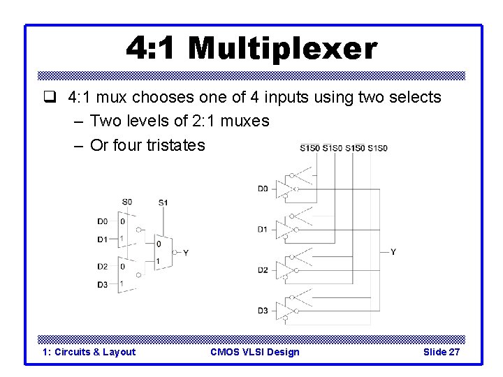
4: 1 Multiplexer q 4: 1 mux chooses one of 4 inputs using two selects – Two levels of 2: 1 muxes – Or four tristates 1: Circuits & Layout CMOS VLSI Design Slide 27

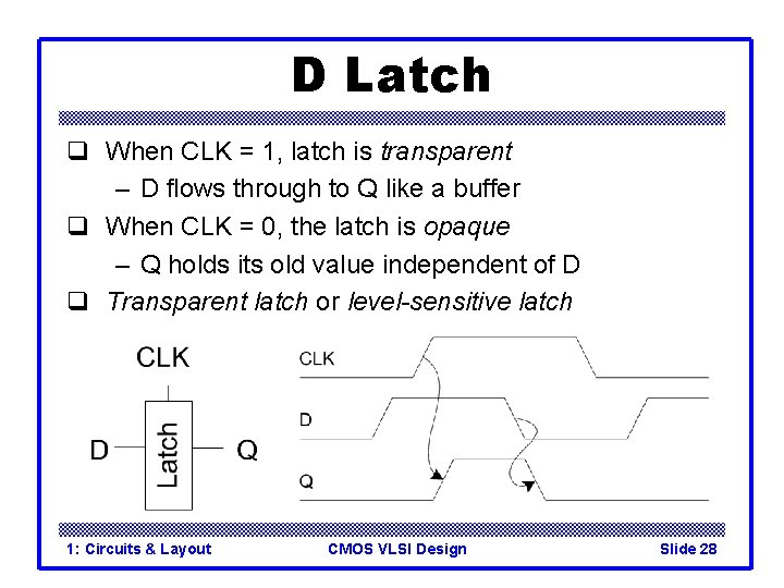
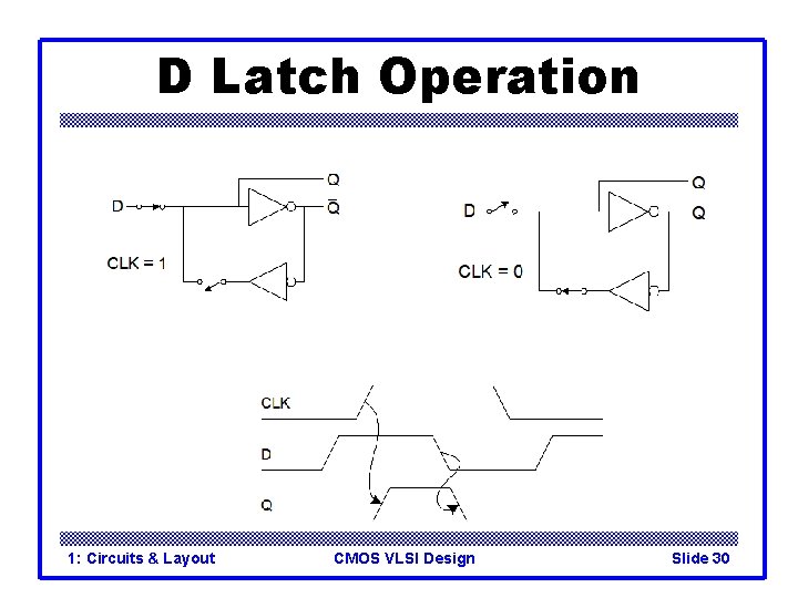
D Latch q When CLK = 1, latch is transparent – D flows through to Q like a buffer q When CLK = 0, the latch is opaque – Q holds its old value independent of D q Transparent latch or level-sensitive latch 1: Circuits & Layout CMOS VLSI Design Slide 28

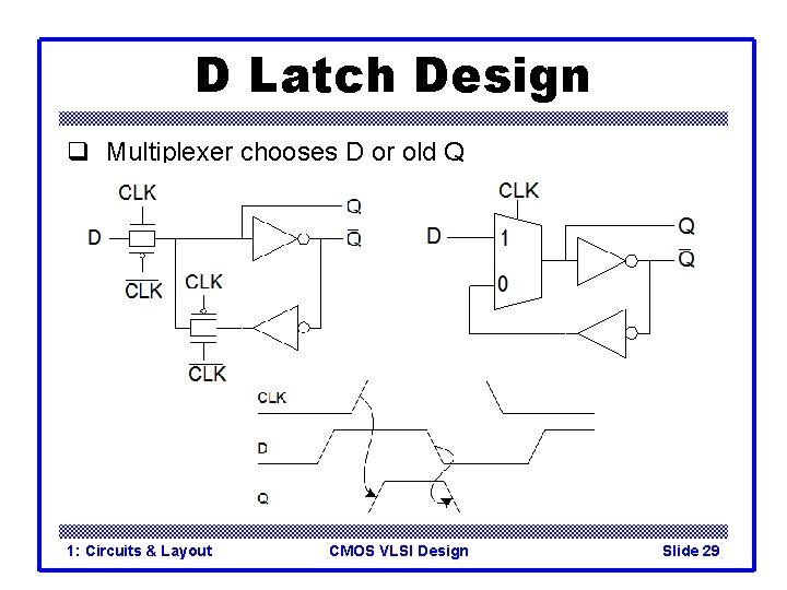
D Latch Design q Multiplexer chooses D or old Q 1: Circuits & Layout CMOS VLSI Design Slide 29

D Latch Operation 1: Circuits & Layout CMOS VLSI Design Slide 30

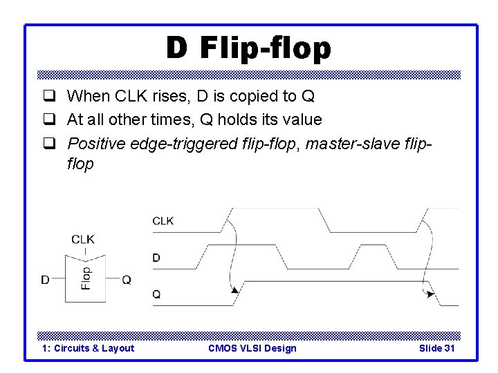
D Flip-flop q When CLK rises, D is copied to Q q At all other times, Q holds its value q Positive edge-triggered flip-flop, master-slave flipflop 1: Circuits & Layout CMOS VLSI Design Slide 31

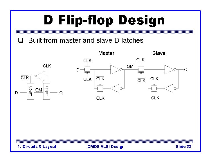
D Flip-flop Design q Built from master and slave D latches Master 1: Circuits & Layout CMOS VLSI Design Slave Slide 32

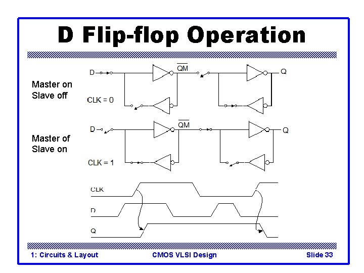
D Flip-flop Operation Master on Slave off Master of Slave on 1: Circuits & Layout CMOS VLSI Design Slide 33

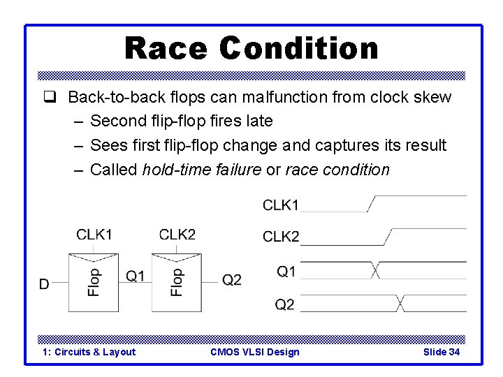
Race Condition q Back-to-back flops can malfunction from clock skew – Second flip-flop fires late – Sees first flip-flop change and captures its result – Called hold-time failure or race condition 1: Circuits & Layout CMOS VLSI Design Slide 34

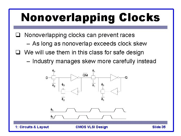
Nonoverlapping Clocks q Nonoverlapping clocks can prevent races – As long as nonoverlap exceeds clock skew q We will use them in this class for safe design – Industry manages skew more carefully instead 1: Circuits & Layout CMOS VLSI Design Slide 35