LDIC Course Contents n Unit 1 Operational Amplifier



- Slides: 103

LDIC Course Contents n Unit 1 - Operational Amplifier n Unit 2 - Applications of OP-Amp n Unit 3 - Oscillators n Unit 4 - D-A and A-D Converters n Unit 5 - Logic Families n Unit 6 - Memories

Text Books: 1. Linear Integrated Circuits – D. Roy Choudhury 2. Op-Amps & Linear ICs – Ramakanth A. Gayakwad. 3. Digital Fundamentals – Floyd and Jain

Unit 1 - Operational amplifies n What is an Integrated Circuit? n Where do you use an Integrated Circuit? n Why do you prefer an Integrated Circuit to the circuits made by interconnecting discrete components?

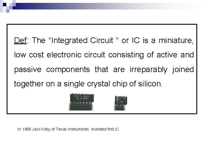
Def: The “Integrated Circuit “ or IC is a miniature, low cost electronic circuit consisting of active and passive components that are irreparably joined together on a single crystal chip of silicon. In 1958 Jack Kilby of Texas Instruments invented first IC

Applications of an Integrated Circuit n Communication n Control n Instrumentation n Computer n Electronics

Advantages: n Small size n Low cost n Less weight n Low supply voltages n Low power consumption n Highly reliable n Matched devices n Fast speed

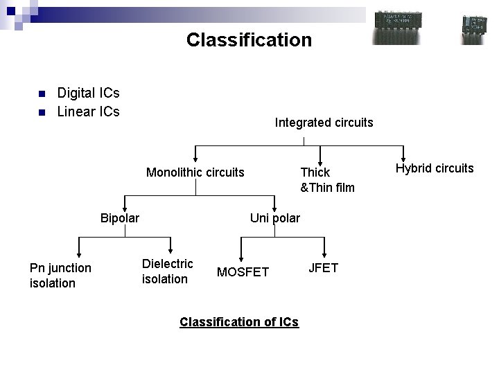
Classification n n Digital ICs Linear ICs Integrated circuits Monolithic circuits Bipolar Pn junction isolation Thick &Thin film Uni polar Dielectric isolation MOSFET Classification of ICs JFET Hybrid circuits

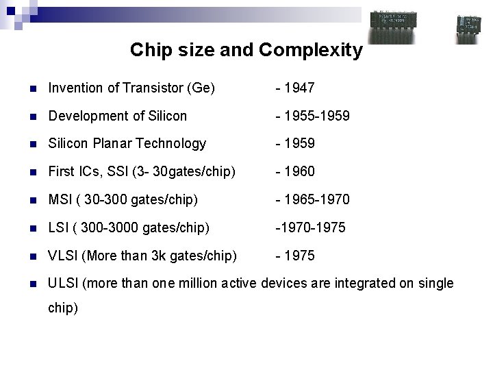
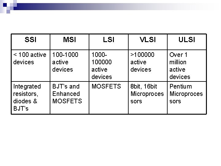
Chip size and Complexity n Invention of Transistor (Ge) - 1947 n Development of Silicon - 1955 -1959 n Silicon Planar Technology - 1959 n First ICs, SSI (3 - 30 gates/chip) - 1960 n MSI ( 30 -300 gates/chip) - 1965 -1970 n LSI ( 300 -3000 gates/chip) -1970 -1975 n VLSI (More than 3 k gates/chip) - 1975 n ULSI (more than one million active devices are integrated on single chip)

SSI MSI LSI VLSI ULSI < 100 active 100 -1000 devices active devices 100000 active devices >100000 active devices Integrated resistors, diodes & BJT’s MOSFETS 8 bit, 16 bit Pentium Microproces sors BJT’s and Enhanced MOSFETS Over 1 million active devices

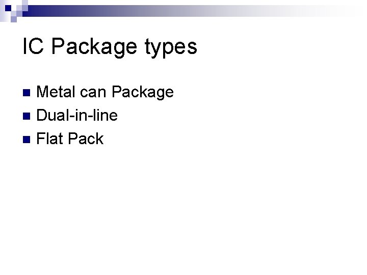
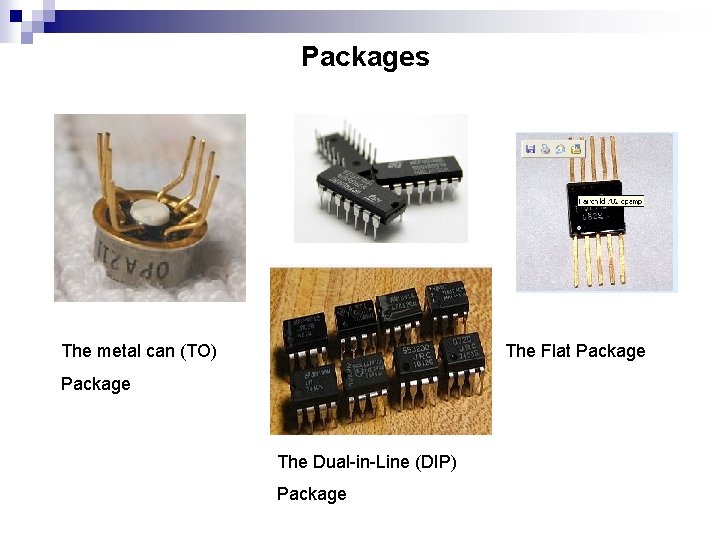
IC Package types Metal can Package n Dual-in-line n Flat Pack n

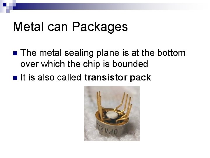
Metal can Packages The metal sealing plane is at the bottom over which the chip is bounded n It is also called transistor pack n

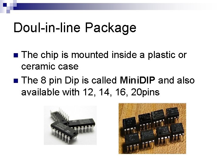
Doul-in-line Package The chip is mounted inside a plastic or ceramic case n The 8 pin Dip is called Mini. DIP and also available with 12, 14, 16, 20 pins n

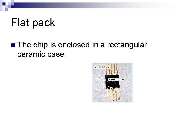
Flat pack n The chip is enclosed in a rectangular ceramic case

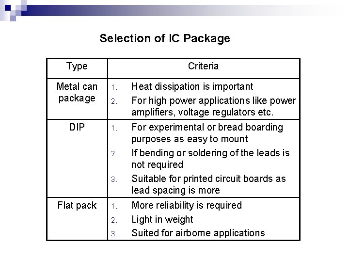
Selection of IC Package Type Criteria Metal can package 1. DIP 1. 2. 3. Flat pack 1. 2. 3. Heat dissipation is important For high power applications like power amplifiers, voltage regulators etc. For experimental or bread boarding purposes as easy to mount If bending or soldering of the leads is not required Suitable for printed circuit boards as lead spacing is more More reliability is required Light in weight Suited for airborne applications

Packages The metal can (TO) The Flat Package The Dual-in-Line (DIP) Package

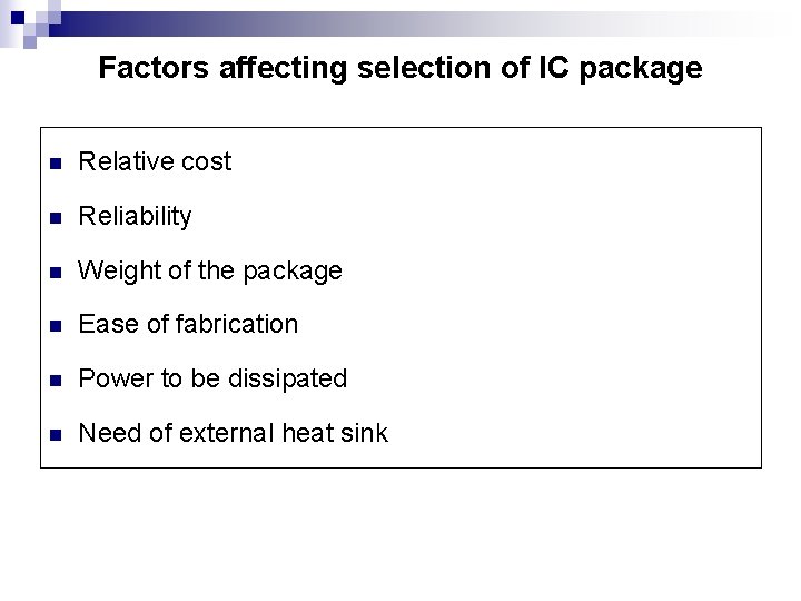
Factors affecting selection of IC package n Relative cost n Reliability n Weight of the package n Ease of fabrication n Power to be dissipated n Need of external heat sink

Temperature Ranges 1. Military temperature range : -55 o C to +125 o C (-55 o C to +85 o C) 2. Industrial temperature range : -20 o C to +85 o C (-40 o C to +85 o C ) 3. Commercial temperature range: 0 o C to +70 o C (0 o C to +75 o C )

Manufacturer’s Designation for Linear ICs n Fairchild - µA, µAF n National Semiconductor - LM, LH, LF, TBA n Motorola - MC, MFC n RCA - CA, CD n Texas Instruments - SN n Signetics - N/S, NE/SE n Burr- Brown - BB

Operational Amplifier An “Operational amplifier” is a direct coupled high-gain amplifier usually consisting of one or more differential amplifiers and usually followed by a level translator and output stage. The operational amplifier is a versatile device that can be used to amplify dc as well as ac input signals and was originally designed for computing such mathematical functions as addition, subtraction, multiplication and integration.

Op Amp Positive power supply (Positive rail) Non-inverting Input terminal Output terminal Inverting input terminal Negative power supply (Negative rail)

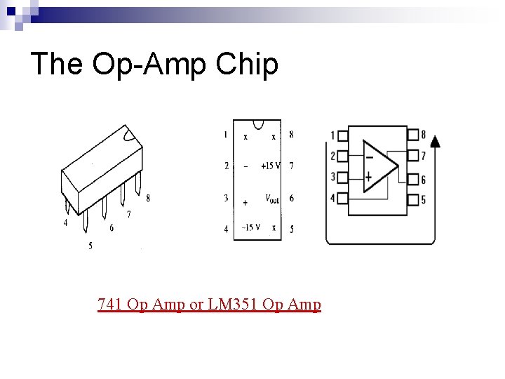
The Op-Amp Chip 741 Op Amp or LM 351 Op Amp

n Op-amp have 5 basic terminals(ie 2 i/p’s 1 o/p and 2 power supply terminals n n The output goes positive when the noninverting input (+) goes more positive than the inverting (-) input, and vice versa.

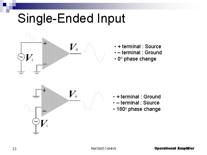
Single-Ended Input • + terminal : Source • – terminal : Ground • 0 o phase change • + terminal : Ground • – terminal : Source • 180 o phase change 23 Ref: 080114 HKN Operational Amplifier

Basic Information of Op-Amp Op-amps have five basic terminals, that is, two input terminals, one output terminal and two power supply terminals.

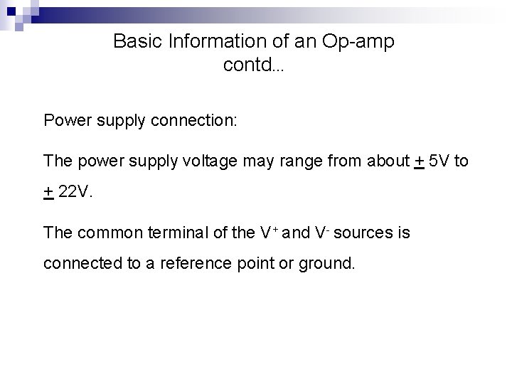
Basic Information of an Op-amp contd… Power supply connection: The power supply voltage may range from about + 5 V to + 22 V. The common terminal of the V+ and V- sources is connected to a reference point or ground.

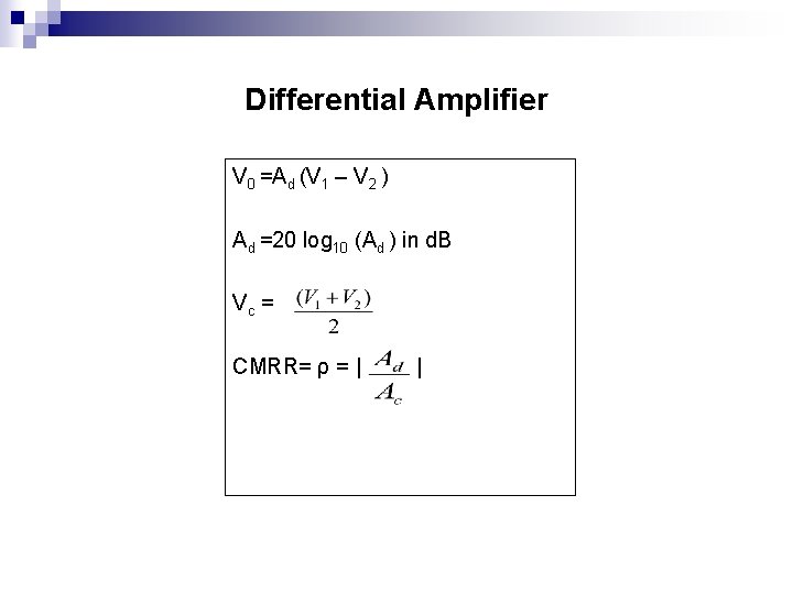
Differential Amplifier V 0 =Ad (V 1 – V 2 ) Ad =20 log 10 (Ad ) in d. B Vc = CMRR= ρ = | |

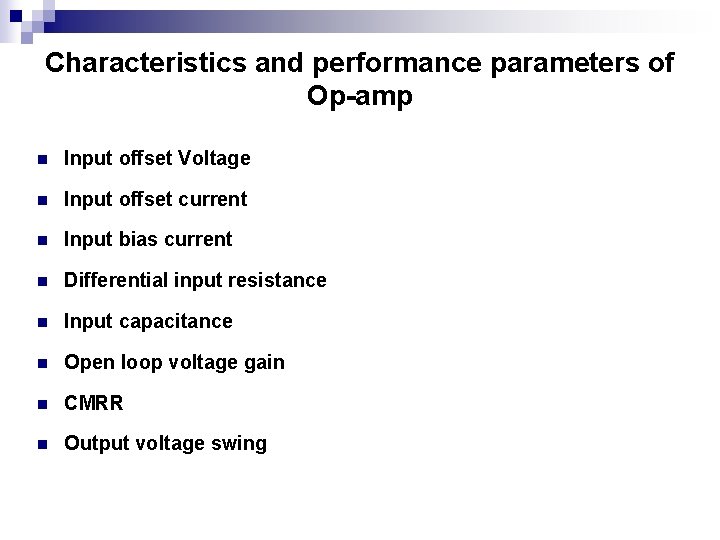
Characteristics and performance parameters of Op-amp n Input offset Voltage n Input offset current n Input bias current n Differential input resistance n Input capacitance n Open loop voltage gain n CMRR n Output voltage swing

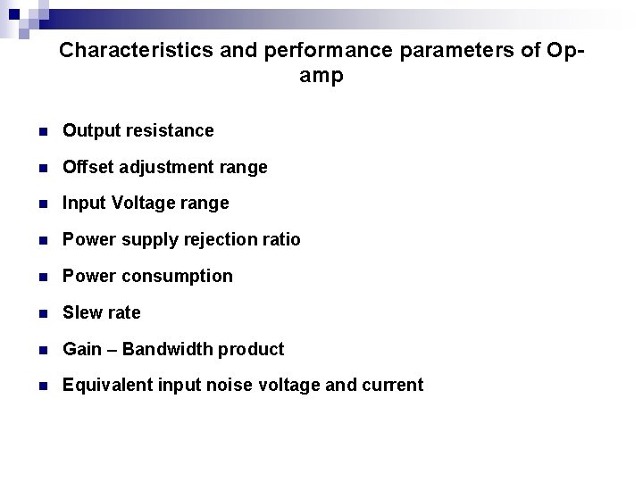
Characteristics and performance parameters of Opamp n Output resistance n Offset adjustment range n Input Voltage range n Power supply rejection ratio n Power consumption n Slew rate n Gain – Bandwidth product n Equivalent input noise voltage and current

Characteristics and performance parameters of Opamp n Average temperature coefficient of offset parameters n Output offset voltage n Supply current

1. Input Offset Voltage The differential voltage that must be applied between the two input terminals of an op-amp, to make the output voltage zero. It is denoted as Vios For op-amp 741 C the input offset voltage is 6 m. V

2. Input offset current The algebraic difference between the currents flowing into the two input terminals of the op-amp It is denoted as Iios = | Ib 1 – Ib 2| For op-amp 741 C the input offset current is 200 n. A

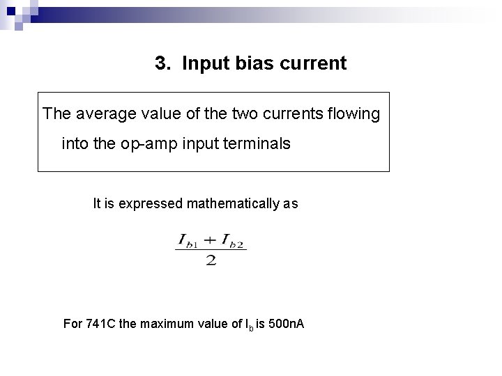
3. Input bias current The average value of the two currents flowing into the op-amp input terminals It is expressed mathematically as For 741 C the maximum value of Ib is 500 n. A

4. Differential Input Resistance It is the equivalent resistance measured at either the inverting or non-inverting input terminal with the other input terminal grounded It is denoted as Ri For 741 C it is of the order of 2 MΩ

5. Input capacitance It is the equivalent capacitance measured at either the inverting or non- inverting input terminal with the other input terminal grounded. It is denoted as Ci For 741 C it is of the 1 -4 p. F

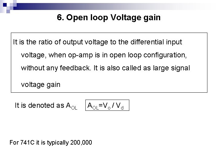
6. Open loop Voltage gain It is the ratio of output voltage to the differential input voltage, when op-amp is in open loop configuration, without any feedback. It is also called as large signal voltage gain It is denoted as AOL=Vo / Vd For 741 C it is typically 200, 000

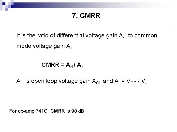
7. CMRR It is the ratio of differential voltage gain Ad to common mode voltage gain Ac CMRR = Ad / Ac Ad is open loop voltage gain AOL and Ac = VOC / Vc For op-amp 741 C CMRR is 90 d. B

8. Output Voltage swing The op-amp output voltage gets saturated at +Vcc and – VEE and it cannot produce output voltage more than +Vcc and –VEE. Practically voltages +Vsat and –Vsat are slightly less than +Vcc and –VEE. For op-amp 741 C the saturation voltages are + 13 V for supply voltages + 15 V

9. Output Resistance It is the equivalent resistance measured between the output terminal of the op-amp and ground It is denoted as Ro For op-amp 741 it is 75Ω

10. Offset voltage adjustment range The range for which input offset voltage can be adjusted using the potentiometer so as to reduce output to zero For op-amp 741 C it is + 15 m. V

11. Input Voltage range It is the range of common mode voltages which can be applied for which op-amp functions properly and given offset specifications apply for the op-amp For + 15 V supply voltages, the input voltage range is + 13 V

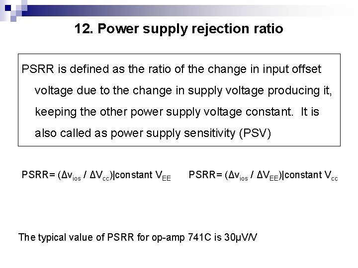
12. Power supply rejection ratio PSRR is defined as the ratio of the change in input offset voltage due to the change in supply voltage producing it, keeping the other power supply voltage constant. It is also called as power supply sensitivity (PSV) PSRR= (Δvios / ΔVcc)|constant VEE PSRR= (Δvios / ΔVEE)|constant Vcc The typical value of PSRR for op-amp 741 C is 30µV/V

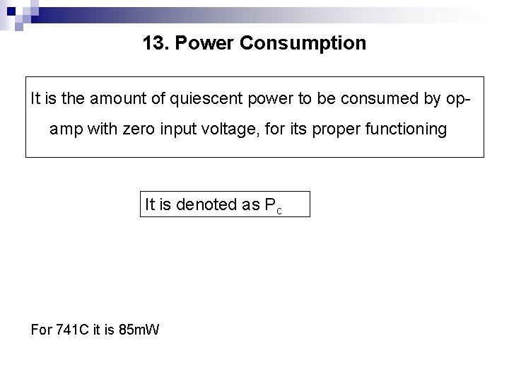
13. Power Consumption It is the amount of quiescent power to be consumed by opamp with zero input voltage, for its proper functioning It is denoted as Pc For 741 C it is 85 m. W

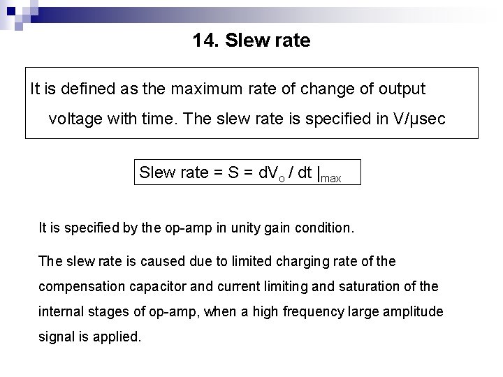
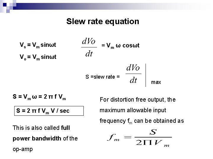
14. Slew rate It is defined as the maximum rate of change of output voltage with time. The slew rate is specified in V/µsec Slew rate = S = d. Vo / dt |max It is specified by the op-amp in unity gain condition. The slew rate is caused due to limited charging rate of the compensation capacitor and current limiting and saturation of the internal stages of op-amp, when a high frequency large amplitude signal is applied.

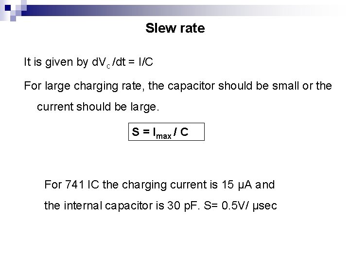
Slew rate It is given by d. Vc /dt = I/C For large charging rate, the capacitor should be small or the current should be large. S = Imax / C For 741 IC the charging current is 15 µA and the internal capacitor is 30 p. F. S= 0. 5 V/ µsec

Slew rate equation Vs = Vm sinωt = Vm ω cosωt Vo = Vm sinωt S =slew rate = S = Vm ω = 2 π f Vm S = 2 π f Vm V / sec This is also called full power bandwidth of the op-amp max For distortion free output, the maximum allowable input frequency fm can be obtained as

15. Gain – Bandwidth product It is the bandwidth of op-amp when voltage gain is unity (1). It is denoted as GB. The GB is also called unity gain bandwidth (UGB) or closed loop bandwidth It is about 1 MHz for op-amp 741 C

16. Equivalent Input Noise Voltage and Current The noise is expressed as a power density Thus equivalent noise voltage is expressed as V 2 /Hz while the equivalent noise current is expressed as A 2 /Hz

17. Average temperature coefficient of offset parameters The average rate of change of input offset voltage per unit change in temperature is called average temperature coefficient of input offset voltage or input offset voltage drift It is measured in µV/o. C. For 741 C it is 0. 5 µV/o. C The average rate of change of input offset current per unit change in temperature is called average temperature coefficient of input offset current or input offset current drift It is measured in n. A/o. C or p. A/o. C. For 741 C it is 12 p. A/o. C

18. Output offset voltage ( Voos ) The output offset voltage is the dc voltage present at the output terminals when both the input terminals are grounded. It is denoted as Voos

19. Supply current It is drawn by the op-amp from the power supply For op-amp 741 C it is 2. 8 m. A

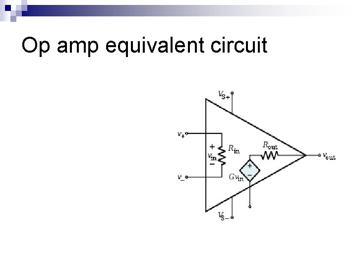
Op amp equivalent circuit

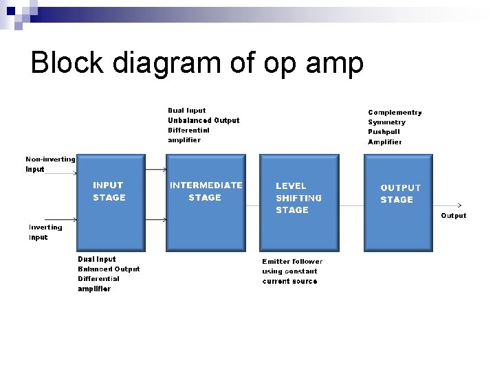
Block diagram of op amp

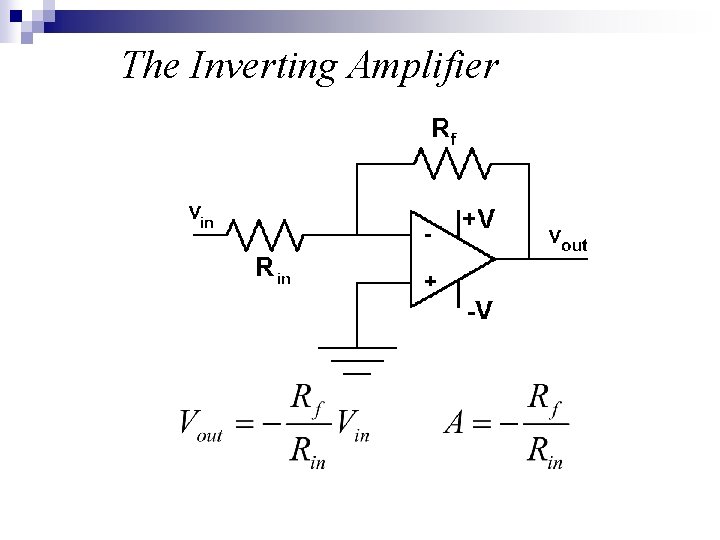
The Inverting Amplifier

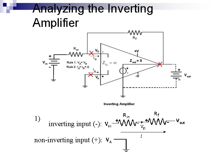
Analyzing the Inverting Amplifier 1) inverting input (-): non-inverting input (+):

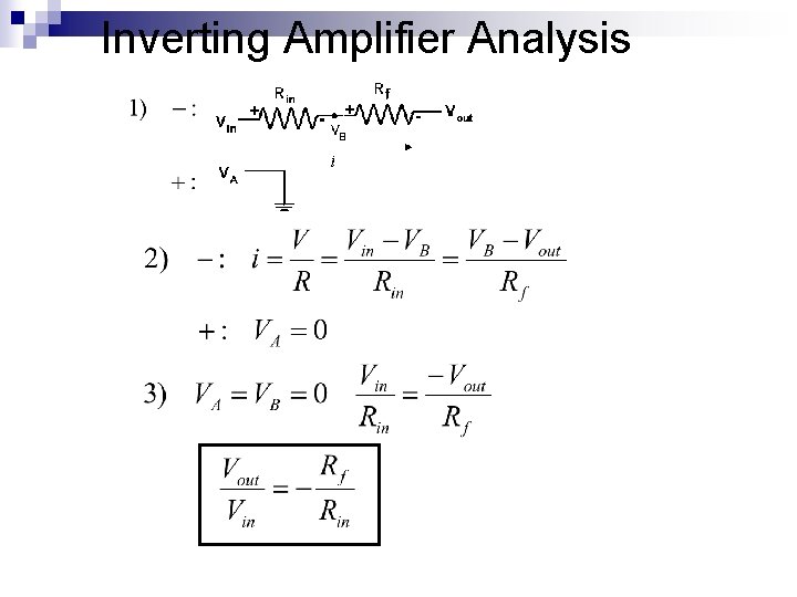
Inverting Amplifier Analysis

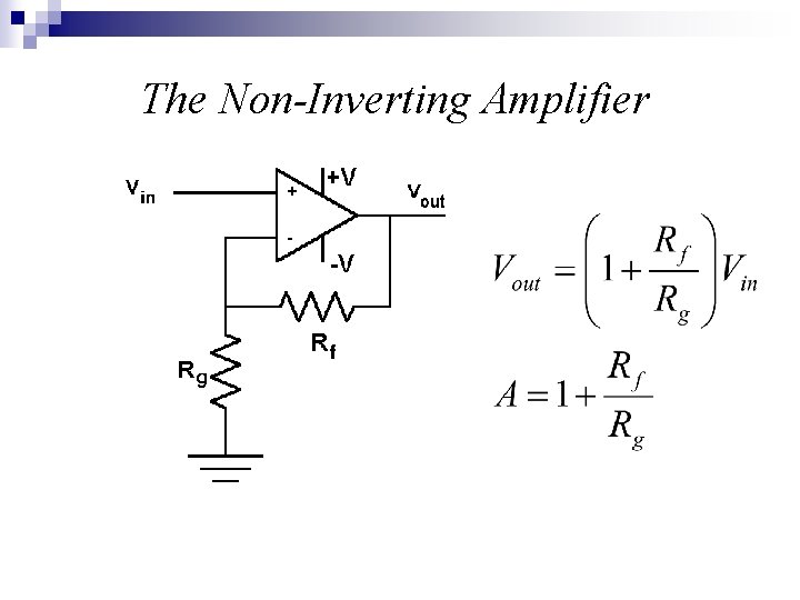
The Non-Inverting Amplifier

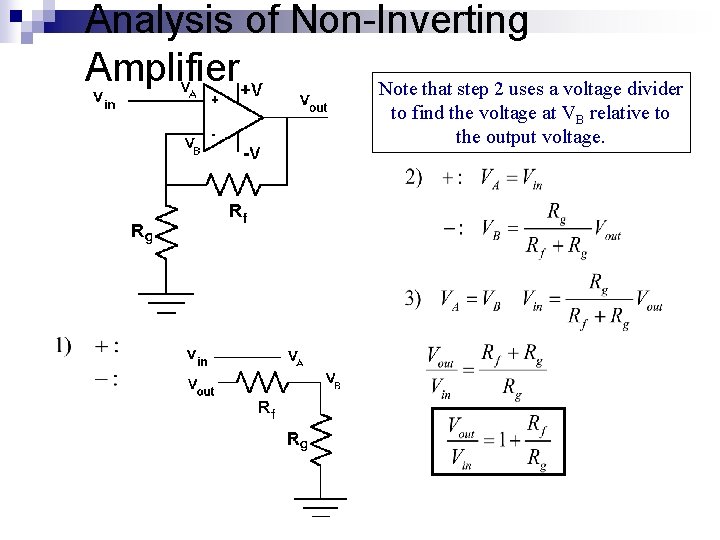
Analysis of Non-Inverting Amplifier Note that step 2 uses a voltage divider to find the voltage at VB relative to the output voltage.

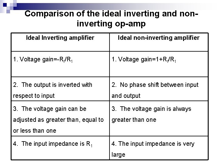
Comparison of the ideal inverting and noninverting op-amp Ideal Inverting amplifier Ideal non-inverting amplifier 1. Voltage gain=-Rf/R 1 1. Voltage gain=1+Rf/R 1 2. The output is inverted with 2. No phase shift between input respect to input and output 3. The voltage gain can be 3. The voltage gain is always adjusted as greater than, equal to greater than one or less than one 4. The input impedance is R 1 4. The input impedance is very large

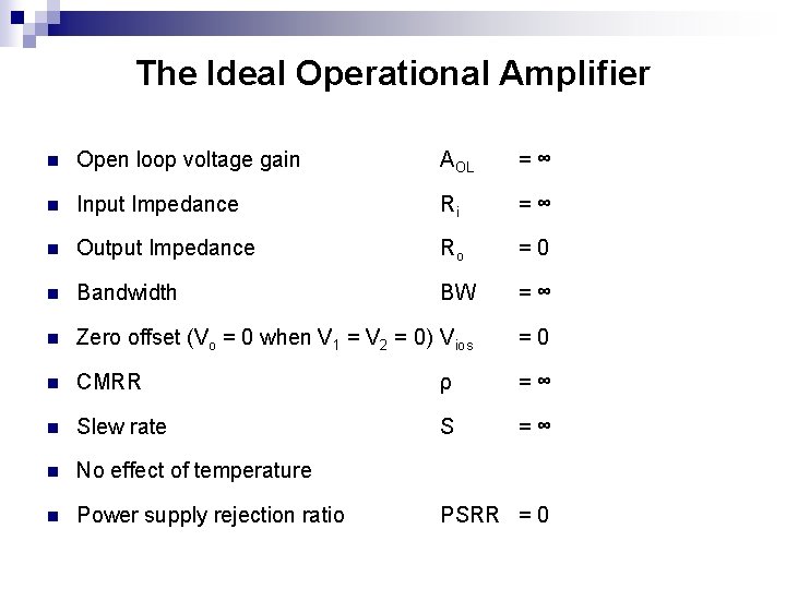
The Ideal Operational Amplifier n Open loop voltage gain AOL =∞ n Input Impedance Ri =∞ n Output Impedance Ro =0 n Bandwidth BW =∞ n Zero offset (Vo = 0 when V 1 = V 2 = 0) Vios =0 n CMRR ρ =∞ n Slew rate S =∞ n No effect of temperature n Power supply rejection ratio PSRR = 0

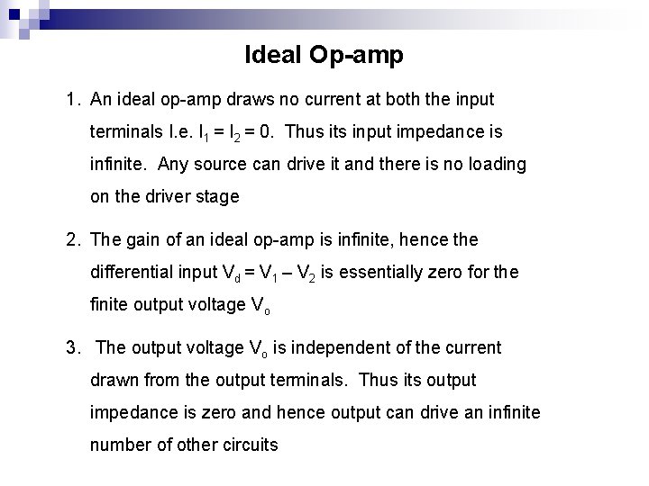
Ideal Op-amp 1. An ideal op-amp draws no current at both the input terminals I. e. I 1 = I 2 = 0. Thus its input impedance is infinite. Any source can drive it and there is no loading on the driver stage 2. The gain of an ideal op-amp is infinite, hence the differential input Vd = V 1 – V 2 is essentially zero for the finite output voltage Vo 3. The output voltage Vo is independent of the current drawn from the output terminals. Thus its output impedance is zero and hence output can drive an infinite number of other circuits

Op-amp Characteristics n DC Characteristics Input bias current Input offset voltage Thermal drift n AC Characteristics Slew rate Frequency response

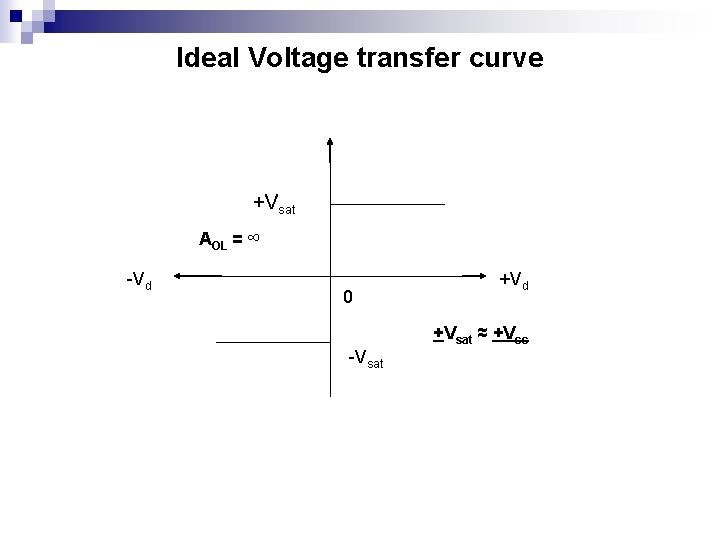
Ideal Voltage transfer curve +Vsat AOL = ∞ -Vd 0 +Vd +Vsat ≈ +Vcc -Vsat

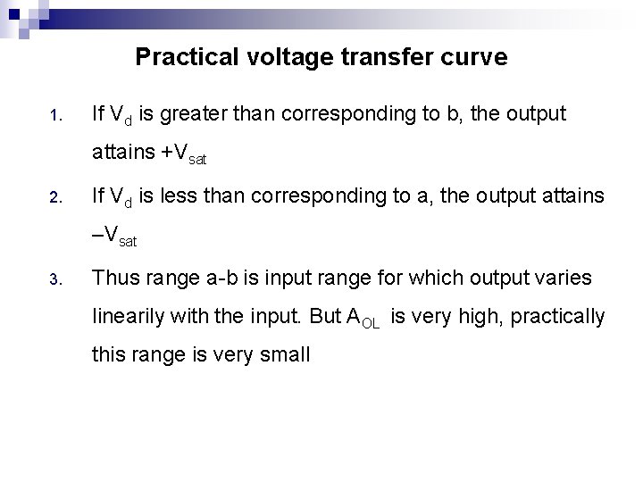
Practical voltage transfer curve 1. If Vd is greater than corresponding to b, the output attains +Vsat 2. If Vd is less than corresponding to a, the output attains –Vsat 3. Thus range a-b is input range for which output varies linearily with the input. But AOL is very high, practically this range is very small

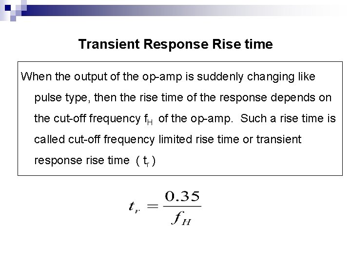
Transient Response Rise time When the output of the op-amp is suddenly changing like pulse type, then the rise time of the response depends on the cut-off frequency f. H of the op-amp. Such a rise time is called cut-off frequency limited rise time or transient response rise time ( tr )

Op-amp Characteristics n DC Characteristics Input bias current Input offset voltage Thermal drift n AC Characteristics Slew rate Frequency response

DC Characteristics Thermal Drift The op-amp parameters input offset voltage Vios and input offset current Iios are not constants but vary with the factors 1. Temperature 2. Supply Voltage changes 3. Time

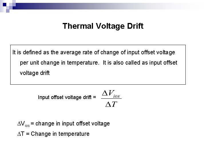
Thermal Voltage Drift It is defined as the average rate of change of input offset voltage per unit change in temperature. It is also called as input offset voltage drift Input offset voltage drift = ∆Vios = change in input offset voltage ∆T = Change in temperature

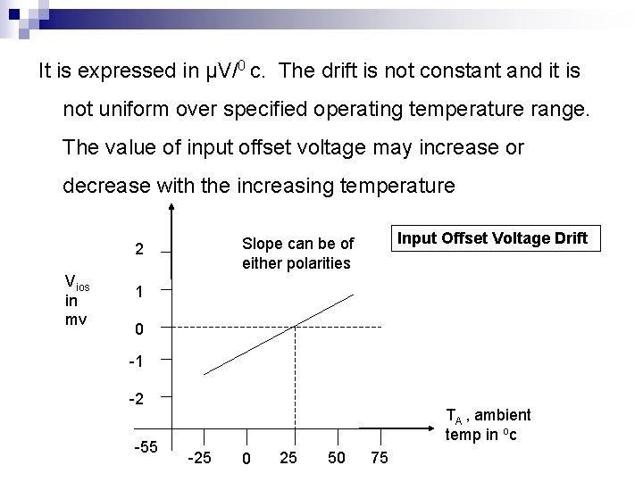
It is expressed in μV/0 c. The drift is not constant and it is not uniform over specified operating temperature range. The value of input offset voltage may increase or decrease with the increasing temperature Vios in mv Input Offset Voltage Drift Slope can be of either polarities 2 1 0 -1 -2 -55 TA , ambient temp in oc -25 0 25 50 75

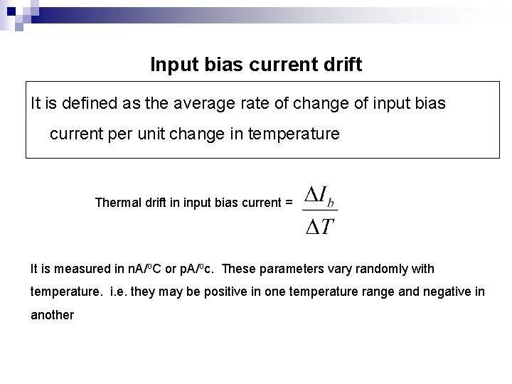
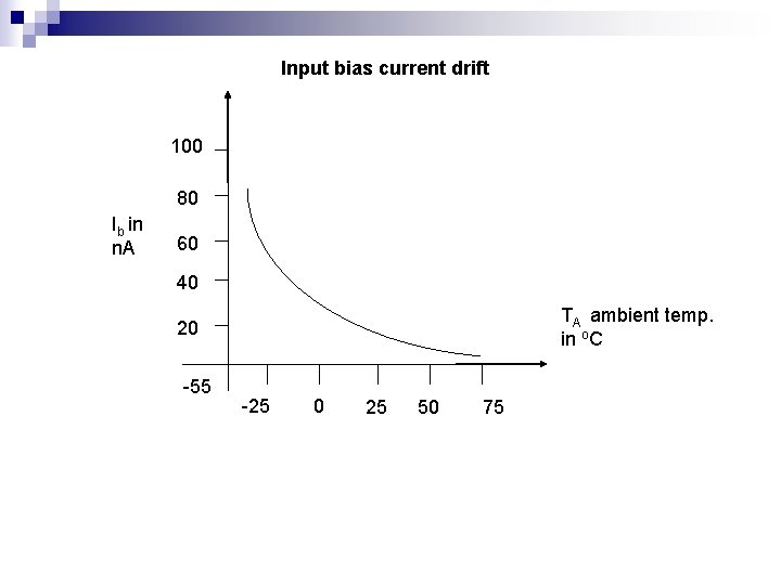
Input bias current drift It is defined as the average rate of change of input bias current per unit change in temperature Thermal drift in input bias current = It is measured in n. A/o. C or p. A/oc. These parameters vary randomly with temperature. i. e. they may be positive in one temperature range and negative in another

Input bias current drift 100 80 Ib in n. A 60 40 TA ambient temp. in o. C 20 -55 -25 0 25 50 75

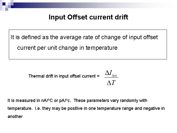
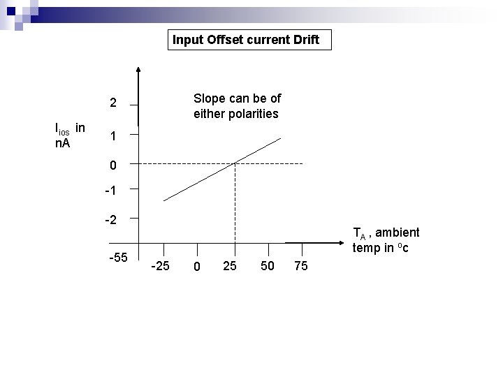
Input Offset current drift It is defined as the average rate of change of input offset current per unit change in temperature Thermal drift in input offset current = It is measured in n. A/o. C or p. A/oc. These parameters vary randomly with temperature. i. e. they may be positive in one temperature range and negative in another

Input Offset current Drift Slope can be of either polarities 2 Iios in n. A 1 0 -1 -2 -55 TA , ambient temp in oc -25 0 25 50 75

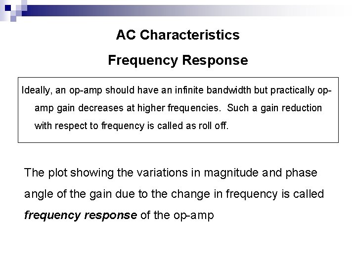
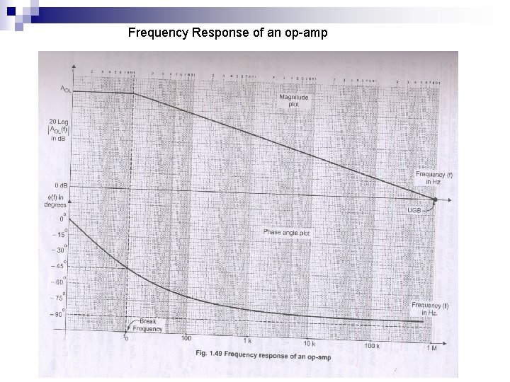
AC Characteristics Frequency Response Ideally, an op-amp should have an infinite bandwidth but practically opamp gain decreases at higher frequencies. Such a gain reduction with respect to frequency is called as roll off. The plot showing the variations in magnitude and phase angle of the gain due to the change in frequency is called frequency response of the op-amp

When the gain in decibels, phase angle in degrees are plotted against logarithmic scale of frequency, the plot is called Bode Plot The manner in which the gain of the op-amp changes with variation in frequency is known as the magnitude plot. The manner in which the phase shift changes with variation in frequency is known as the phase-angle plot.

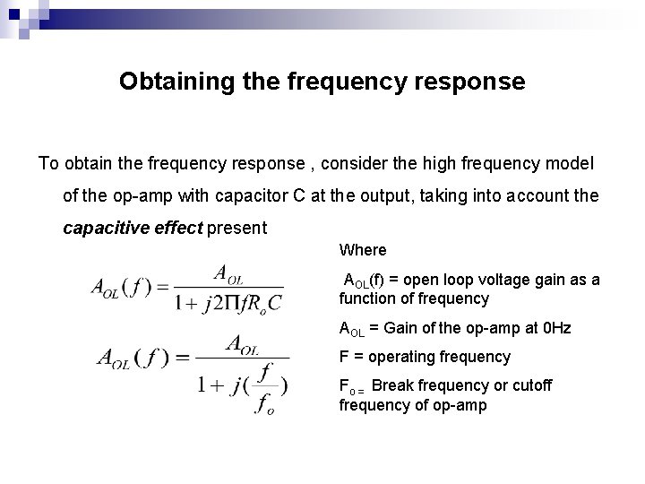
Obtaining the frequency response To obtain the frequency response , consider the high frequency model of the op-amp with capacitor C at the output, taking into account the capacitive effect present Where AOL(f) = open loop voltage gain as a function of frequency AOL = Gain of the op-amp at 0 Hz F = operating frequency Fo = Break frequency or cutoff frequency of op-amp

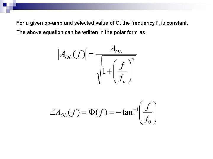
For a given op-amp and selected value of C, the frequency fo is constant. The above equation can be written in the polar form as

Frequency Response of an op-amp

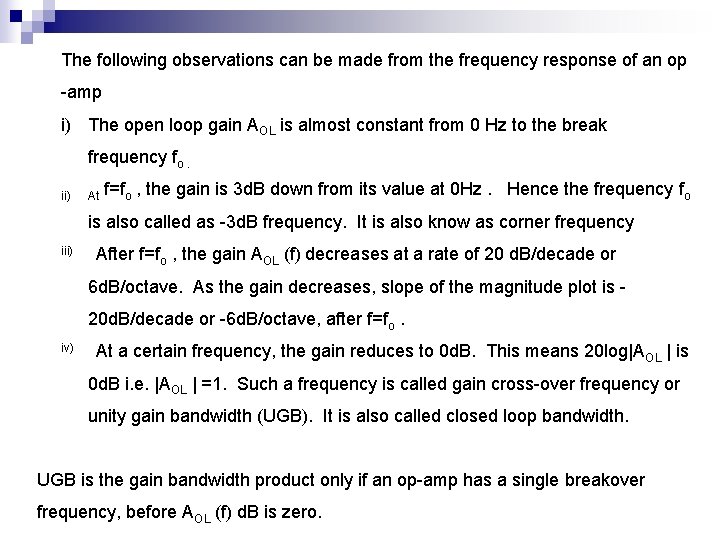
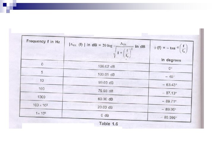
The following observations can be made from the frequency response of an op -amp i) The open loop gain AOL is almost constant from 0 Hz to the break frequency fo. ii) At f=fo , the gain is 3 d. B down from its value at 0 Hz. Hence the frequency fo is also called as -3 d. B frequency. It is also know as corner frequency iii) After f=fo , the gain AOL (f) decreases at a rate of 20 d. B/decade or 6 d. B/octave. As the gain decreases, slope of the magnitude plot is 20 d. B/decade or -6 d. B/octave, after f=fo. iv) At a certain frequency, the gain reduces to 0 d. B. This means 20 log|AOL | is 0 d. B i. e. |AOL | =1. Such a frequency is called gain cross-over frequency or unity gain bandwidth (UGB). It is also called closed loop bandwidth. UGB is the gain bandwidth product only if an op-amp has a single breakover frequency, before AOL (f) d. B is zero.

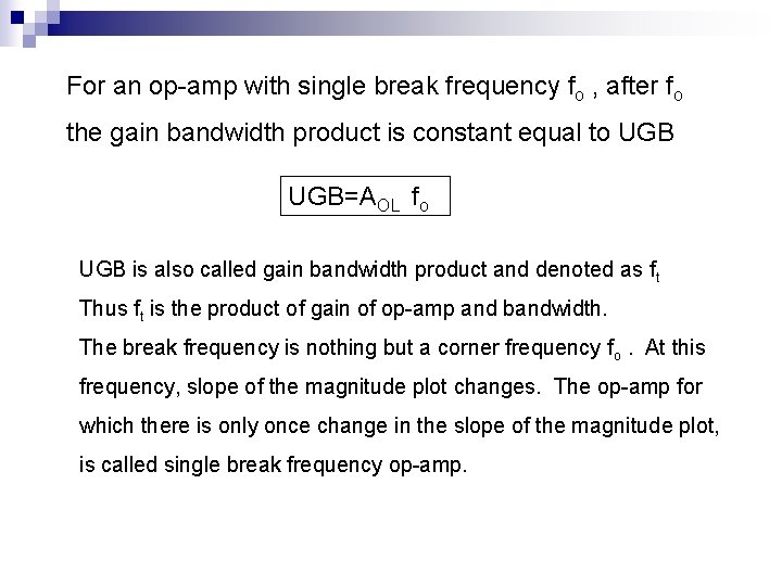
For an op-amp with single break frequency fo , after fo the gain bandwidth product is constant equal to UGB=AOL fo UGB is also called gain bandwidth product and denoted as ft Thus ft is the product of gain of op-amp and bandwidth. The break frequency is nothing but a corner frequency fo. At this frequency, slope of the magnitude plot changes. The op-amp for which there is only once change in the slope of the magnitude plot, is called single break frequency op-amp.

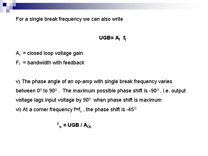
For a single break frequency we can also write UGB= Af ff Af = closed loop voltage gain Ff = bandwidth with feedback v) The phase angle of an op-amp with single break frequency varies between 00 to 900. The maximum possible phase shift is -900 , i. e. output voltage lags input voltage by 900 when phase shift is maximum vi) At a corner frequency f=fo , the phase shift is -450. F o = UGB / AOL


The modes of using an op-amp n Open Loop : (The output assumes one of the two possible output states, that is +Vsat or – Vsat and the amplifier acts as a switch only). n Closed Loop: ( The utility of an op-amp can be greatly increased by providing negative feed back. The output in this case is not driven into saturation and the circuit behaves in a linear manner).

Open loop configuration of op-amp n The voltage transfer curve indicates the inability of opamp to work as a linear small signal amplifier in the open loop mode n Such an open loop behaviour of the op-amp finds some rare applications like voltage comparator, zero crossing detector etc.

Open loop op-amp configurations n The configuration in which output depends on input, but output has no effect on the input is called open loop configuration. n No feed back from output to input is used in such configuration. n The opamp works as high gain amplifier n The op-amp can be used in three modes in open loop configuration they are 1. Differential amplifier 2. Inverting amplifier 3. Non inverting amplifier

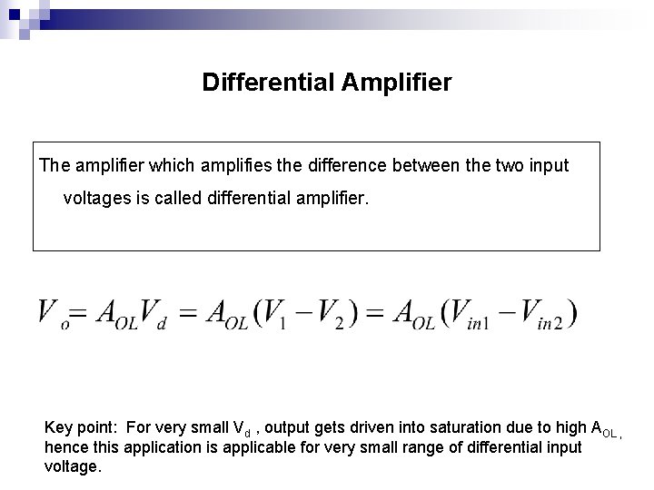
Differential Amplifier The amplifier which amplifies the difference between the two input voltages is called differential amplifier. Key point: For very small Vd , output gets driven into saturation due to high AOL , hence this application is applicable for very small range of differential input voltage.

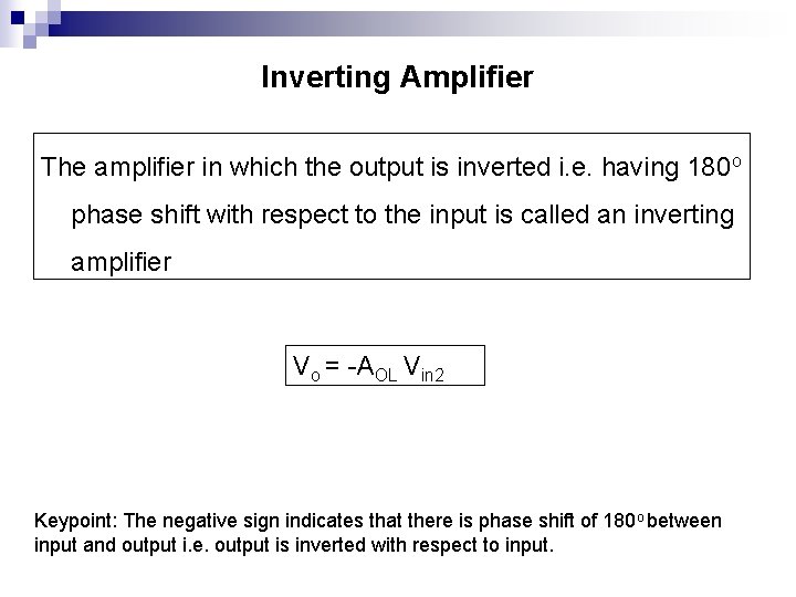
Inverting Amplifier The amplifier in which the output is inverted i. e. having 180 o phase shift with respect to the input is called an inverting amplifier Vo = -AOL Vin 2 Keypoint: The negative sign indicates that there is phase shift of 180 o between input and output i. e. output is inverted with respect to input.

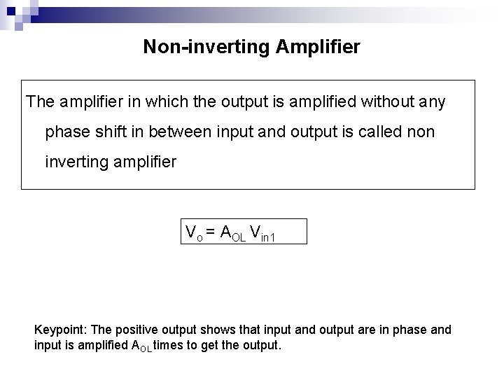
Non-inverting Amplifier The amplifier in which the output is amplified without any phase shift in between input and output is called non inverting amplifier Vo = AOL Vin 1 Keypoint: The positive output shows that input and output are in phase and input is amplified AOL times to get the output.

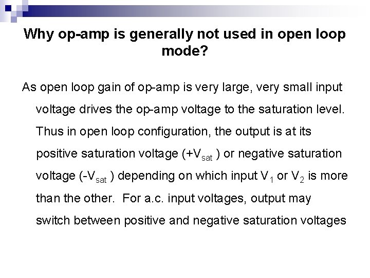
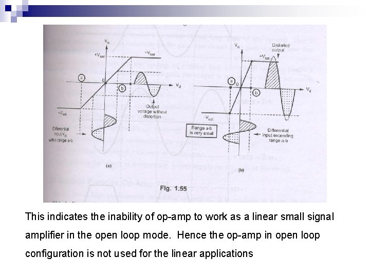
Why op-amp is generally not used in open loop mode? As open loop gain of op-amp is very large, very small input voltage drives the op-amp voltage to the saturation level. Thus in open loop configuration, the output is at its positive saturation voltage (+Vsat ) or negative saturation voltage (-Vsat ) depending on which input V 1 or V 2 is more than the other. For a. c. input voltages, output may switch between positive and negative saturation voltages

This indicates the inability of op-amp to work as a linear small signal amplifier in the open loop mode. Hence the op-amp in open loop configuration is not used for the linear applications

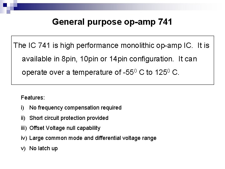
General purpose op-amp 741 The IC 741 is high performance monolithic op-amp IC. It is available in 8 pin, 10 pin or 14 pin configuration. It can operate over a temperature of -550 C to 1250 C. Features: i) No frequency compensation required ii) Short circuit protection provided iii) Offset Voltage null capability iv) Large common mode and differential voltage range v) No latch up

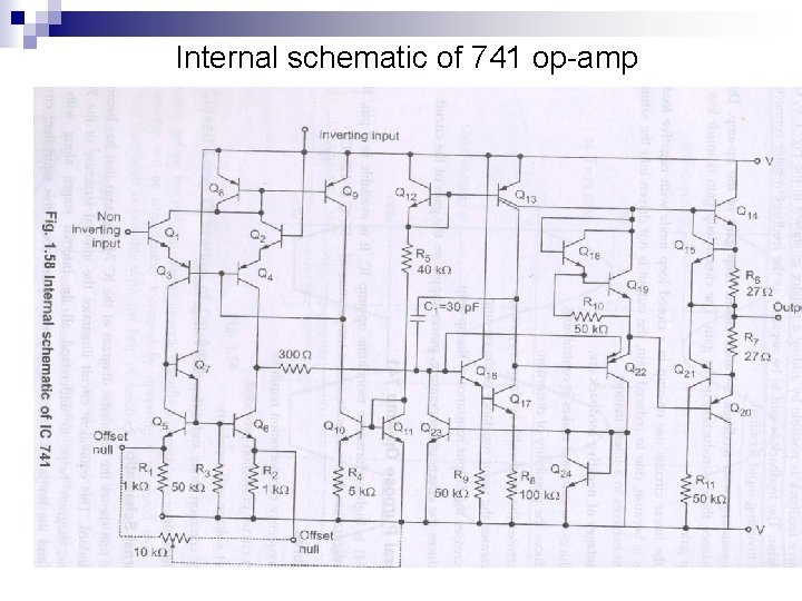
Internal schematic of 741 op-amp

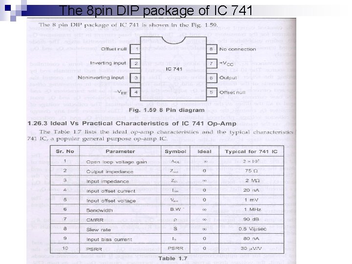
The 8 pin DIP package of IC 741

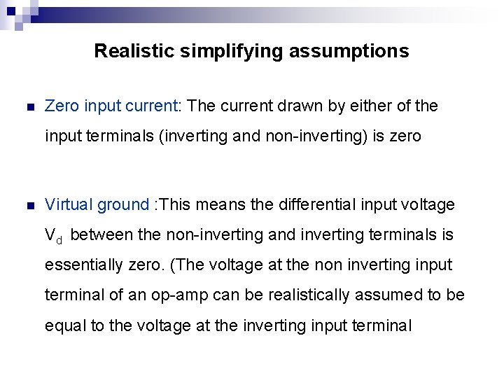
Realistic simplifying assumptions n Zero input current: The current drawn by either of the input terminals (inverting and non-inverting) is zero n Virtual ground : This means the differential input voltage Vd between the non-inverting and inverting terminals is essentially zero. (The voltage at the non inverting input terminal of an op-amp can be realistically assumed to be equal to the voltage at the inverting input terminal

Closed loop operation of op-amp The utility of the op-amp can be increased considerably by operating in closed loop mode. The closed loop operation is possible with the help of feedback. The feedback allows to feed some part of the output back to the input terminals. In the linear applications, the opamp is always used with negative feedback. The negative feedback helps in controlling gain, which otherwise drives the op-amp out of its linear range, even for a small noise voltage at the input terminals

Ideal Inverting Amplifier 1. The output is inverted with respect to input, which is indicated by minus sign. 2. The voltage gain is independent of open loop gain of the op-amp, which is assumed to be large. 3. The voltage gain depends on the ratio of the two resistances. Hence selecting Rf and R 1 , the required value of gain can be easily obtained. 4. If Rf > R 1, , the gain is greater than 1 If Rf < R 1, , the gain is less than 1 If Rf = R 1, the gain is unity Thus the output voltage can be greater than, less than or equal to the input voltage in magnitude

5. If the ratio of Rf and R 1 is K which is other than one, the circuit is called scale changer while for Rf/R 1 =1 it is called phase inverter. 6. The closed loop gain is denoted as AVF or ACL i. e. gain with feedback

Ideal Non-inverting Amplifier 1. The voltage gain is always greater than one 2. The voltage gain is positive indicating that for a. c. input, the output and input are in phase while for d. c. input, the output polarity is same as that of input 3. The voltage gain is independent of open loop gain of op-amp, but depends only on the two resistance values 4. The desired voltage gain can be obtained by selecting proper values of Rf and R 1

Comparison of the ideal inverting and noninverting op-amp Ideal Inverting amplifier Ideal non-inverting amplifier 1. Voltage gain=-Rf/R 1 1. Voltage gain=1+Rf/R 1 2. The output is inverted with 2. No phase shift between input respect to input and output 3. The voltage gain can be 3. The voltage gain is always adjusted as greater than, equal to greater than one or less than one 4. The input impedance is R 1 4. The input impedance is very large

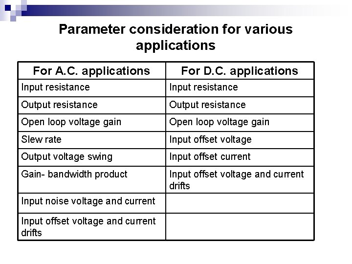
Parameter consideration for various applications For A. C. applications For D. C. applications Input resistance Output resistance Open loop voltage gain Slew rate Input offset voltage Output voltage swing Input offset current Gain- bandwidth product Input offset voltage and current drifts Input noise voltage and current Input offset voltage and current drifts

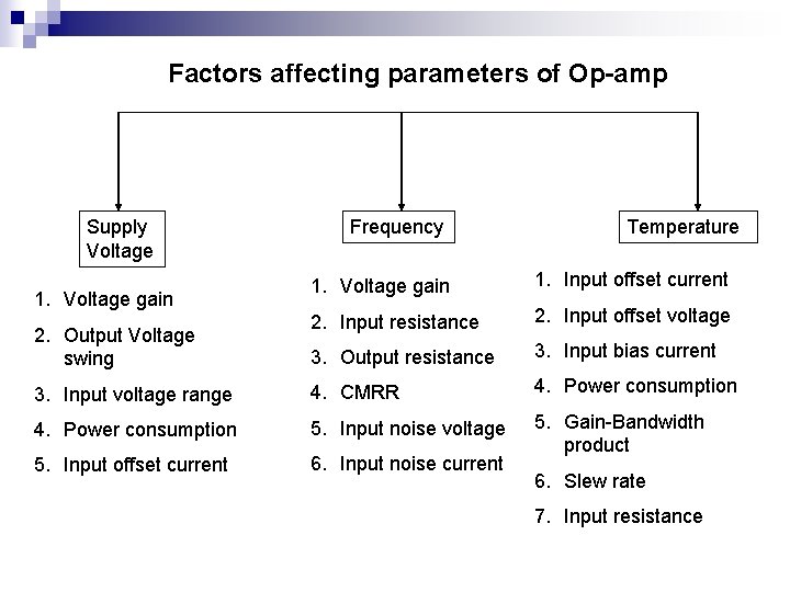
Factors affecting parameters of Op-amp Supply Voltage Frequency Temperature 1. Voltage gain 1. Input offset current 2. Input resistance 2. Input offset voltage 3. Output resistance 3. Input bias current 3. Input voltage range 4. CMRR 4. Power consumption 5. Input noise voltage 5. Input offset current 6. Input noise current 5. Gain-Bandwidth product 1. Voltage gain 2. Output Voltage swing 6. Slew rate 7. Input resistance

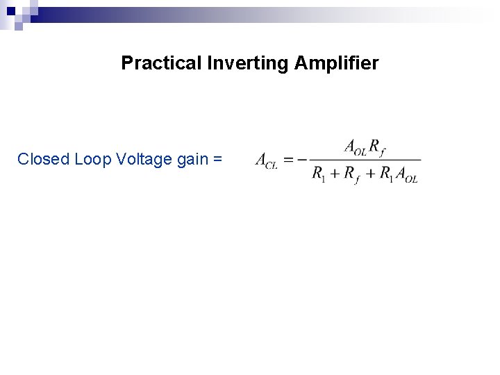
Practical Inverting Amplifier Closed Loop Voltage gain =

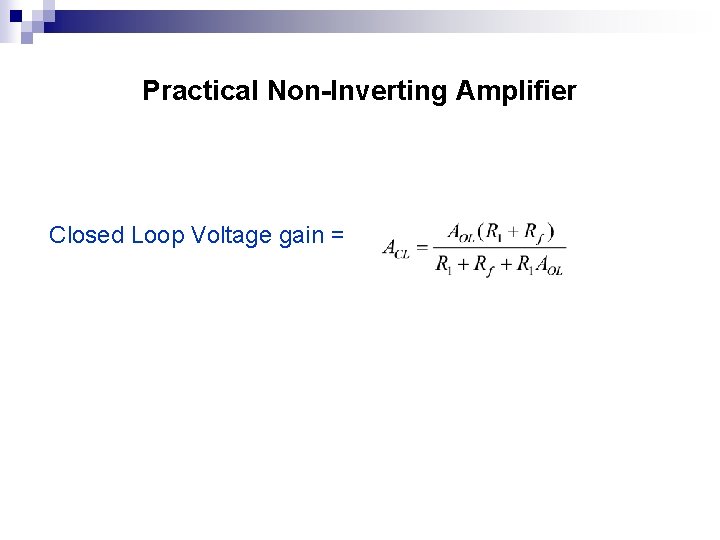
Practical Non-Inverting Amplifier Closed Loop Voltage gain =

The End