EE 174 Fall 2017 Operational Amplifiers Contents Introduction


- Slides: 27

EE 174 Fall 2017 Operational Amplifiers

Contents • Introduction • Brief of History • Fundamentals of Op-Amps • Basic operation • Gain • Offset • Applications

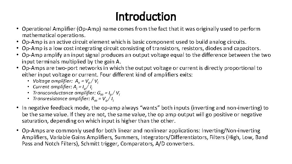
Introduction • Operational Amplifier (Op-Amp) name comes from the fact that it was originally used to perform mathematical operations. • Op-Amp is an active circuit element which is basic component used to build analog circuits. • Op-Amp is a low cost integrating circuit consisting of transistors, resistors, diodes and capacitors. • Op-Amp amplify an input signal produces an output voltage equal to the difference between the two input terminals multiplied by the gain A. • Op-Amps are two-port networks in which the output voltage or current is directly proportional to either input voltage or current. Four different kind of amplifiers exits: • • Voltage amplifier: Av = Vo / Vi Current amplifier: Ai = Io / Ii Transconductance amplifier: Gm = Io / Vi Transresistance amplifier: Rm = Vo / Ii • In negative feedback mode, the op-amp always “wants” both inputs (inverting and non-inverting) to be the same value. If they are not, the same value, the op amp output will go positive or negative saturation, depending on which input is higher than the other. • Op-Amps are commonly used for both linear and nonlinear applications: Inverting/Non-inverting Amplifiers, Variable Gains Amplifiers, Summers, Integrators/Differentiators, Filters (High, Low, Band Pass and Notch Filters), Schmitt trigger, Comparators, A/D converters.

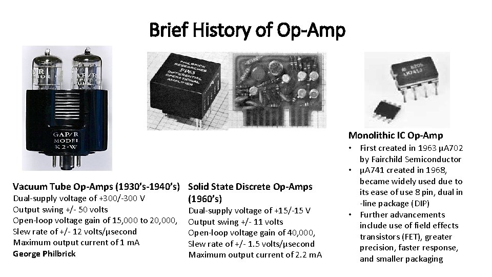
Brief History of Op-Amp Monolithic IC Op-Amp Vacuum Tube Op-Amps (1930’s-1940’s) Solid State Discrete Op-Amps Dual-supply voltage of +300/-300 V (1960’s) Output swing +/- 50 volts Open-loop voltage gain of 15, 000 to 20, 000, Slew rate of +/- 12 volts/µsecond Maximum output current of 1 m. A George Philbrick Dual-supply voltage of +15/-15 V Output swing +/- 11 volts Open-loop voltage gain of 40, 000, Slew rate of +/- 1. 5 volts/µsecond Maximum output current of 2. 2 m. A • First created in 1963 μA 702 by Fairchild Semiconductor • μA 741 created in 1968, became widely used due to its ease of use 8 pin, dual in -line package (DIP) • Further advancements include use of field effects transistors (FET), greater precision, faster response, and smaller packaging

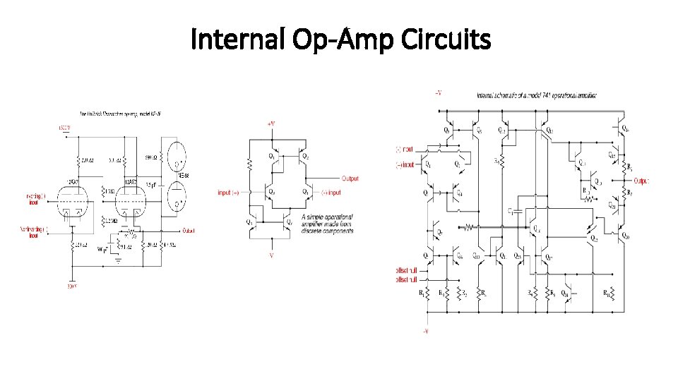
Internal Op-Amp Circuits

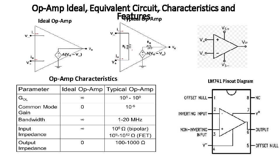
Op-Amp Ideal, Equivalent Circuit, Characteristics and Features Typical Op-Amp Ideal Op-Amp Characteristics

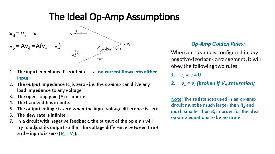
The Ideal Op-Amp Assumptions vd = v+ – vvo = Avd = A(v+ – v-) 1. The input impedance Ri is infinite - i. e. no current flows into either input. 2. The output impedance Ro is zero - i. e. the op-amp can drive any load impedance to any voltage. 3. The open-loop gain (A) is infinite. 4. The bandwidth is infinite. 5. The output voltage is zero when the input voltage difference is zero. 6. The slew rate is infinite 7. In a circuit with negative feedback, the output of the op amp will try to adjust its output so that the voltage difference between the + and − inputs is zero (V+ = V−). Op-Amp Golden Rules: When an op-amp is configured in any negative-feedback arrangement, it will obey the following two rules: 1. i+ = i-= 0 2. v+ = v- (broken if VO saturation) Note: The resistances used in an op-amp circuit must be much larger than Ro and much smaller than Ri in order for the ideal op-amp equations to be accurate.

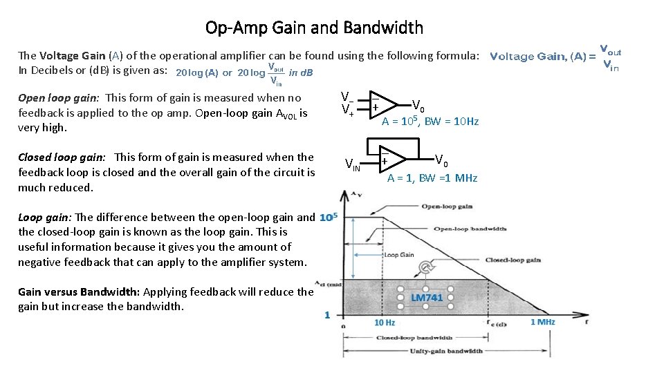
Op-Amp Gain and Bandwidth The Voltage Gain (A) of the operational amplifier can be found using the following formula: In Decibels or (d. B) is given as: Closed loop gain: This form of gain is measured when the feedback loop is closed and the overall gain of the circuit is much reduced. VIN Loop gain: The difference between the open-loop gain and the closed-loop gain is known as the loop gain. This is useful information because it gives you the amount of negative feedback that can apply to the amplifier system. Gain versus Bandwidth: Applying feedback will reduce the gain but increase the bandwidth. V 0 A = 105, BW = 10 Hz + V V+ + Open loop gain: This form of gain is measured when no feedback is applied to the op amp. Open-loop gain AVOL is very high. V 0 A = 1, BW =1 MHz

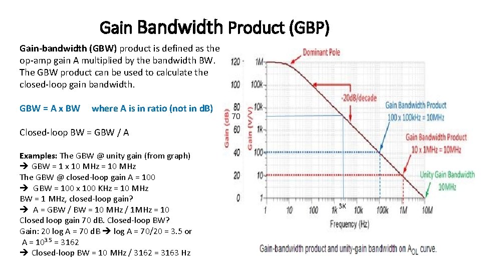
Gain Bandwidth Product (GBP) Gain-bandwidth (GBW) product is defined as the op-amp gain A multiplied by the bandwidth BW. The GBW product can be used to calculate the closed-loop gain bandwidth. GBW = A x BW where A is in ratio (not in d. B) Closed-loop BW = GBW / A Examples: The GBW @ unity gain (from graph) GBW = 1 x 10 MHz = 10 MHz The GBW @ closed-loop gain A = 100 GBW = 100 x 100 KHz = 10 MHz BW = 1 MHz, closed-loop gain? A = GBW / BW = 10 MHz / 1 MHz = 10 Closed loop gain 70 d. B. Closed-loop BW? Gain: 20 log A = 70 d. B log A = 70/20 = 3. 5 or A = 103. 5 = 3162 Closed-loop BW = 10 MHz / 3162 = 3163 Hz

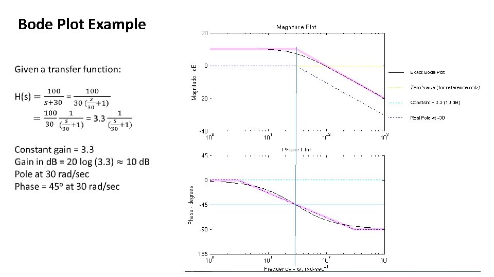
Bode Plot Example

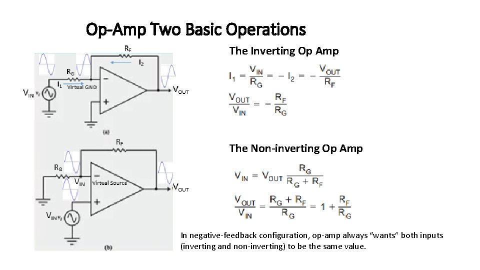
Op-Amp Two Basic Operations The Inverting Op Amp The Non-inverting Op Amp In negative-feedback configuration, op-amp always “wants” both inputs (inverting and non-inverting) to be the same value.

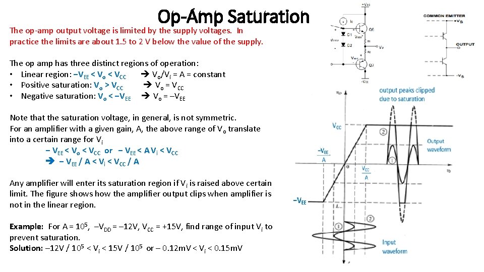
Op-Amp Saturation The op-amp output voltage is limited by the supply voltages. In practice the limits are about 1. 5 to 2 V below the value of the supply. The op amp has three distinct regions of operation: • Linear region: −VEE < Vo < VCC Vo/Vi = A = constant • Positive saturation: Vo > VCC Vo = VCC • Negative saturation: Vo < −VEE Vo = –VEE Note that the saturation voltage, in general, is not symmetric. For an amplifier with a given gain, A, the above range of Vo translate into a certain range for Vi − VEE < Vo < VCC or − VEE < A Vi < VCC − VEE / A < Vi < VCC / A Any amplifier will enter its saturation region if Vi is raised above certain limit. The figure shows how the amplifier output clips when amplifier is not in the linear region. Example: For A = 105, –VDD = – 12 V, VCC = +15 V, find range of input Vi to prevent saturation. Solution: – 12 V / 105 < Vi < 15 V / 105 or – 0. 12 m. V < Vi < 0. 15 m. V

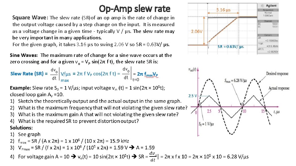
Op-Amp slew rate Square Wave: The slew rate (SR)of an op amp is the rate of change in the output voltage caused by a step change on the input. It is measured as a voltage change in a given time - typically V / µs. The slew rate may be very important in many applications. For the given graph, it takes 3. 16 µs to swing 2. 06 V so SR = 0. 63 V/ µs. Sine Waves: The maximum rate of change for a sine wave occurs at the zero crossing and for a given vo = VP sin(2π f t), the slew rate SR is: SR = 0. 63 V/ µs.

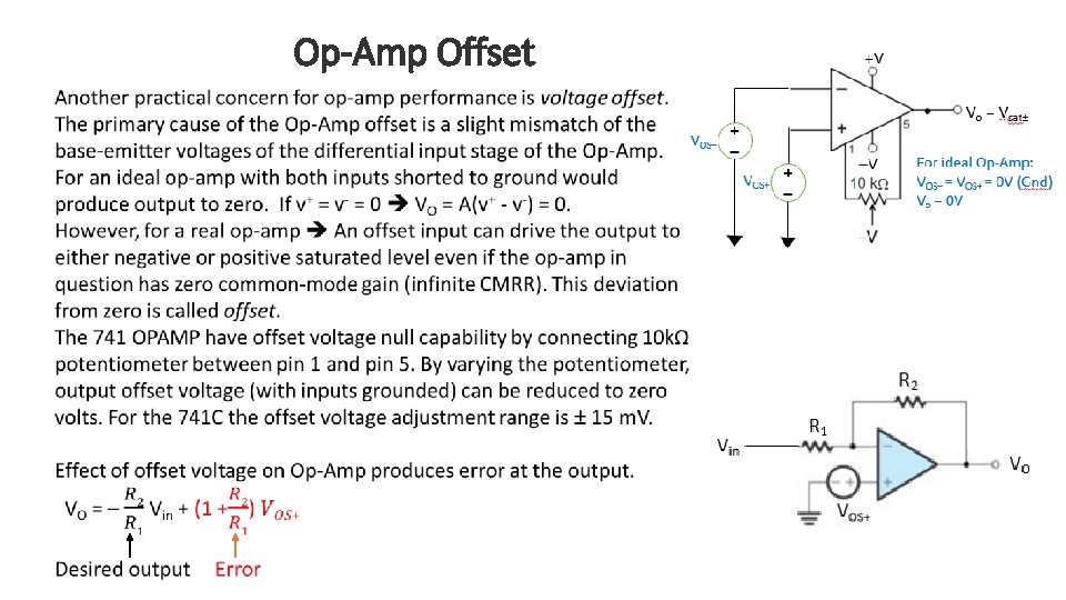
Op-Amp Offset

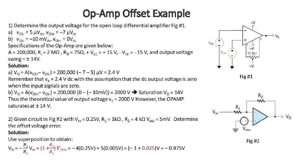
Op-Amp Offset Example Fig #1 Fig #2

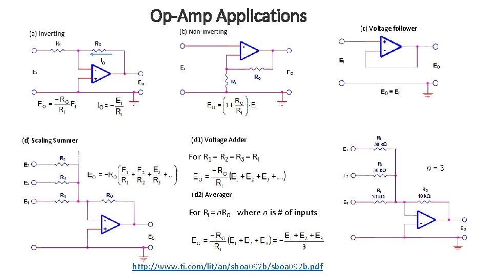
Op-Amp Applications (c) Voltage follower IO (d) Scaling Summer (d 1) Voltage Adder n = 3 (d 2) Averager For RI = n. RO where n is # of inputs http: //www. ti. com/lit/an/sboa 092 b. pdf

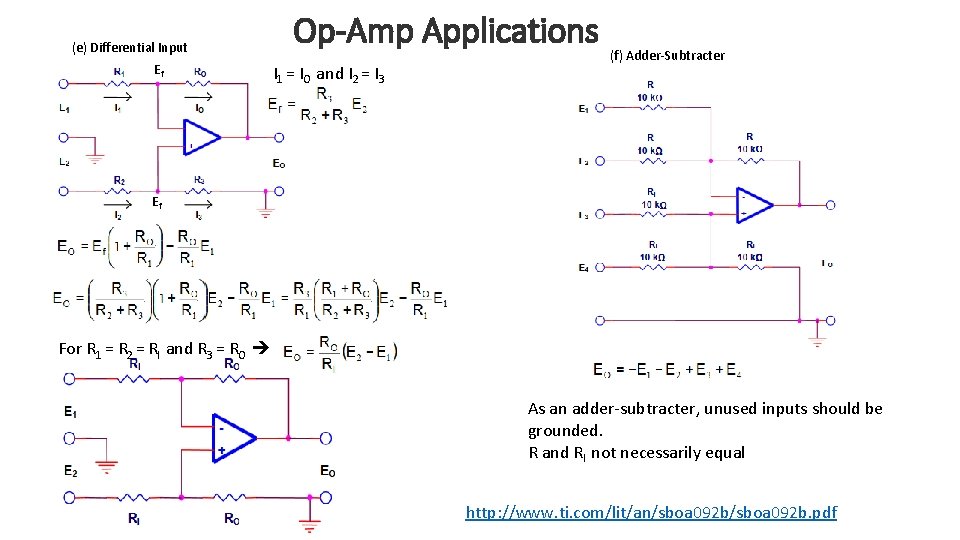
(e) Differential Input Ef Op-Amp Applications I 1 = IO and I 2 = I 3 (f) Adder-Subtracter Ef For R 1 = R 2 = RI and R 3 = RO As an adder-subtracter, unused inputs should be grounded. R and RI not necessarily equal http: //www. ti. com/lit/an/sboa 092 b. pdf

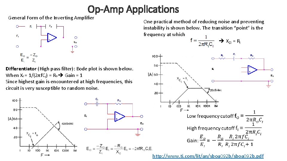
Op-Amp Applications General Form of the Inverting Amplifier One practical method of reducing noise and preventing instability is shown below. The transition “point” is the frequency at which XCI = RI Differentiator (High pass filter): Bode plot is shown below. When XC = 1/(2πf. CI) = RO Gain = 1 Since highest gain is encountered at high frequencies, this circuit is very susceptible to random noise. http: //www. ti. com/lit/an/sboa 092 b. pdf

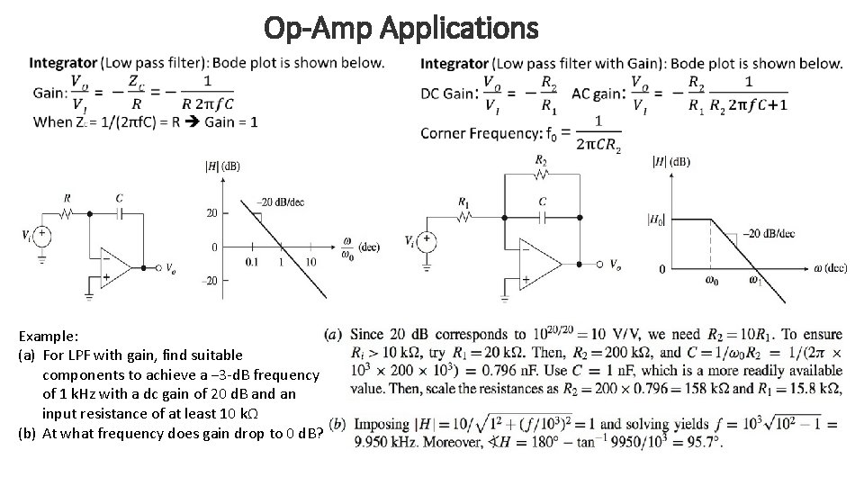
Op-Amp Applications Example: (a) For LPF with gain, find suitable components to achieve a − 3 -d. B frequency of 1 k. Hz with a dc gain of 20 d. B and an input resistance of at least 10 kΩ (b) At what frequency does gain drop to 0 d. B?

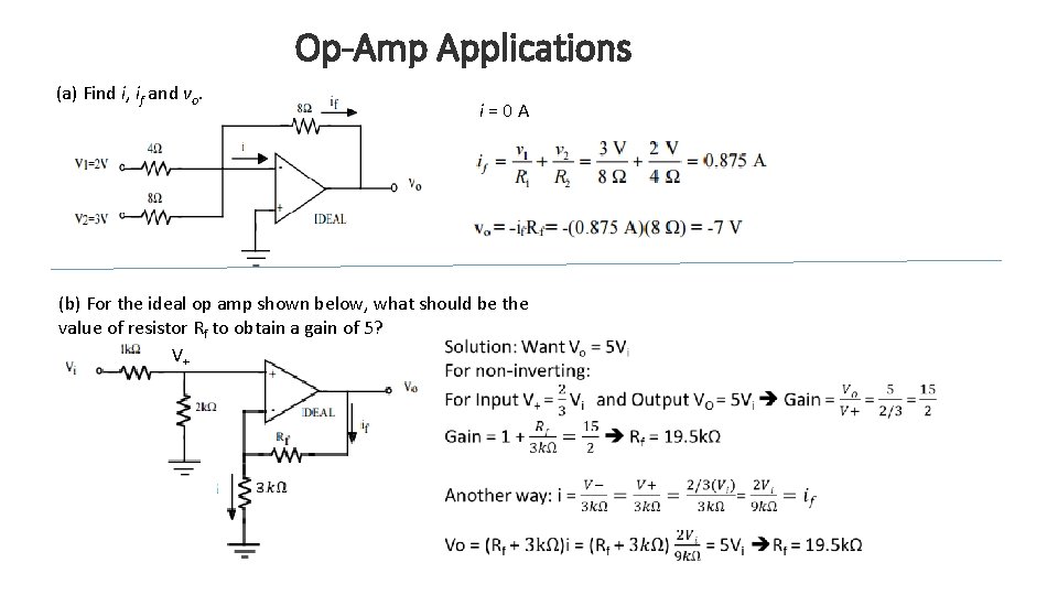
Op-Amp Applications (a) Find i, if and vo. i = 0 A (b) For the ideal op amp shown below, what should be the value of resistor Rf to obtain a gain of 5? V+

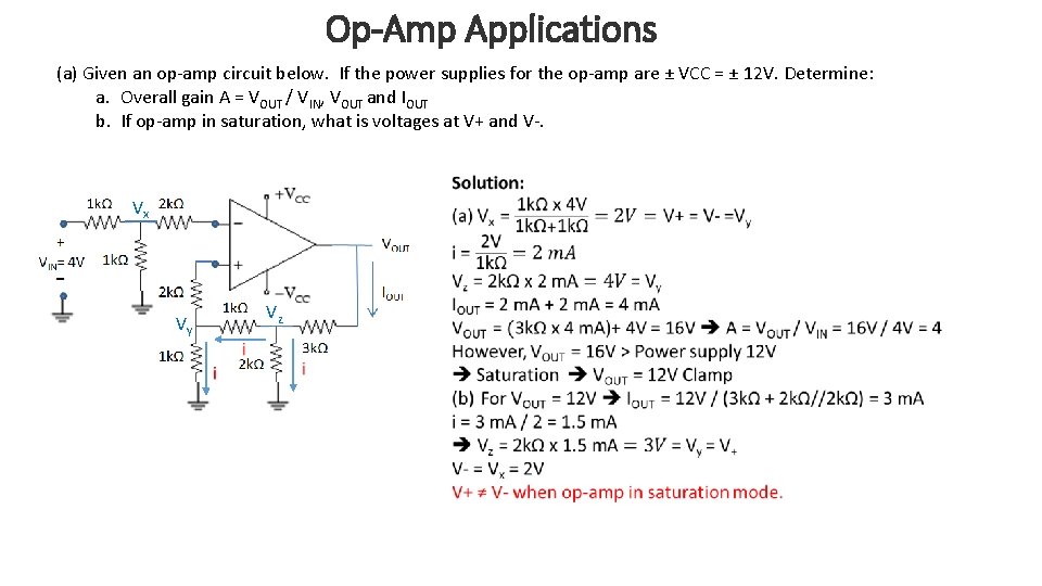
Op-Amp Applications (a) Given an op-amp circuit below. If the power supplies for the op-amp are ± VCC = ± 12 V. Determine: a. Overall gain A = VOUT / VIN, VOUT and IOUT b. If op-amp in saturation, what is voltages at V+ and V-. Vx Vz Vy

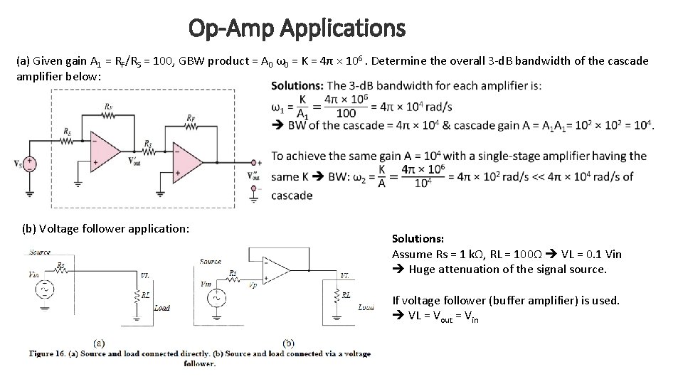
Op-Amp Applications (a) Given gain A 1 = RF/RS = 100, GBW product = A 0 ω0 = K = 4π × 106. Determine the overall 3 -d. B bandwidth of the cascade amplifier below: (b) Voltage follower application: Solutions: Assume Rs = 1 kΩ, RL = 100Ω VL = 0. 1 Vin Huge attenuation of the signal source. If voltage follower (buffer amplifier) is used. VL = Vout = Vin

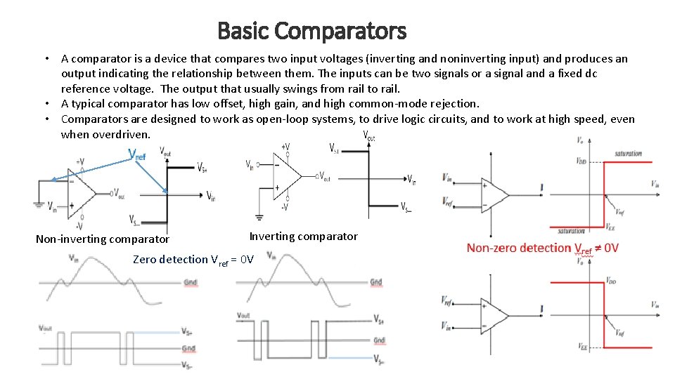
Basic Comparators • A comparator is a device that compares two input voltages (inverting and noninverting input) and produces an output indicating the relationship between them. The inputs can be two signals or a signal and a fixed dc reference voltage. The output that usually swings from rail to rail. • A typical comparator has low offset, high gain, and high common-mode rejection. • Comparators are designed to work as open-loop systems, to drive logic circuits, and to work at high speed, even when overdriven. Non-inverting comparator Inverting comparator Zero detection Vref = 0 V

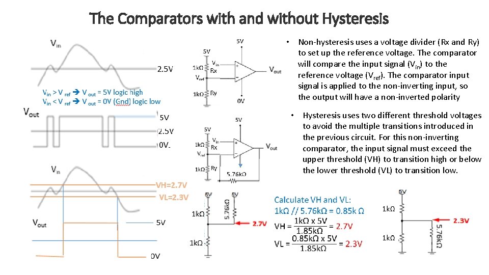
The Comparators with and without Hysteresis • Non-hysteresis uses a voltage divider (Rx and Ry) to set up the reference voltage. The comparator will compare the input signal (Vin) to the reference voltage (Vref). The comparator input signal is applied to the non-inverting input, so the output will have a non-inverted polarity • Hysteresis uses two different threshold voltages to avoid the multiple transitions introduced in the previous circuit. For this non-inverting comparator, the input signal must exceed the upper threshold (VH) to transition high or below the lower threshold (VL) to transition low.

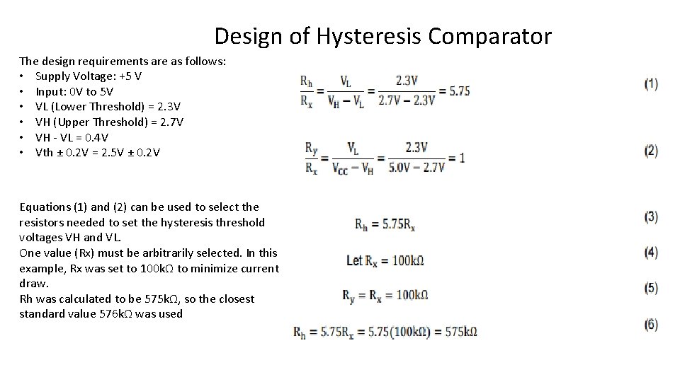
Design of Hysteresis Comparator The design requirements are as follows: • Supply Voltage: +5 V • Input: 0 V to 5 V • VL (Lower Threshold) = 2. 3 V • VH (Upper Threshold) = 2. 7 V • VH - VL = 0. 4 V • Vth ± 0. 2 V = 2. 5 V ± 0. 2 V Equations (1) and (2) can be used to select the resistors needed to set the hysteresis threshold voltages VH and VL. One value (Rx) must be arbitrarily selected. In this example, Rx was set to 100 kΩ to minimize current draw. Rh was calculated to be 575 kΩ, so the closest standard value 576 kΩ was used

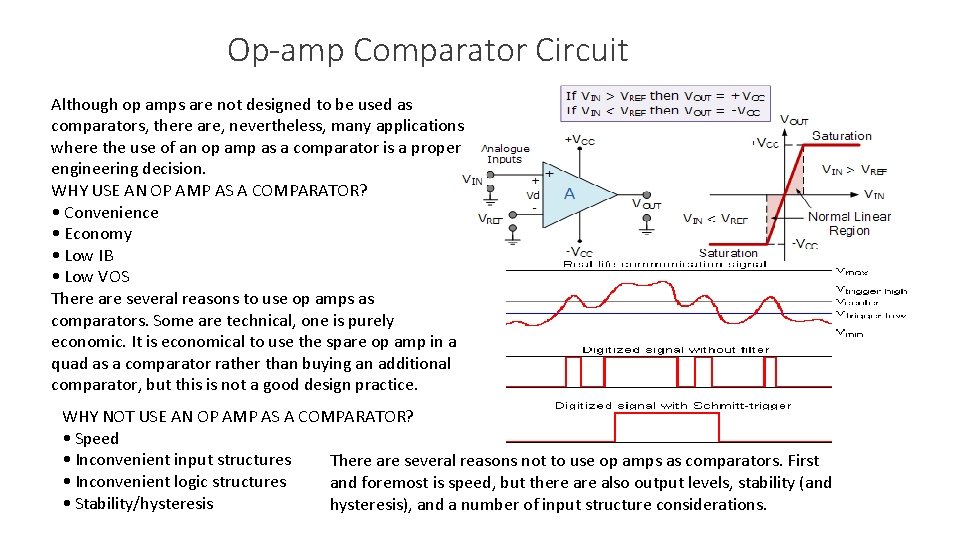
Op-amp Comparator Circuit Although op amps are not designed to be used as comparators, there are, nevertheless, many applications where the use of an op amp as a comparator is a proper engineering decision. WHY USE AN OP AMP AS A COMPARATOR? • Convenience • Economy • Low IB • Low VOS There are several reasons to use op amps as comparators. Some are technical, one is purely economic. It is economical to use the spare op amp in a quad as a comparator rather than buying an additional comparator, but this is not a good design practice. WHY NOT USE AN OP AMP AS A COMPARATOR? • Speed • Inconvenient input structures There are several reasons not to use op amps as comparators. First • Inconvenient logic structures and foremost is speed, but there also output levels, stability (and • Stability/hysteresis), and a number of input structure considerations.

References: • http: //www. ume. gatech. edu/mechatronics_course/Op. Amp_F 08. ppt • http: //www. allaboutcircuits. com/textbook/semiconductors/chpt-8/operational-amplifier-models/ • http: //www. ti. com/lit/an/slaa 068 a. pdf • http: //www. radio-electronics. com/info/circuits/opamp_basics/operational-amplifier-slew-rate. php • http: //www. planetanalog. com/author. asp? section_id=483&doc_id=562347 • http: //www-ferp. ucsd. edu/najmabadi/CLASS/ECE 60 L/02 -S/NOTES/opamp. pdf • http: //www-inst. eecs. berkeley. edu/~ee 105/fa 14/lectures/Lecture 06 -Non-ideal%20 Op%20 Amps%20(Offset-Slew%20 rate). pdf • http: //nptel. ac. in/courses/117107094//lecturers/lecture_6/lecture 6_page 1. htm • http: //www. ti. com/ww/en/bobpease/assets/AN-31. pdf • http: //www. cs. tut. fi/kurssit/TLT-8016/Chapter 2. pdf • http: //www. electronics-tutorials. ws/opamp/op-amp-comparator. html • http: //hyperphysics. phy-astr. gsu. edu/hbase/electronic/schmitt. html • http: //lpsa. swarthmore. edu/Bode. Examples. html • http: //www. allaboutcircuits. com/worksheets/inverting-and-noninverting-opamp-voltage-amplifier-circuits/ • Fundamentals of Electrical Engineering, Giorgio Rizzoni, Mc. Graw-Hill Higher Education • http: //chrisgammell. com/how-does-an-op-amp-work-part-1/ • http: //electronicdesign. com/analog/whats-all-noise-gain-stuff-anyhow • http: //howtomechatronics. com/how-it-works/electrical-engineering/schmitt-trigger/ • http: //www. analog. com/media/en/training-seminars/design-handbooks/Basic-Linear-Design/Chapter 1. pdf • http: //www. ti. com/lit/an/sloa 011. pdf • http: //www. analog. com/media/en/technical-documentation/application-notes/AN-849. pdf • http: //www. ti. com/lit/ug/tidu 020 a. pdf