Part 1 Operational Amplifier 1 1 0 Operational

- Slides: 69

Part 1 Operational Amplifier 1

1. 0 Operational Amplifier 1. 1 Introduction 1. 2 Ideal Op-Amp 1. 3 Op-amp input modes 1. 4 Op-amp Parameters 1. 5 Operation • Single-mode • Differential-mode • Common-mode operation • 1. 6 Op-Amps basics • 1. 7 Datasheet • • • 2

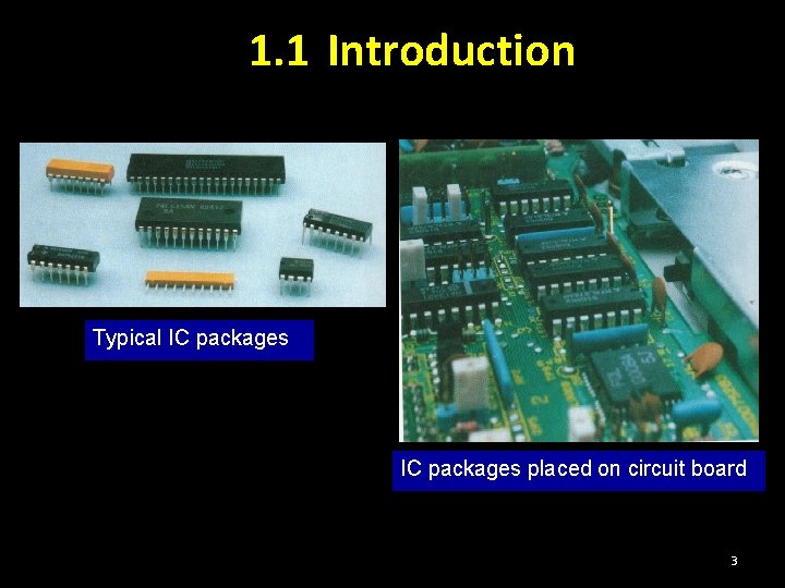
1. 1 Introduction Typical IC packages placed on circuit board 3

Uses of Op-Amp n To provide voltage amplitude changes (amplitude and polarity) n Comparators n Oscillators n Filter circuits n Instrumentation circuits 4

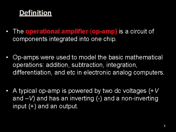
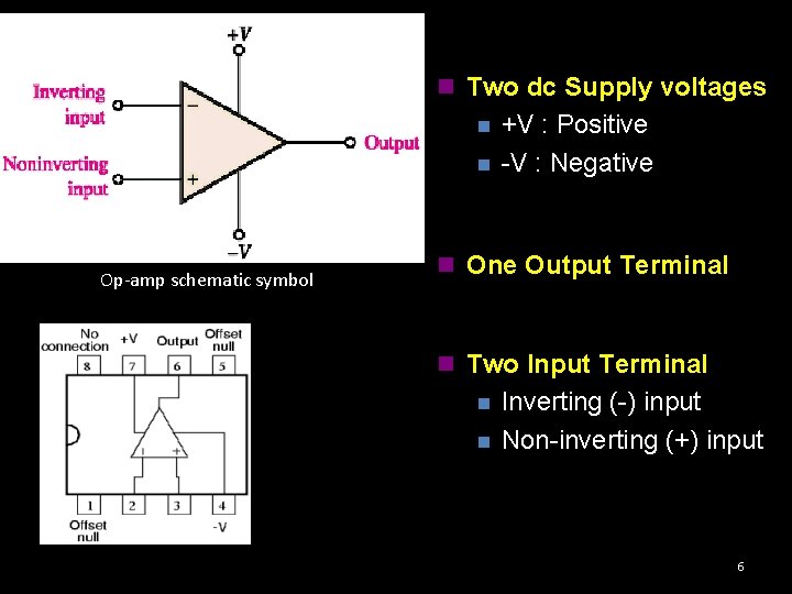
Definition • The operational amplifier (op-amp) is a circuit of components integrated into one chip. • Op-amps were used to model the basic mathematical operations: addition, subtraction, integration, differentiation, and etc in electronic analog computers. • A typical op-amp is powered by two dc voltages (+V and –V) and has an inverting (-) and a non-inverting input (+) and an output. 5

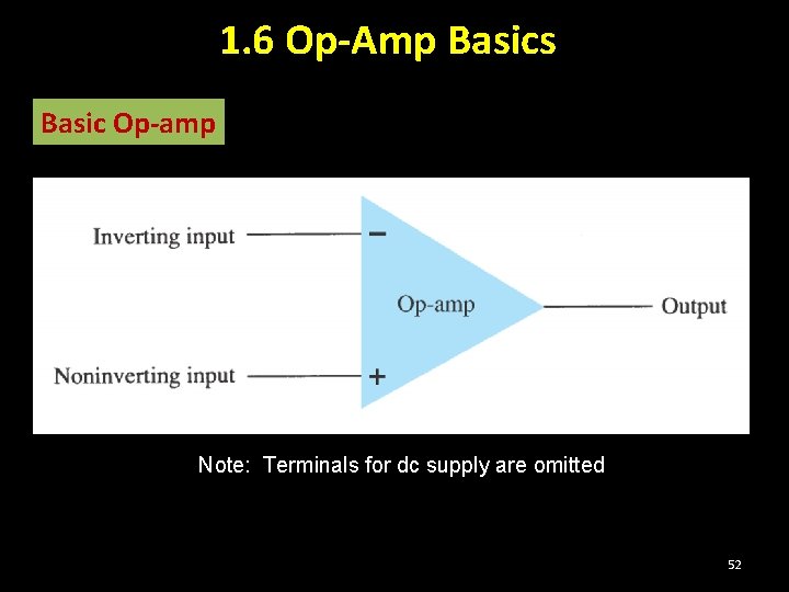
n Two dc Supply voltages n n Op-amp schematic symbol +V : Positive -V : Negative n One Output Terminal n Two Input Terminal n n Inverting (-) input Non-inverting (+) input 6

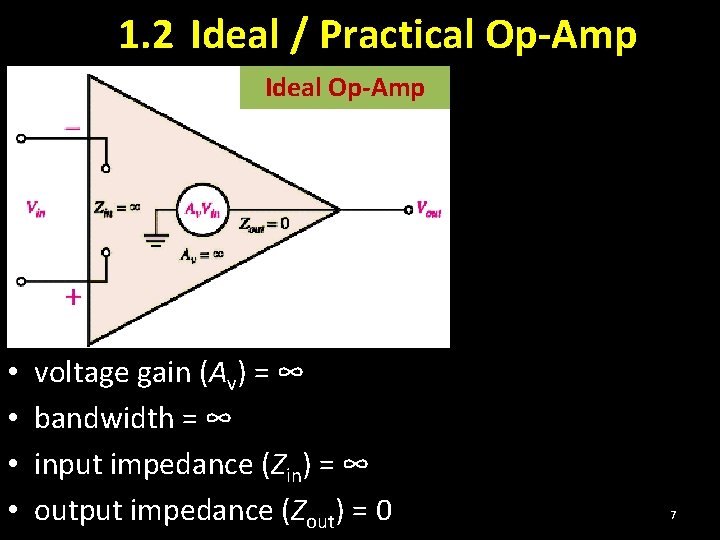
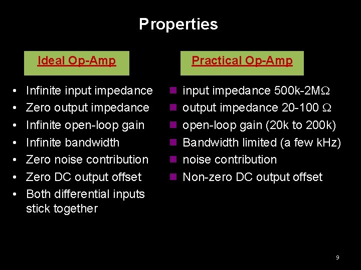
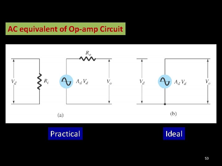
1. 2 Ideal / Practical Op-Amp Ideal Op-Amp • • voltage gain (Av) = ∞ bandwidth = ∞ input impedance (Zin) = ∞ output impedance (Zout) = 0 7

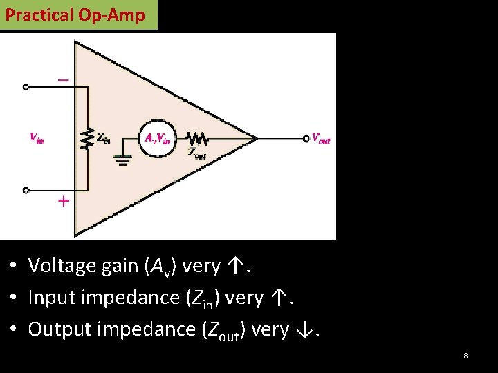
Practical Op-Amp • Voltage gain (Av) very ↑. • Input impedance (Zin) very ↑. • Output impedance (Zout) very ↓. 8

Properties Ideal Op-Amp • • Infinite input impedance Zero output impedance Infinite open-loop gain Infinite bandwidth Zero noise contribution Zero DC output offset Both differential inputs stick together Practical Op-Amp n input impedance 500 k-2 M n output impedance 20 -100 n open-loop gain (20 k to 200 k) n Bandwidth limited (a few k. Hz) n noise contribution n Non-zero DC output offset 9

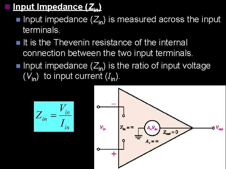
n Input Impedance (Zin) Input impedance (Zin) is measured across the input terminals. n It is the Thevenin resistance of the internal connection between the two input terminals. n Input impedance (Zin) is the ratio of input voltage (Vin) to input current (Iin). n 10

When Zin = ∞, the input current (Iin) = 0. n So, any current will neither flowing from the source supply into the amplifiers input circuitry, nor will accept current from any external circuit. n In real, the resistance is 500 k to 2 M. n 11

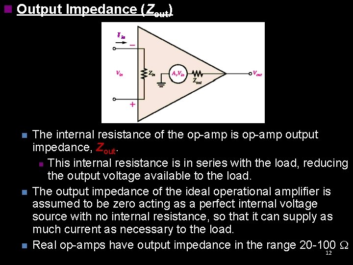
n Output Impedance (Zout) n n n The internal resistance of the op-amp is op-amp output impedance, Zout. n This internal resistance is in series with the load, reducing the output voltage available to the load. The output impedance of the ideal operational amplifier is assumed to be zero acting as a perfect internal voltage source with no internal resistance, so that it can supply as much current as necessary to the load. Real op-amps have output impedance in the range 20 -100 . 12

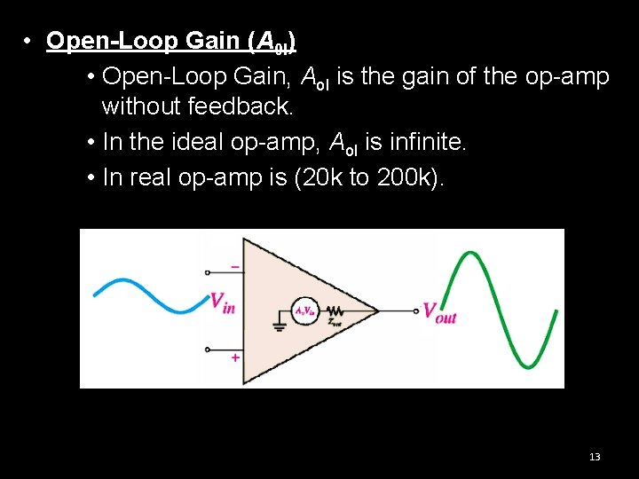
• Open-Loop Gain (A 0 l) • Open-Loop Gain, Aol is the gain of the op-amp without feedback. • In the ideal op-amp, Aol is infinite. • In real op-amp is (20 k to 200 k). 13

n Bandwidth (BW) n The ideal op-amp will amplify all signals from DC to the highest AC frequencies. n In real op-amps, the bandwidth is rather limited. n n This limitation is specified by the Gain. Bandwidth product, which is equal to the frequency where the amplifier gain becomes unity. Some op-amps, such as 741 family, have very limited bandwidth up to a few k. Hz. 14

n Noise Contribution n In an ideal op amp, all noise voltages produced are external to the op-amp. n Thus any noise in the output signal must have been in the input signal as well. n The ideal op amp contributes nothing extra to the output noise. 15

n Output Offset Voltage n The output offset voltage of any amplifier is the output voltage that exists when it should be zero. n The voltage amplifier sees zero input voltage when both inputs are grounded. This connection should produce a zero output voltage. n If the output is not zero then there is said to be an output voltage present. n In the ideal op amp this offset voltage is zero volts. n In practical op amps the output offset voltage is nonzero. 16

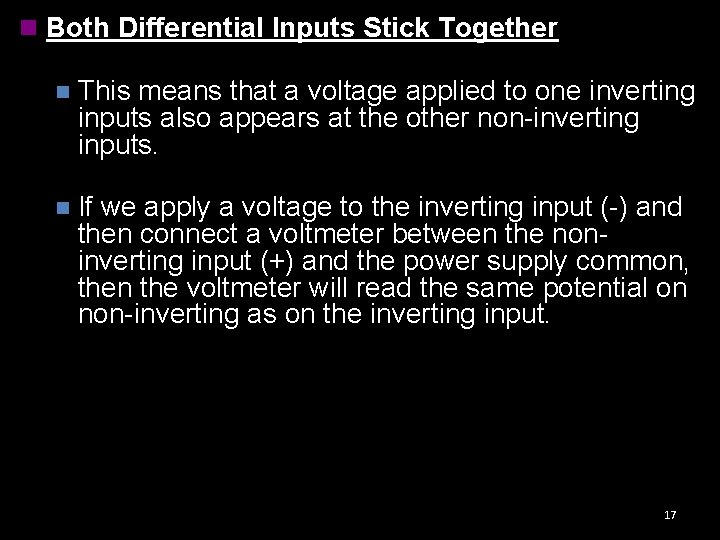
n Both Differential Inputs Stick Together n This means that a voltage applied to one inverting inputs also appears at the other non-inverting inputs. n If we apply a voltage to the inverting input (-) and then connect a voltmeter between the noninverting input (+) and the power supply common, then the voltmeter will read the same potential on non-inverting as on the inverting input. 17

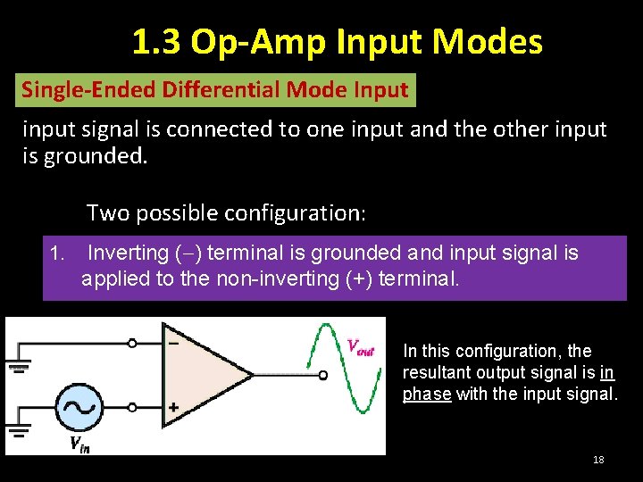
1. 3 Op-Amp Input Modes Single-Ended Differential Mode Input input signal is connected to one input and the other input is grounded. Two possible configuration: 1. Inverting ( ) terminal is grounded and input signal is applied to the non-inverting (+) terminal. In this configuration, the resultant output signal is in phase with the input signal. 18

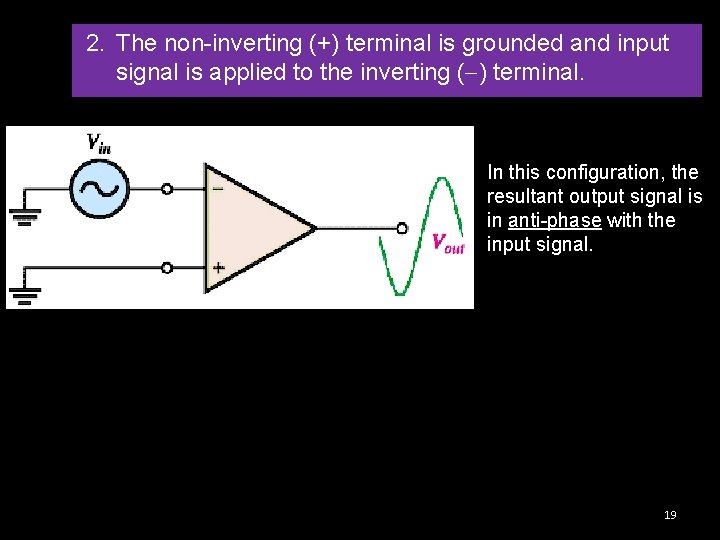
2. The non-inverting (+) terminal is grounded and input signal is applied to the inverting ( ) terminal. In this configuration, the resultant output signal is in anti-phase with the input signal. 19

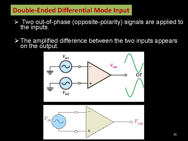
Double-Ended Differential Mode Input Ø Two out-of-phase (opposite-polarity) signals are applied to the inputs. Ø The amplified difference between the two inputs appears on the output. 20

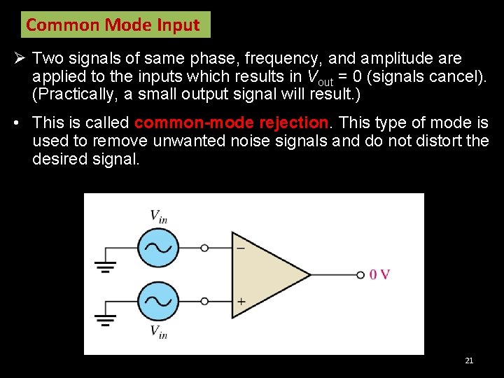
Common Mode Input Ø Two signals of same phase, frequency, and amplitude are applied to the inputs which results in Vout = 0 (signals cancel). (Practically, a small output signal will result. ) • This is called common-mode rejection. This type of mode is used to remove unwanted noise signals and do not distort the desired signal. 21

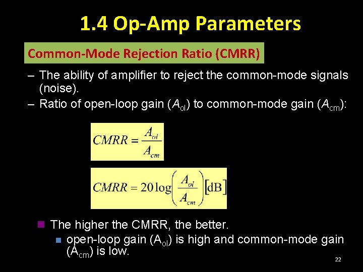
1. 4 Op-Amp Parameters Common-Mode Rejection Ratio (CMRR) – The ability of amplifier to reject the common-mode signals (noise). – Ratio of open-loop gain (Aol) to common-mode gain (Acm): n The higher the CMRR, the better. n open-loop gain (Aol) is high and common-mode gain (Acm) is low. 22

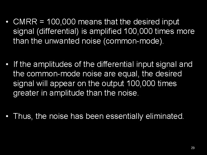
• CMRR = 100, 000 means that the desired input signal (differential) is amplified 100, 000 times more than the unwanted noise (common-mode). • If the amplitudes of the differential input signal and the common-mode noise are equal, the desired signal will appear on the output 100, 000 times greater in amplitude than the noise. • Thus, the noise has been essentially eliminated. 23

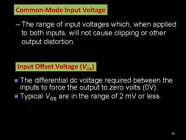
Common-Mode Input Voltage – The range of input voltages which, when applied to both inputs, will not cause clipping or other output distortion. Input Offset Voltage (VOS) The differential dc voltage required between the inputs to force the output to zero volts (0 V). n Typical VOS are in the range of 2 m. V or less. n 24

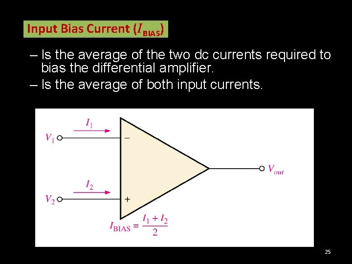
Input Bias Current (IBIAS) – Is the average of the two dc currents required to bias the differential amplifier. – Is the average of both input currents. 25

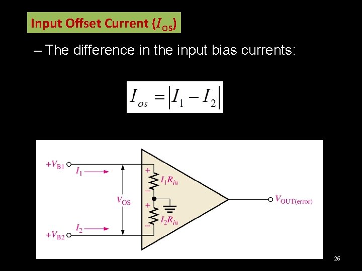
Input Offset Current (IOS) – The difference in the input bias currents: 26

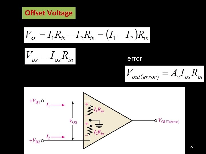
Offset Voltage error 27

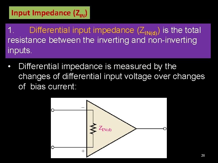
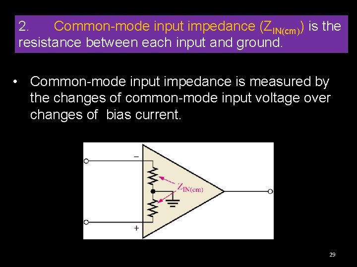
Input Impedance (ZIN) 1. Differential input impedance (ZIN(d)) is the total resistance between the inverting and non-inverting inputs. • Differential impedance is measured by the changes of differential input voltage over changes of bias current: 28

2. Common-mode input impedance (ZIN(cm)) is the resistance between each input and ground. • Common-mode input impedance is measured by the changes of common-mode input voltage over changes of bias current. 29

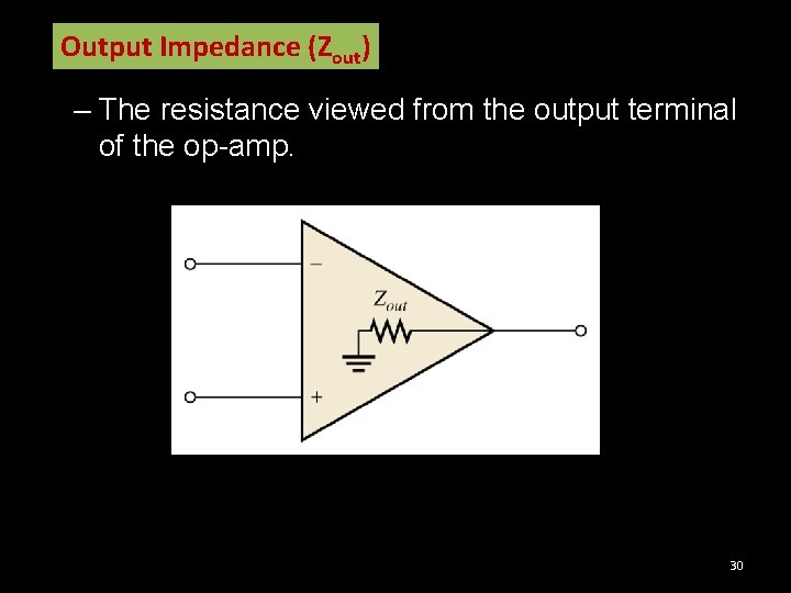
Output Impedance (Zout) – The resistance viewed from the output terminal of the op-amp. 30

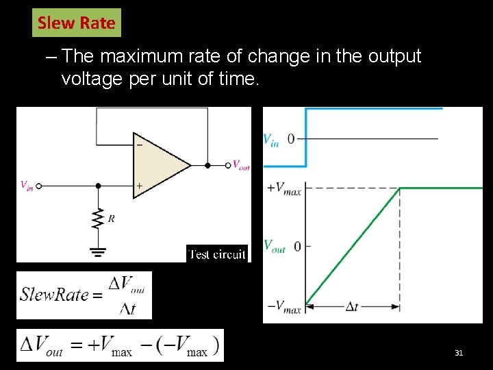
Slew Rate – The maximum rate of change in the output voltage per unit of time. 31

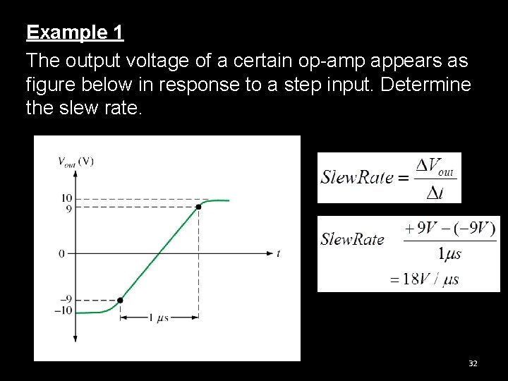
Example 1 The output voltage of a certain op-amp appears as figure below in response to a step input. Determine the slew rate. 32

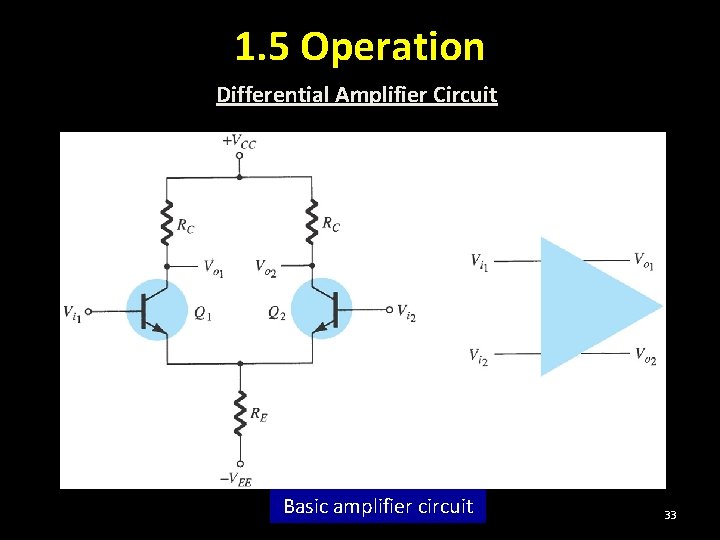
1. 5 Operation Differential Amplifier Circuit Basic amplifier circuit 33

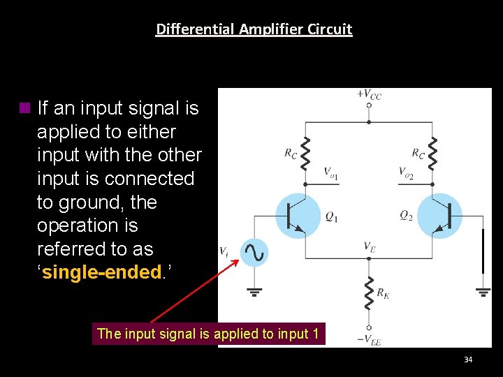
Differential Amplifier Circuit n If an input signal is applied to either input with the other input is connected to ground, the operation is referred to as ‘single-ended. ’ The input signal is applied to input 1 34

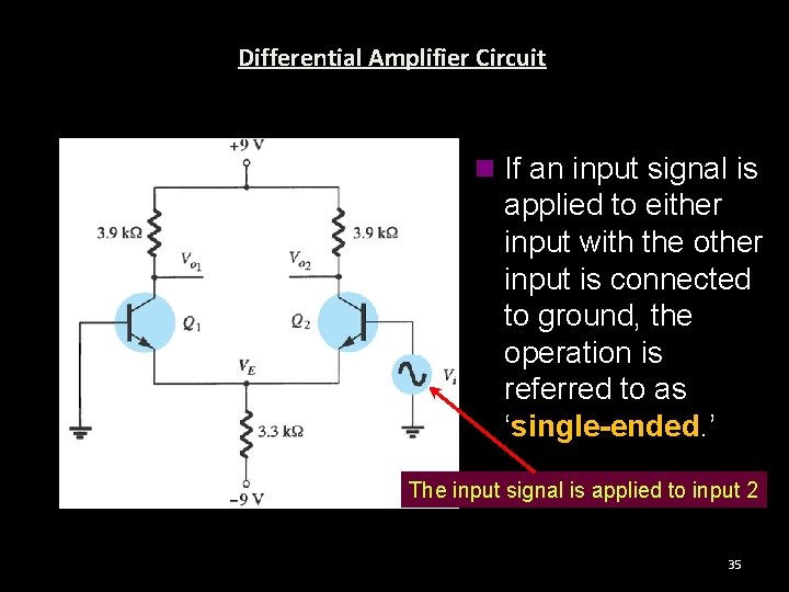
Differential Amplifier Circuit n If an input signal is applied to either input with the other input is connected to ground, the operation is referred to as ‘single-ended. ’ The input signal is applied to input 2 35

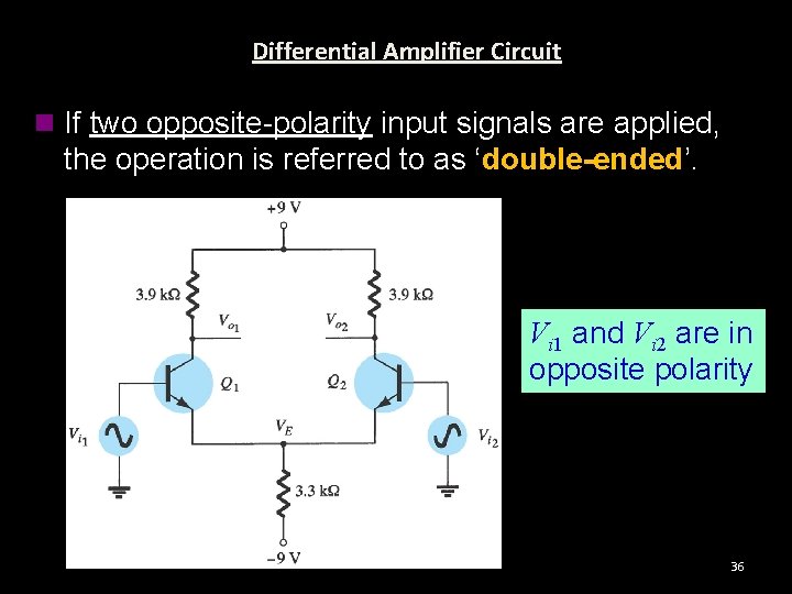
Differential Amplifier Circuit n If two opposite-polarity input signals are applied, the operation is referred to as ‘double-ended’. Vi 1 and Vi 2 are in opposite polarity 36

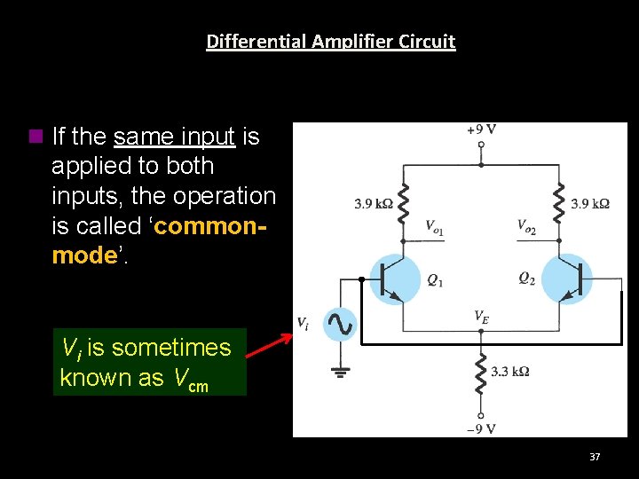
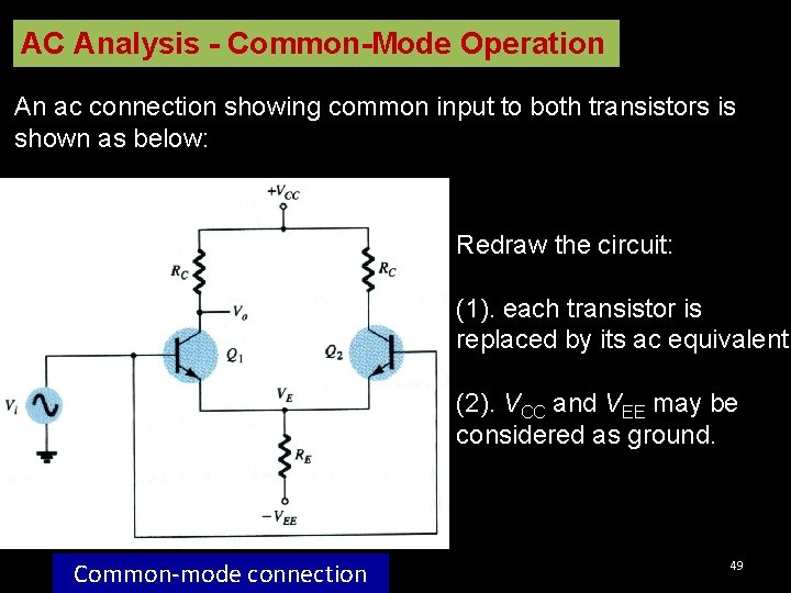
Differential Amplifier Circuit n If the same input is applied to both inputs, the operation is called ‘commonmode’. Vi is sometimes known as Vcm 37

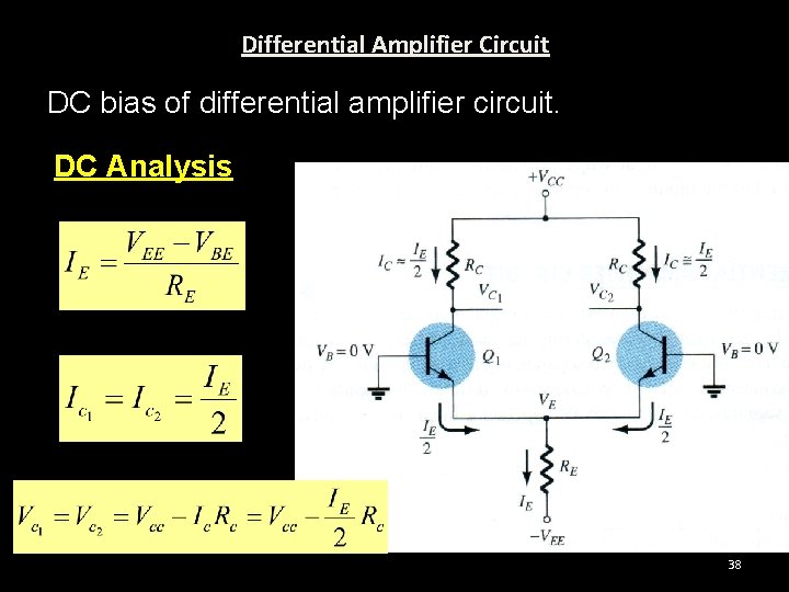
Differential Amplifier Circuit DC bias of differential amplifier circuit. DC Analysis 38

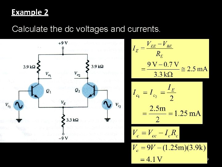
Example 2 Calculate the dc voltages and currents. 39

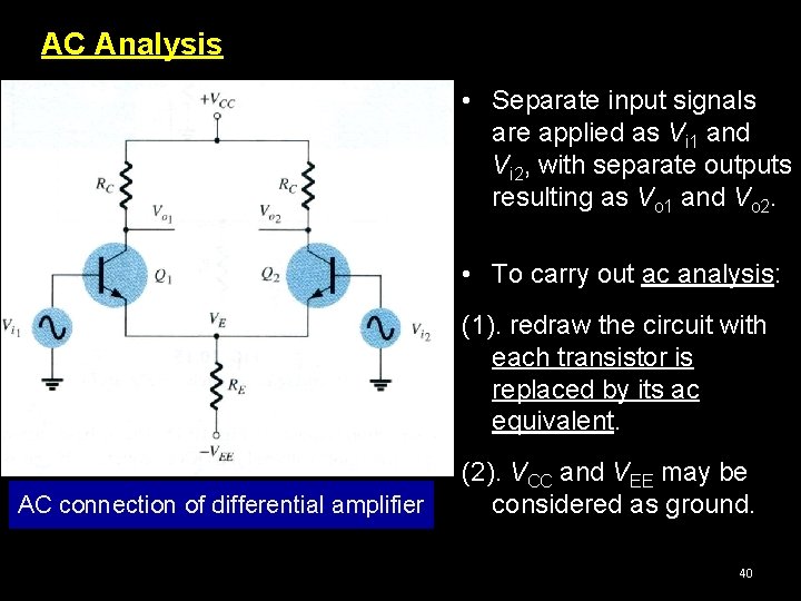
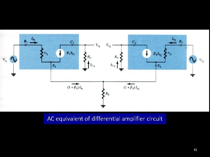
AC Analysis • Separate input signals are applied as Vi 1 and Vi 2, with separate outputs resulting as Vo 1 and Vo 2. • To carry out ac analysis: (1). redraw the circuit with each transistor is replaced by its ac equivalent. AC connection of differential amplifier (2). VCC and VEE may be considered as ground. 40

AC equivalent of differential amplifier circuit 41

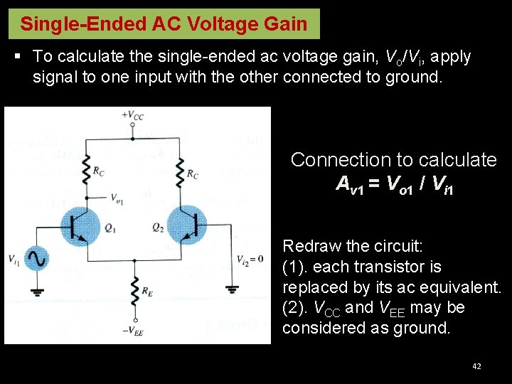
Single-Ended AC Voltage Gain § To calculate the single-ended ac voltage gain, Vo/Vi, apply signal to one input with the other connected to ground. Connection to calculate Av 1 = Vo 1 / Vi 1 Redraw the circuit: (1). each transistor is replaced by its ac equivalent. (2). VCC and VEE may be considered as ground. 42

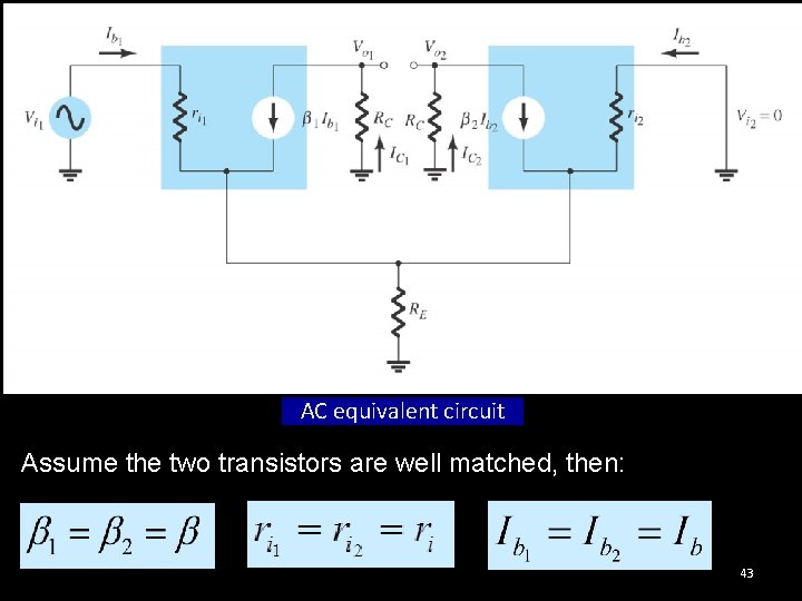
AC equivalent circuit Assume the two transistors are well matched, then: 43

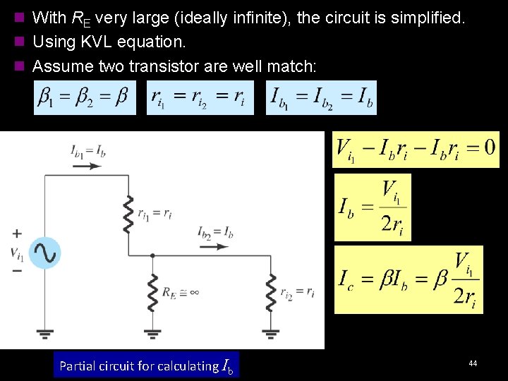
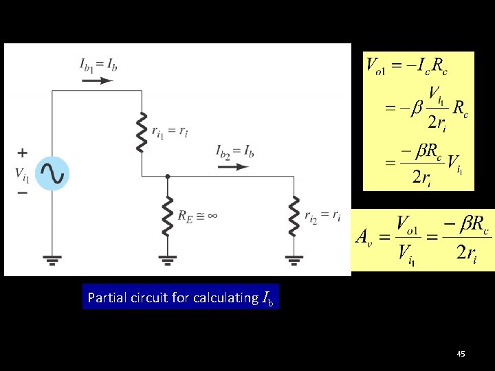
n With RE very large (ideally infinite), the circuit is simplified. n Using KVL equation. n Assume two transistor are well match: Partial circuit for calculating Ib 44

Partial circuit for calculating Ib 45

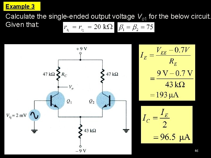
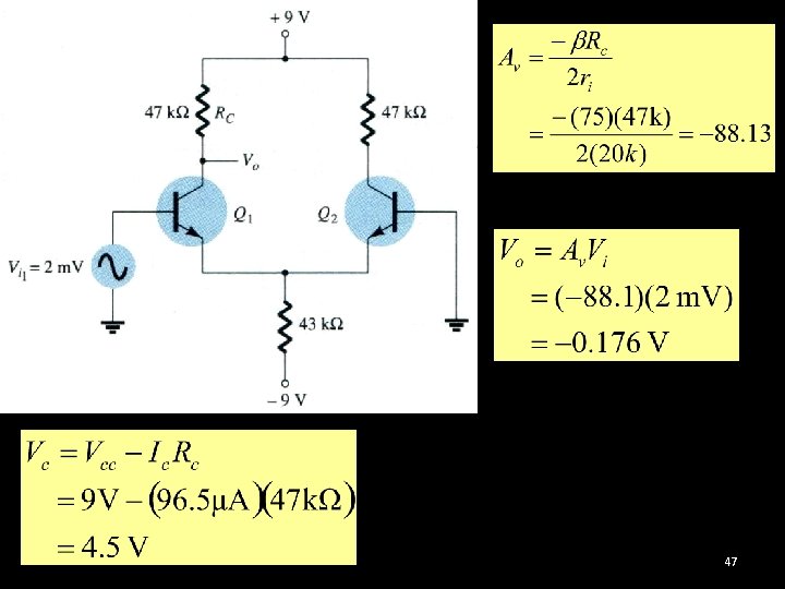
Example 3 Calculate the single-ended output voltage Vo 1 for the below circuit. Given that: 46

47

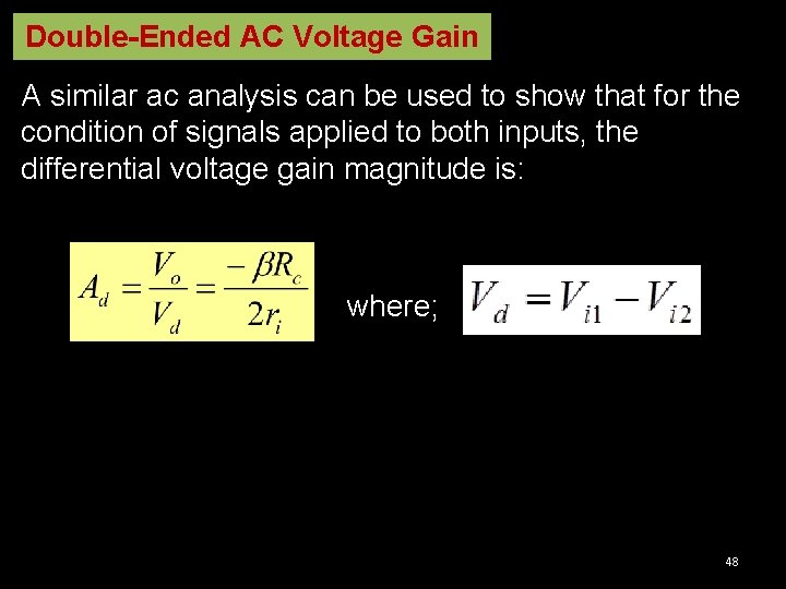
Double-Ended AC Voltage Gain A similar ac analysis can be used to show that for the condition of signals applied to both inputs, the differential voltage gain magnitude is: where; 48

AC Analysis - Common-Mode Operation An ac connection showing common input to both transistors is shown as below: Redraw the circuit: (1). each transistor is replaced by its ac equivalent. (2). VCC and VEE may be considered as ground. Common-mode connection 49

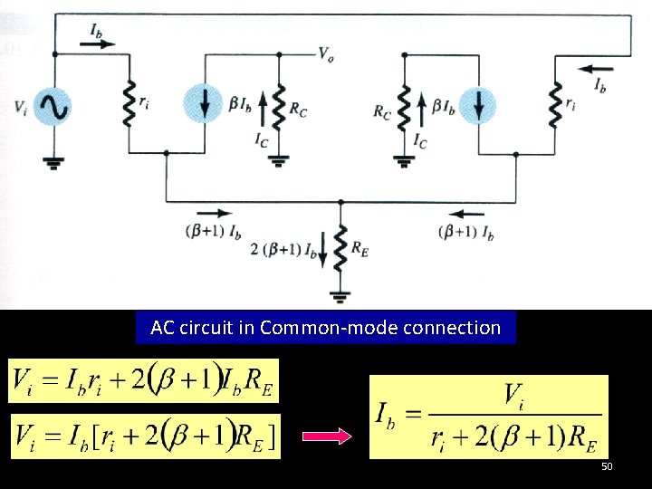
AC circuit in Common-mode connection 50

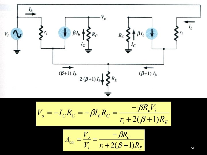
51

1. 6 Op-Amp Basics Basic Op-amp Note: Terminals for dc supply are omitted 52

AC equivalent of Op-amp Circuit Practical Ideal 53

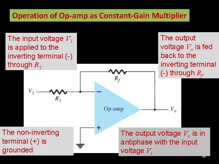
Operation of Op-amp as Constant-Gain Multiplier The input voltage V 1 is applied to the inverting terminal (-) through R 1. The non-inverting terminal (+) is grounded The output voltage Vo is fed back to the inverting terminal (-) through Rf. The output voltage Vo is in antiphase with the input voltage Vi 54

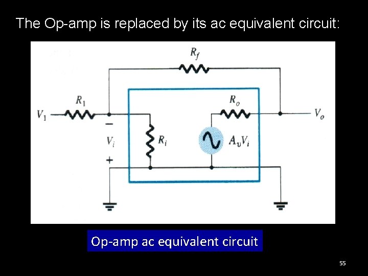
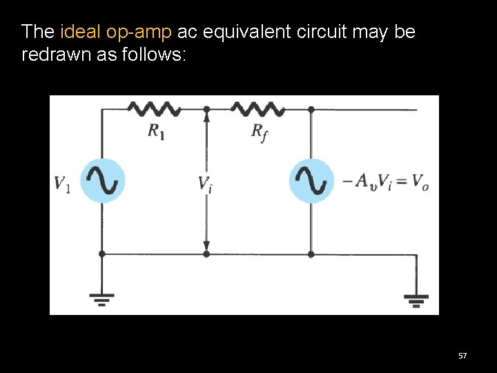
The Op-amp is replaced by its ac equivalent circuit: Op-amp ac equivalent circuit 55

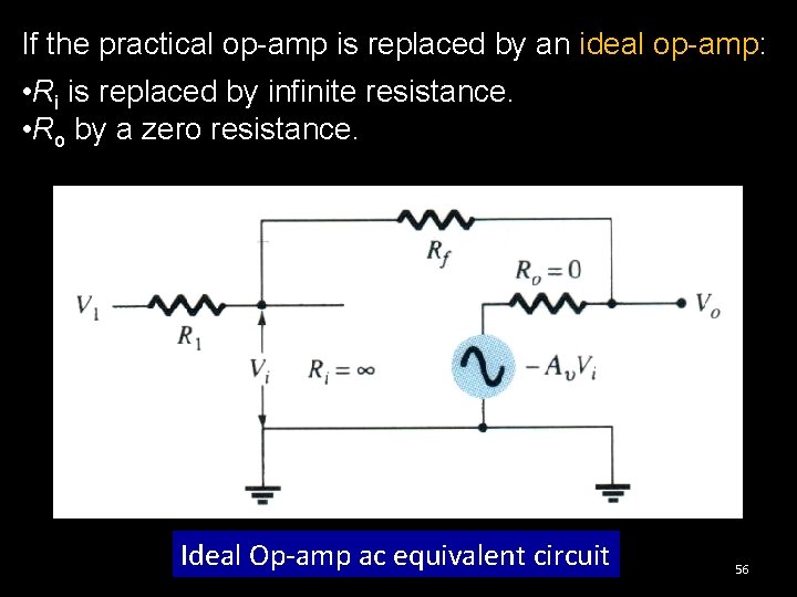
If the practical op-amp is replaced by an ideal op-amp: • Ri is replaced by infinite resistance. • Ro by a zero resistance. Ideal Op-amp ac equivalent circuit 56

The ideal op-amp ac equivalent circuit may be redrawn as follows: 57

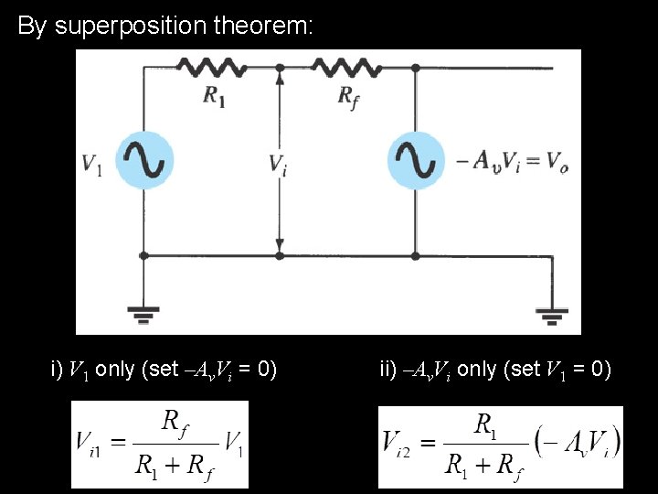
By superposition theorem: i) V 1 only (set –Av. Vi = 0) ii) –Av. Vi only (set V 1 = 0) 58

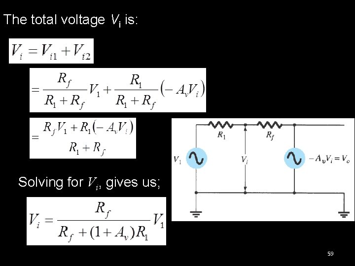
The total voltage Vi is: Solving for Vi, gives us; 59

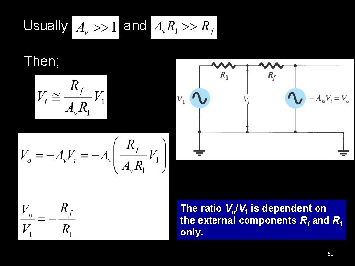
Usually and Then; The ratio Vo/V 1 is dependent on the external components Rf and R 1 only. 60

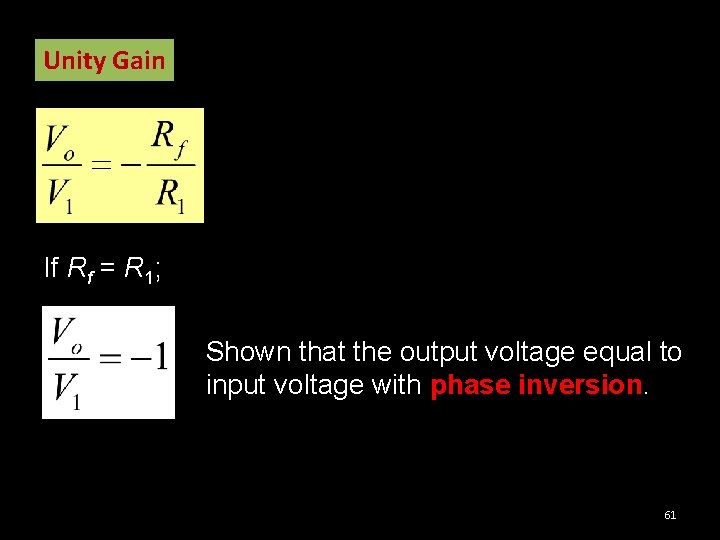
Unity Gain If Rf = R 1; Shown that the output voltage equal to input voltage with phase inversion. 61

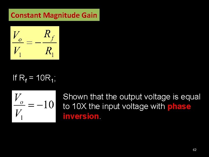
Constant Magnitude Gain If Rf = 10 R 1; Shown that the output voltage is equal to 10 X the input voltage with phase inversion. 62

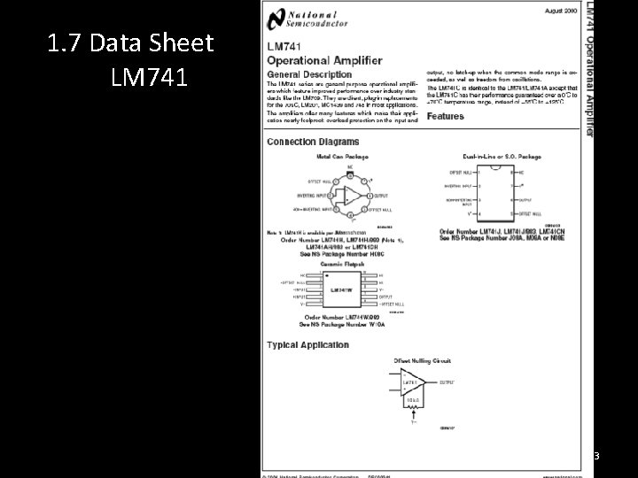
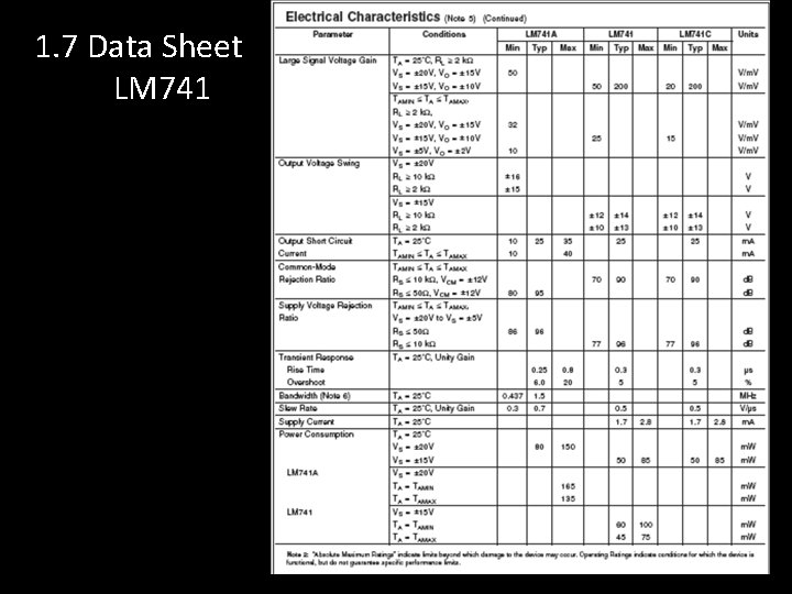
1. 7 Data Sheet LM 741 63

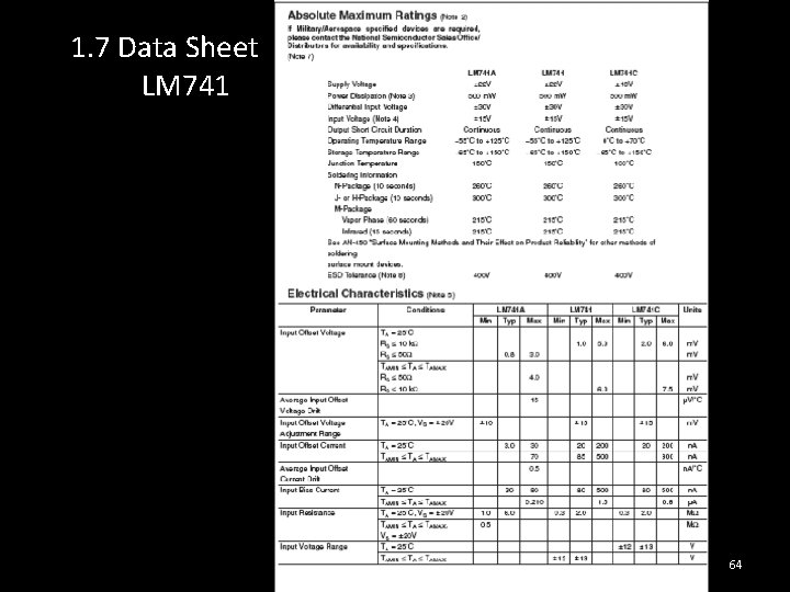
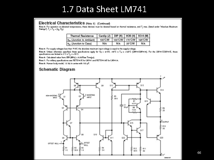
1. 7 Data Sheet LM 741 64

1. 7 Data Sheet LM 741 65

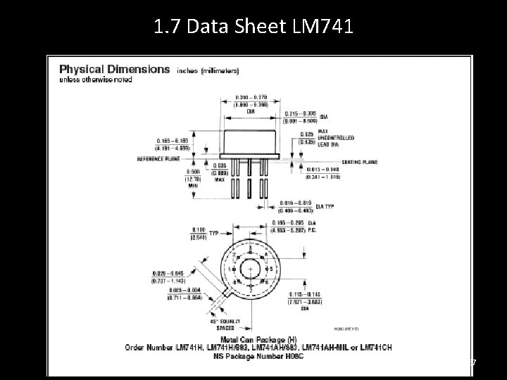
1. 7 Data Sheet LM 741 66

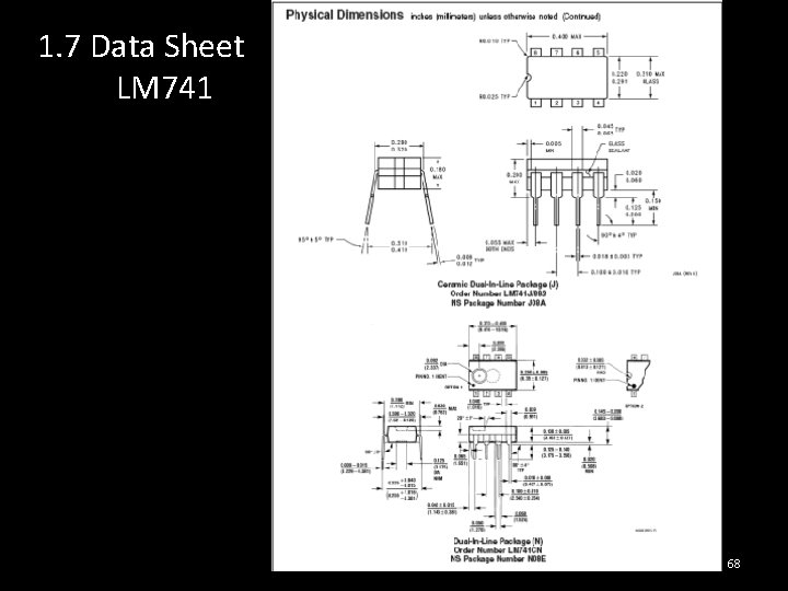
1. 7 Data Sheet LM 741 67

1. 7 Data Sheet LM 741 68

14/07/08 69