Operational amplifier Operational amplifier or simply Op Amp
- Slides: 20

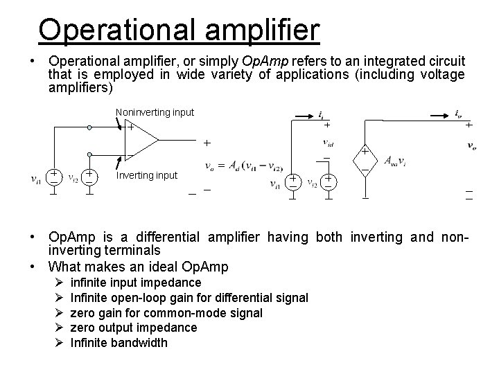
Operational amplifier • Operational amplifier, or simply Op. Amp refers to an integrated circuit that is employed in wide variety of applications (including voltage amplifiers) Noninverting input Inverting input • Op. Amp is a differential amplifier having both inverting and noninverting terminals • What makes an ideal Op. Amp Ø Ø Ø infinite input impedance Infinite open-loop gain for differential signal zero gain for common-mode signal zero output impedance Infinite bandwidth

Summing point constraint • In a negative feedback configuration, the feedback network returns a fraction fo the output to the inverting input terminal, forcing the differential input voltage toward zero. Thus, the input current is also zero. • We refer to the fact that differential input voltage and the input current are forced to zero as the summing point constraint • Steps to analyze ideal Op. Amp-based amplifier circuits Ø Verify that negative feedback is present Ø Assume summing point constraints Ø Apply Kirchhoff’s law or Ohm’s law

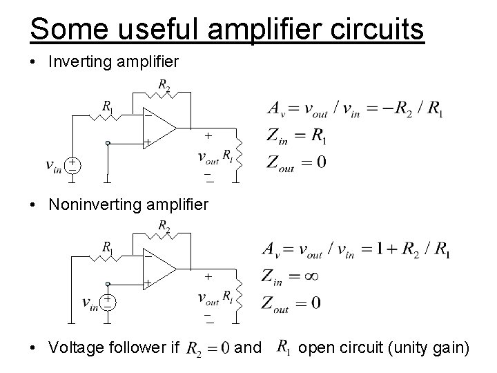
Some useful amplifier circuits • Inverting amplifier • Noninverting amplifier • Voltage follower if and open circuit (unity gain)

Amplifier design using Op. Amp • Resistance value of resistor used in amplifiers are preferred in the range of (1 K, 1 M)ohm (this may change depending on the IC technology). Small resistance might induce too large current and large resistance consumes too much chip area.

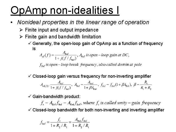
Op. Amp non-idealities I • Nonideal properties in the linear range of operation Ø Finite input and output impedance Ø Finite gain and bandwidth limitation ü Generally, the open-loop gain of Op. Amp as a function of frequency is ü Closed-loop gain versus frequency for non-inverting amplifier ü Gain-bandwidth product: ü Closed-loop bandwidth for both non-inverting and inverting amplifier

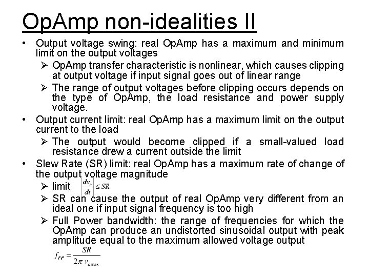
Op. Amp non-idealities II • Output voltage swing: real Op. Amp has a maximum and minimum limit on the output voltages Ø Op. Amp transfer characteristic is nonlinear, which causes clipping at output voltage if input signal goes out of linear range Ø The range of output voltages before clipping occurs depends on the type of Op. Amp, the load resistance and power supply voltage. • Output current limit: real Op. Amp has a maximum limit on the output current to the load Ø The output would become clipped if a small-valued load resistance drew a current outside the limit • Slew Rate (SR) limit: real Op. Amp has a maximum rate of change of the output voltage magnitude Ø limit Ø SR can cause the output of real Op. Amp very different from an ideal one if input signal frequency is too high Ø Full Power bandwidth: the range of frequencies for which the Op. Amp can produce an undistorted sinusoidal output with peak amplitude equal to the maximum allowed voltage output

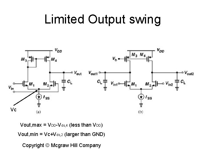
Limited Output swing Vc Vout, max = VDD-Vds, 4 (less than VDD) Vout, min = Vc+Vds, 2 (larger than GND) Copyright © Mcgraw Hill Company

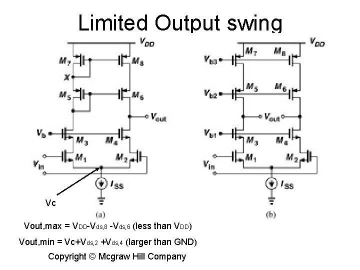
Limited Output swing Vc Vout, max = VDD-Vds, 8 -Vds, 6 (less than VDD) Vout, min = Vc+Vds, 2 +Vds, 4 (larger than GND) Copyright © Mcgraw Hill Company

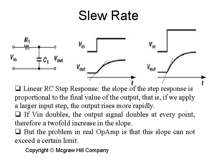
Slew Rate q Linear RC Step Response: the slope of the step response is proportional to the final value of the output, that is, if we apply a larger input step, the output rises more rapidly. q If Vin doubles, the output signal doubles at every point, therefore a twofold increase in the slope. q But the problem in real Op. Amp is that this slope can not exceed a certain limit. Copyright © Mcgraw Hill Company

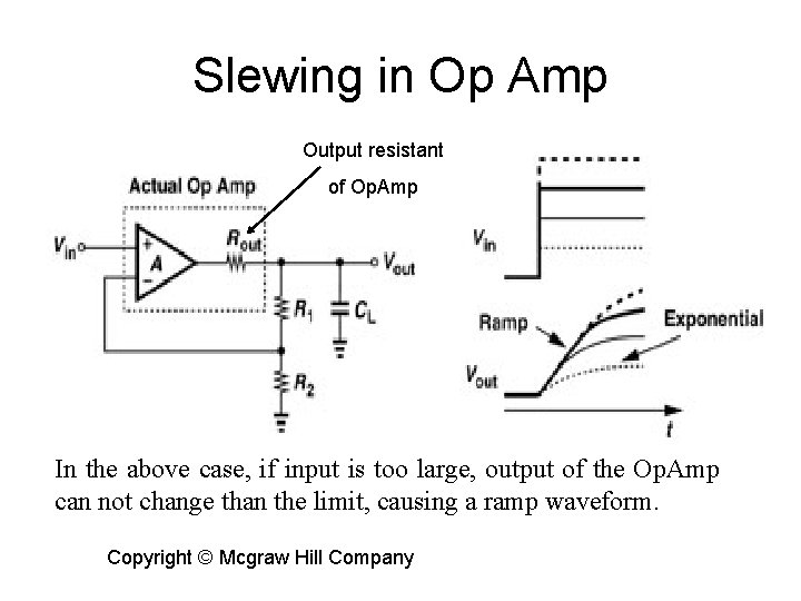
Slewing in Op Amp Output resistant of Op. Amp In the above case, if input is too large, output of the Op. Amp can not change than the limit, causing a ramp waveform. Copyright © Mcgraw Hill Company

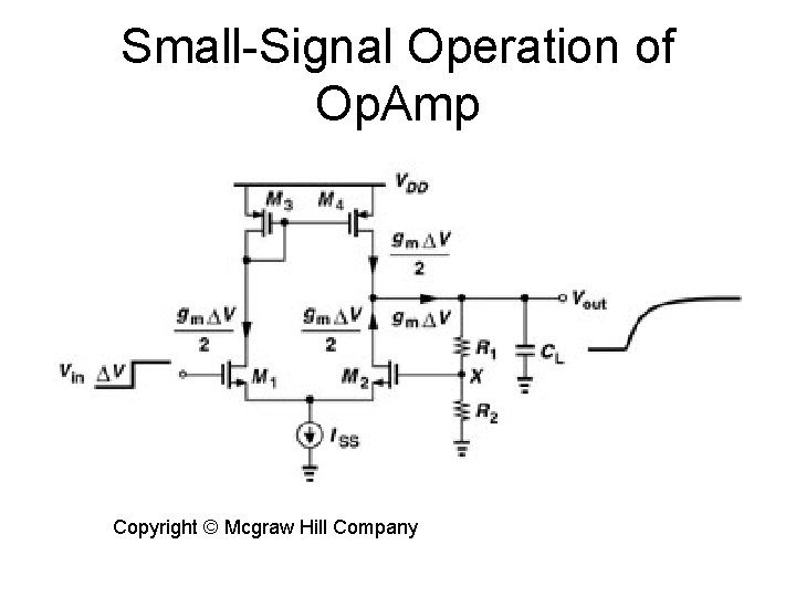
Small-Signal Operation of Op. Amp Copyright © Mcgraw Hill Company

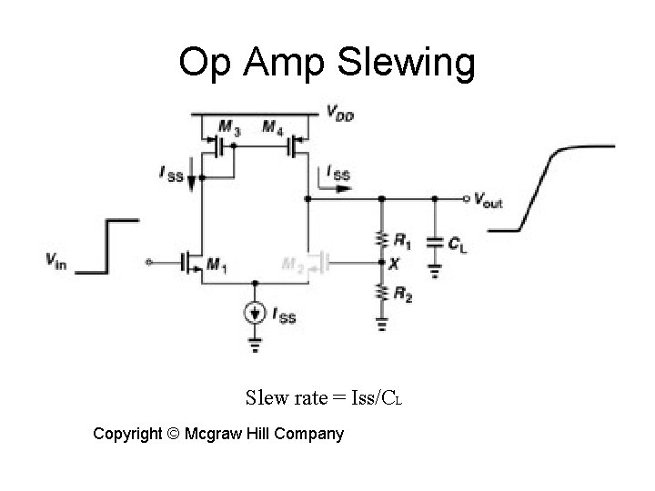
Op Amp Slewing Slew rate = Iss/CL Copyright © Mcgraw Hill Company

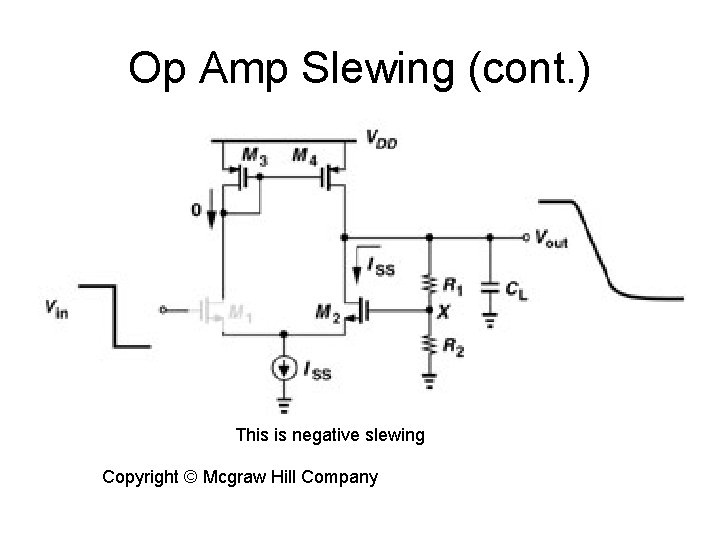
Op Amp Slewing (cont. ) This is negative slewing Copyright © Mcgraw Hill Company

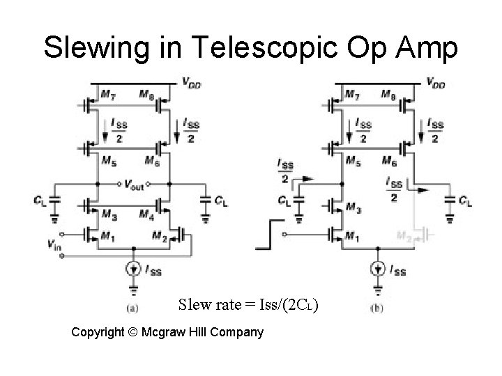
Slewing in Telescopic Op Amp Slew rate = Iss/(2 CL) Copyright © Mcgraw Hill Company

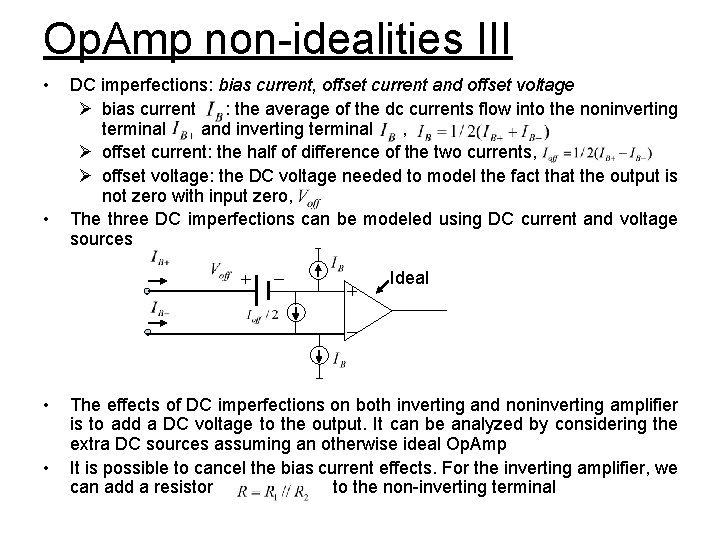
Op. Amp non-idealities III • • DC imperfections: bias current, offset current and offset voltage Ø bias current : the average of the dc currents flow into the noninverting terminal and inverting terminal , Ø offset current: the half of difference of the two currents, Ø offset voltage: the DC voltage needed to model the fact that the output is not zero with input zero, The three DC imperfections can be modeled using DC current and voltage sources Ideal • • The effects of DC imperfections on both inverting and noninverting amplifier is to add a DC voltage to the output. It can be analyzed by considering the extra DC sources assuming an otherwise ideal Op. Amp It is possible to cancel the bias current effects. For the inverting amplifier, we can add a resistor to the non-inverting terminal

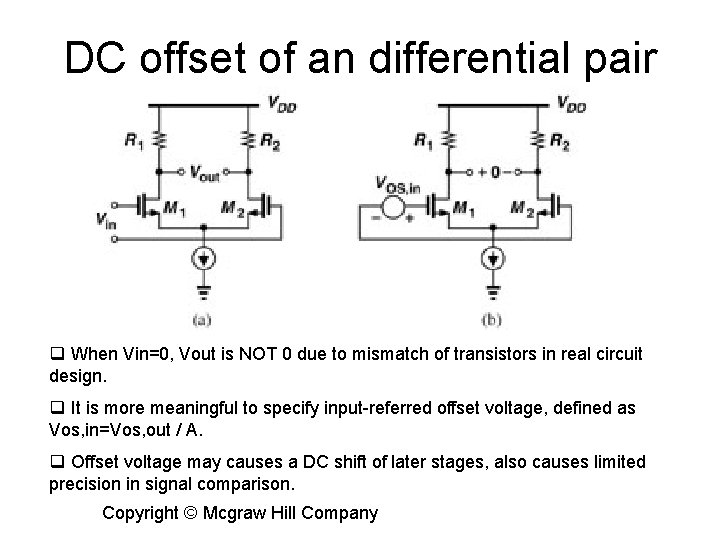
DC offset of an differential pair q When Vin=0, Vout is NOT 0 due to mismatch of transistors in real circuit design. q It is more meaningful to specify input-referred offset voltage, defined as Vos, in=Vos, out / A. q Offset voltage may causes a DC shift of later stages, also causes limited precision in signal comparison. Copyright © Mcgraw Hill Company

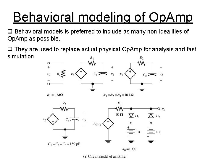
Behavioral modeling of Op. Amp q Behavioral models is preferred to include as many non-idealities of Op. Amp as possible. q They are used to replace actual physical Op. Amp for analysis and fast simulation.

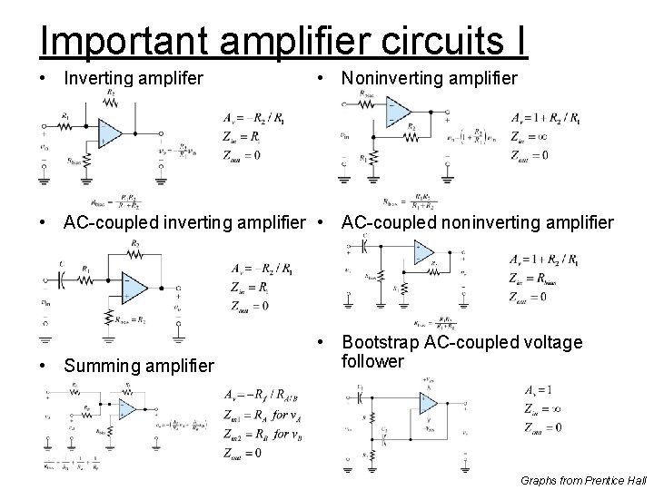
Important amplifier circuits I • Inverting amplifer • Noninverting amplifier • AC-coupled inverting amplifier • AC-coupled noninverting amplifier • Summing amplifier • Bootstrap AC-coupled voltage follower Graphs from Prentice Hall

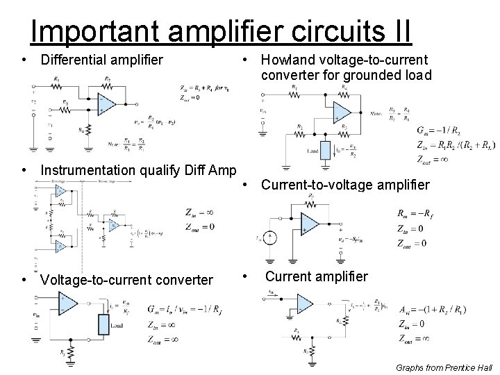
Important amplifier circuits II • Differential amplifier • Instrumentation qualify Diff Amp • Voltage-to-current converter • Howland voltage-to-current converter for grounded load • Current-to-voltage amplifier • Current amplifier Graphs from Prentice Hall

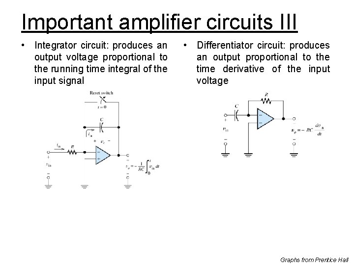
Important amplifier circuits III • Integrator circuit: produces an output voltage proportional to the running time integral of the input signal • Differentiator circuit: produces an output proportional to the time derivative of the input voltage Graphs from Prentice Hall