Operational Amplifier Op Amp Overview Amplifier impedance The


 is made of many transistors, diodes, resistors and")


;")


 — provides high voltage gain, a single-pole frequency rolloff,")


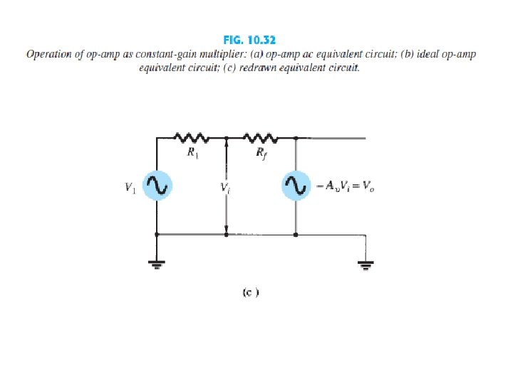
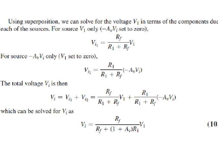
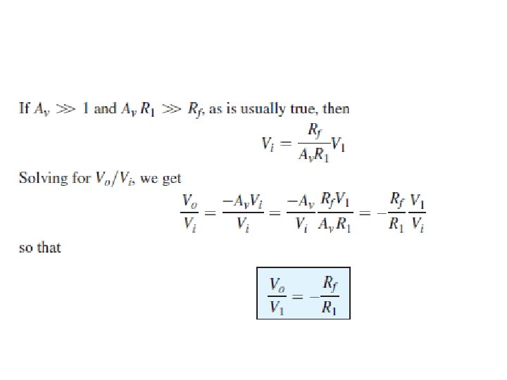


 Kirchhoff node equation at V+ yields, (2) Kirchhoff node equation at")

 • So v. O=v. IN")


 Kirchhoff node equation at V+ yields, (2) Kirchhoff node equation at")


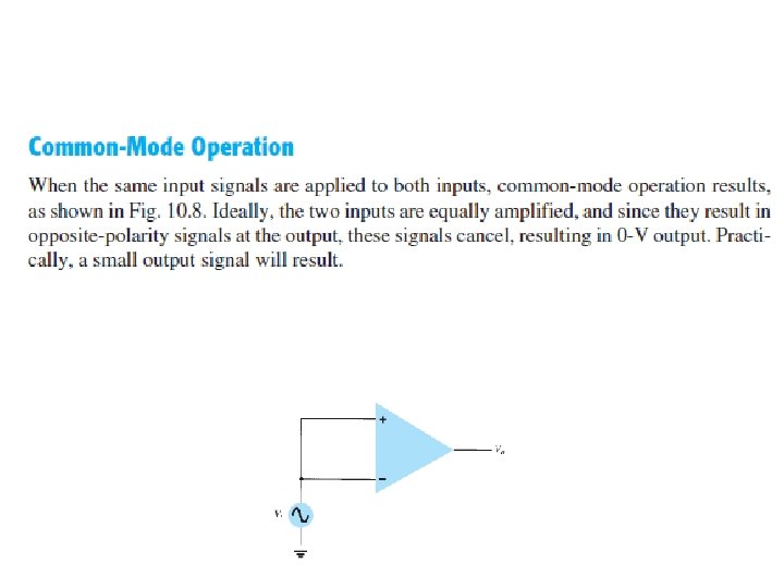
 Useful terms: • if both inputs change together, this is a")

- Slides: 64
Operational Amplifier Op. Amp
Overview • • • Amplifier impedance The operational amplifier Ideal op-amp Negative feedback Applications – Amplifiers – Summing/ subtracting circuits
Impedances • Why do we care about the input and output impedance? • Simplest "black box" amplifier model: ROUT VIN RIN AVIN VOUT • The amplifier measures voltage across RIN, then generates a voltage which is larger by a factor A • This voltage generator, in series with the output resistance ROUT, is connected to the output port. • A should be a constant (i. e. , gain is linear)
Impedances • Attach an input - a source voltage VS plus source impedance RS RS VS ROUT VIN RIN AVIN VOUT • Note the voltage divider RS + RIN. • VIN=VS(RIN/(RIN+RS) • We want VIN = VS regardless of source impedance • So want RIN to be large. Q: What would be the input impedance of an ‘ideal amplifier’? The ideal amplifier has an infinite input impedance
Impedances Attach a load - an output circuit with a resistance RL RS VS ROUT VIN RIN AVIN VOUT RL • Note the voltage divider ROUT + RL. • VOUT=AVIN(RL/(RL+ROUT)) • Want VOUT=AVIN regardless of load • We want ROUT to be small. Q: What would be the output impedance of an ‘ideal amplifier’? The ideal amplifier has zero output impedance
Operational Amplifier • Integrated circuit containing ~20 transistors, multiple amplifier stages
Ideal Operational Amplifier Operational amplifier (Op-amp) is made of many transistors, diodes, resistors and capacitors in integrated circuit technology. Ideal op-amp is characterized by: §Infinite input impedance §Infinite gain for differential input §Zero output impedance §Infinite frequency bandwidth
Operational Amplifier • An op amp is a high voltage gain, DC amplifier with high input impedance, low output impedance, and differential inputs. • Positive input at the non-inverting input produces positive output • Positive input at the inverting input produces negative output.
741 Op Amp IC
A component-level diagram of the common 741 op-amp. Dotted lines outline: current mirrors (red); differential amplifier (blue); class A gain stage (magenta); voltage level shifter (green); output stage (cyan).
IC Product DIP-741 Dual op-amp 1458 device Operational Amplifier 11
A small-scale integrated circuit, the 741 opamp shares with most op-amps an internal structure consisting of three gain stages: 1. Differential amplifier (outlined blue) — provides high differential amplification (gain), with rejection of common-mode signal, low noise, high input impedance
2. Voltage amplifier (outlined magenta) — provides high voltage gain, a single-pole frequency rolloff, and in turn drives the 3. Output amplifier (outlined cyan and green) — provides high current gain (low output impedance), along with output current limiting, and output short-circuit protection. Additionally, it contains current mirror (outlined red) bias circuitry and a gain-stabilization capacitor (30 p. F).
Op Amp Equivalent Circuit vd = v 2 – v 1 v 2 A is the open-loop voltage gain v 1 Voltage controlled voltage source
Operational Amplifier • Can model any amplifier as a "black-box" with a parallel input impedance Rin, and a voltage source with gain Av in series with an output impedance Rout.
Ideal op-amp • Place a source and a load on the model RS + vout RL - • Infinite internal resistance Rin (so vin=vs). • Zero output resistance Rout (so vout=Avvin). • "A" very large • iin=0; no current flow into op-amp So the equivalent circuit of an ideal op-amp looks like this:
Ideal vs. Real op-amps!
Symbols for Ideal and Real Op Amps Op. Amp u. A 741 LM 111 LM 324
Ideal Vs Practical Op-Amp Ideal Practical Open Loop gain A 105 Bandwidth BW 10 -100 Hz Input Impedance Zin >1 M 0 10 -100 Output Impedance Zout Output Voltage Vout CMRR Ref: 080114 HKN Depends only on Vd = (V+ V ) Differential mode signal Depends slightly on average input Vc = (V++V )/2 Common-Mode signal 10 -100 d. B Operational Amplifier 19
Typical Op Amp Parameters Parameter Variable Typical Ranges Ideal Values Open-Loop Voltage Gain A 105 to 108 ∞ Input Resistance Ri 105 to 1013 ∞ Output Resistance Ro 10 to 100 0 Supply Voltage Vcc/V+ -Vcc/V- 5 to 30 V -30 V to 0 V N/A
Almost Ideal Op Amp • Ri = ∞ – Therefore, i 1 = i 2 = 0 A • Ro = 0 • Usually, vd = 0 V so v 1 = v 2 – The op amp forces the voltage at the inverting input terminal to be equal to the voltage at the noninverting input terminal if there is some component connecting the output terminal to the inverting input terminal. • Rarely is the op amp limited to V- < vo < V+. – The output voltage is allowed to be as positive or as negative as needed to force vd = 0 V.
Many Applications, e. g. , • • • Amplifiers Adders and subtractors Integrators and differentiators Clock generators Active Filters Digital-to-analog converters
Applications • Audio amplifiers – Speakers and microphone circuits in cell phones, computers, mpg players, boom boxes, etc. • Instrumentation amplifiers – Biomedical systems including heart monitors and oxygen sensors. • Power amplifiers • Analog computers – Combination of integrators, differentiators, summing amplifiers, and multipliers
Applications Originally developed for use in analog computers:
Using op-amps • Power the op-amp and apply a voltage • Works as an amplifier, but: • No flexibility (A~105 -6) • Exact gain is unreliable (depends on chip, frequency and temp) • Saturates at very low input voltages (Max vout=power supply voltage) • To operate as an amp, v+-v-<VS/A=12/105 so v+≈v • In the ideal case, when an op-amp is functioning properly in the active region, the voltage difference between the inverting and noninverting inputs≈0
Voltage Transfer Characteristic Range where we operate the op amp as an amplifier. vd
Inverting Apmlifier
Non-inverting amplifier
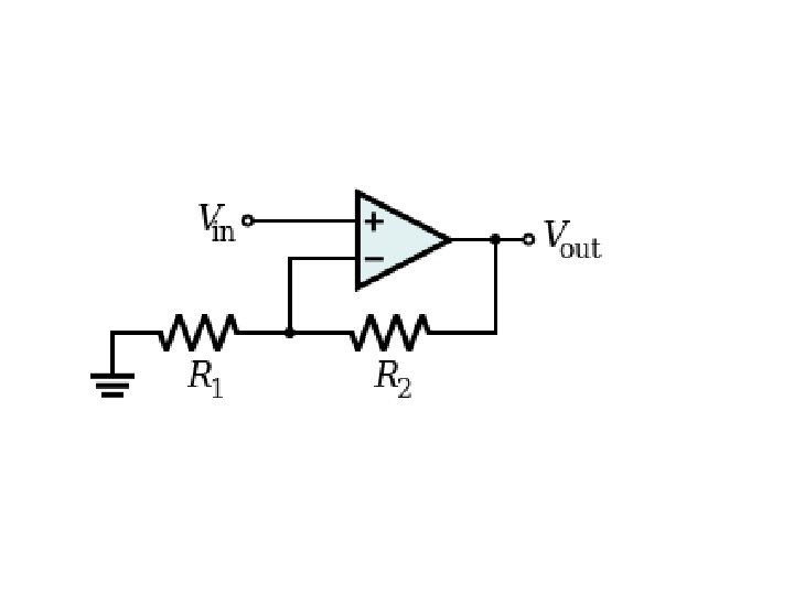
Noninverting Amplifier
When A is very large: Take A=106, R 1=9 R, R 2=R >>1 • Gain now determined only by resistance ratio • Doesn’t depend on A, (or temperature, frequency, variations in fabrication)
Negative feedback: • How did we get to stable operation in the linear amplification region? ? ? • Feed a portion of the output signal back into the input (feeding it back into the inverting input = negative feedback) • This cancels most of the input • Maintains (very) small differential signal at input • Reduces the gain, but if the open loop gain is ~ , who cares? • Good discussion of negative feedback here: http: //www. allaboutcircuits. com/vol_3/chpt_8/4. html
Why use Negative feedback? : • Helps to overcome distortion and non-linearity • Improves the frequency response • Makes properties predictable - independent of temperature, manufacturing differences or other properties of the op. Amp • Circuit properties only depend upon the external feedback network and so can be easily controlled
Positive Feedback When we flip the polarization of the op-amp as shown on the figure we will get a positive feedback that saturates the amplifier output. This is not a good idea.
Negative vs. Positive Feedback Familiar examples of negative feedback: • Thermostat controlling room temperature • Driver controlling direction of automobile • Pupil diameter adjustment to light intensity Familiar examples of positive feedback: • Microphone “squawk” in sound system • Mechanical bi-stability in light switches EE 42/100 Fall 2005 Week 8, Prof. White Fundamentally pushes toward stability Fundamentally pushes toward instability or bi-stability 48
Noninverting amplifier Voltage follower Ref: 080114 HKN Noninverting input with voltage divider Less than unity gain Operational Amplifier 49
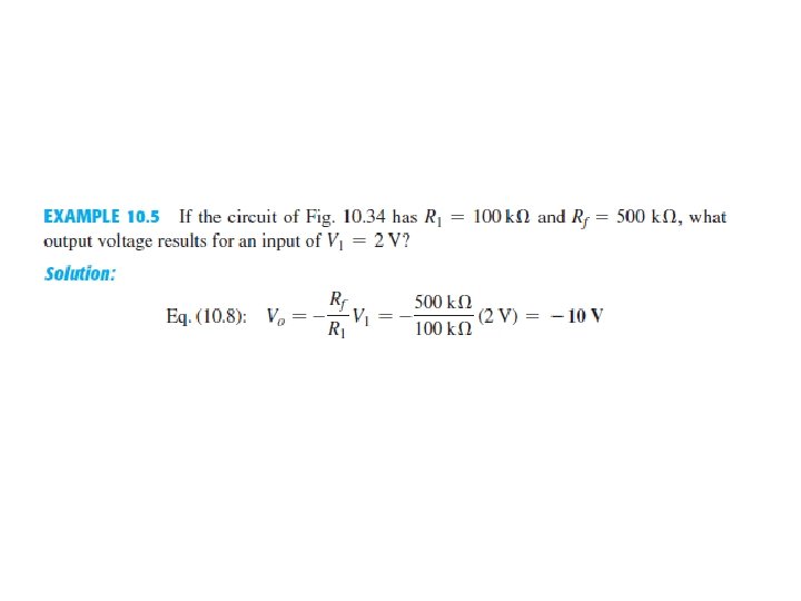
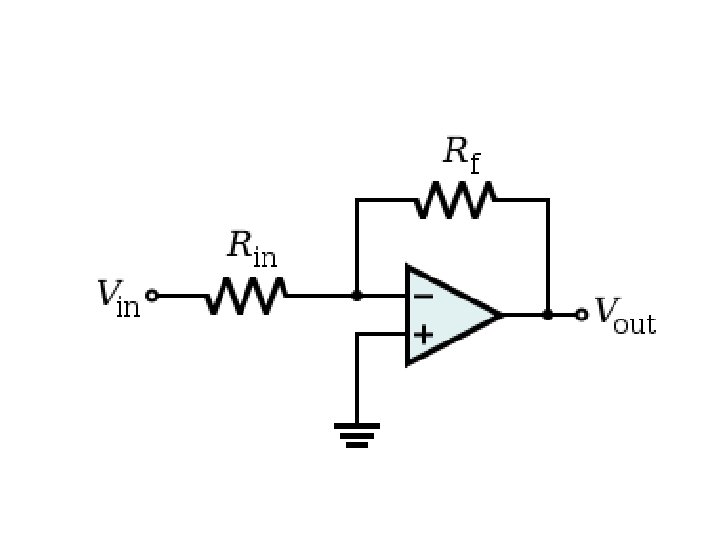
Inverting Amplifier (1) Kirchhoff node equation at V+ yields, (2) Kirchhoff node equation at V yields, (3) Setting V+ = V– yields Ref: 080114 HKN Notice: The closed-loop gain Vo/Vin is dependent upon the ratio of two resistors, and is independent of the open-loop gain. This is caused by the use of feedback output voltage to subtract from the input voltage. Operational Amplifier 50
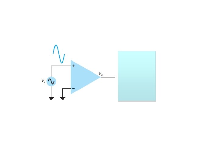
Op amp circuit 1: Voltage follower • So v. O=v. IN • or, using equations • What's the gain of this circuit?
Op amp circuit 1: Voltage follower (unity buffer amplifier) • So v. O=v. IN • or, using equations • What's the application of this circuit? • Buffer Useful interface between different circuits: voltage gain = 1 Has minimum effect on previous and next input impedance=∞ circuit in signal chain output impedance=0 RS VS ROUT VIN RIN AVIN VOUT RL
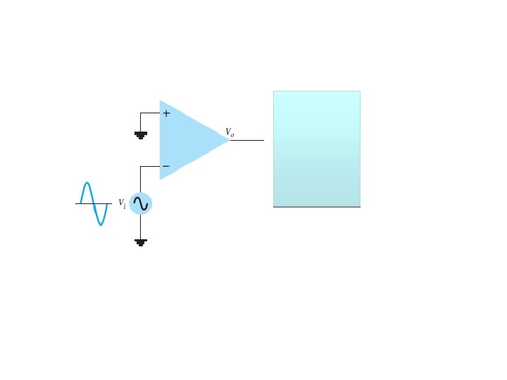
Voltage Follower Special case of noninverting amplifier is a voltage follower Since in the noninverting amplifier vo = v 1(1+ R 2 /R 1) so when R 2=0 vo = v 1 =>
Op amp circuit 2: Inverting Amplifier • Signal and feedback resistor, connected to inverting (-) input. • v+=v- connected to ground v+ grounded, so:
Op amp circuit 3: Summing Amplifier • Same as previous, but add more voltage sources
Multiple Inputs (1) Kirchhoff node equation at V+ yields, (2) Kirchhoff node equation at V yields, (3) Setting V+ = V– yields Ref: 080114 HKN Operational Amplifier 58
Summing Amplifier Circuit Ra ib + – + ic vc – + vb in Rc vn + vp – – + va Rb Rf if – ia + vo – superposition ! in = 0 ia + ib + ic = -if vp = 0 vn = 0 EE 42/100 Fall 2005 Week 8, Prof. White 59
Summing Amplifier Applications • Applications - audio mixer • Adds signals from a number of waveforms • http: //wiredworld. tripod. com/tronics/mixer. html • Can use unequal resistors to get a weighted sum • For example - could make a 4 bit binary - decimal converter • 4 inputs, each of which is +1 V or zero • Using input resistors of 10 k (ones), 5 k (twos), 2. 5 k (fours) and 1. 25 k (eights)
Another non-inverting amplifier • Feedback resistor still to inverting input, but no voltage source on inverting input (note change of current flow) • Input voltage to non-inverting input
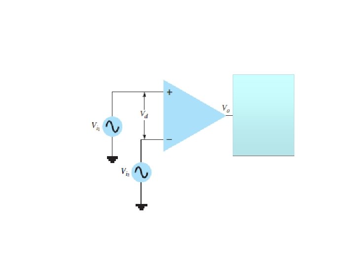
Differential Amplifier (subtractor) Useful terms: • if both inputs change together, this is a common-mode input change • if they change independently, this is a normal-mode change • A good differential amp has a high common-mode rejection ratio (CMMR)
Amplifies the difference in voltage between its inputs. The name "differential amplifier" must not be confused with the "differentiator”