Electronics Devices Circuits UNIT1 Multistage amplifier Multistage amplifier


 • The")


 of the")


 of the")


- Slides: 106
Electronics Devices & Circuits
UNIT-1 Multistage amplifier
Multistage amplifier • To increases the voltage gain of the amplifier, multiple amplifier are connects in cascade. The output of one amplifier is the input to another stage. In this way the overall voltage gain can be increased, when number of amplifier stages are used in succession it is called a multistage amplifier or cascade amplifier. • The load on the first amplifier is the input resistance of the second amplifier. The various stages need not have the same voltage and current gain. In practice, the earlier stages are often voltage amplifiers and the last one or two stages are current amplifiers. • The voltage amplifier stages assure that the current stages have the proper input swing. The amount of gain in a stage is determined by the load on the amplifier stage, which is governed by the input resistance to the next stage. • Therefore, in designing or analysing multistage amplifier, we start at the output and proceed toward the input.
A n-stage amplifier can be represented by the block diagram as shown in fig. The overall voltage gain is the product of the voltage gain of each stage. A = A 1×A 2 ×………× An.
Gain in d. B • To represent the gain of the cascade amplifier, the voltage gains are represents in d. B. The two power levels of input and output of an amplifier are compared on a logarithmic scale rather than linear scale. The number of bels by which the output power P 2 exceeds the input power P 1 is defined as
Because of d. B scale the gain can be directly added when a number of stages are cascaded.
Types of Coupling • • The three couplings generally used are. RC coupling Impedance coupling Transformer coupling.
RC coupling • RC coupling the most commonly used method of coupling from one stage to the next. An ac source with a source resistance Rs drives the input of an amplifier. The grounded emitter stage amplifies the signal, which is then coupled to next CE stage the signal is further amplified to get larger output. • In this case the signal developed across the collector resistor of each stage is coupled into the base of the next stage. The cascaded stages amplify the signal and the overall gain equals the product of the individual gains.
RC coupling
RC coupling • The coupling capacitors pass ac but block dc Because of this the stages are isolated as for as dc is concerned. This is necessary to avoid shifting of Q-points. The drawback of this approach is the lower frequency limit imposed by the coupling capacitor. • The bypass capacitors are needed because they bypass the emitters to ground. Without them, the voltage gain of each stage would be lost. These bypass capacitors also place a lower limit on the frequency response. As the frequency keeps decreasing, a point is reached at which capacitors no longer look like a. c. shorts. At this frequency the voltage gain starts to decrease because of the local feedback and the overall gain of the amplifier drops significantly. These amplifiers are suitable for frequencies above 10 Hz.
Frequency response curve
Advantages of RC Coupled Amplifier: • The frequency response of RC amplifier provides constant gain over a wide frequency range, hence most suitable for audio applications. • The circuit is simple and has lower cost because it employs resistors and capacitors which are cheap. • It becomes more compact with the upgrading technology. Disadvantages of RC Coupled Amplifier: • The voltage and power gain are low because of the effective load resistance. • They become noisy with age. • Due to poor impedance matching, power transfer will be low. Applications of RC Coupled Amplifier • They have excellent audio fidelity over a wide range of frequency. • Widely used as Voltage amplifiers • Due to poor impedance matching, RC coupling is rarely used in the final stages.
Transformer Coupled Amplifier • We have observed that the main drawback of RC coupled amplifier is that the effective load resistance gets reduced. This is because, the input impedance of an amplifier is low, while its output impedance is high. • When they are coupled to make a multistage amplifier, the high output impedance of one stage comes in parallel with the low input impedance of next stage. Hence, effective load resistance is decreased. This problem can be overcome by a transformer coupled amplifier. • In a transformer-coupled amplifier, the stages of amplifier are coupled using a transformer.
Construction of Transformer Coupled Amplifier • The amplifier circuit in which, the previous stage is connected to the next stage using a coupling transformer, is called as Transformer coupled amplifier. • The coupling transformer T 1 is used to feed the output of 1 ststage to the input of 2 nd stage. The collector load is replaced by the primary winding of the transformer. • The secondary winding is connected between the potential divider and the base of 2 ndstage, which provides the input to the 2 nd stage. • Instead of coupling capacitor like in RC coupled amplifier, a transformer is used for coupling any two stages, in the transformer coupled amplifier circuit.
Circuit diagram of transformer coupled amplifier
The potential divider network R 1 and R 2 and the resistor Retogether form the biasing and stabilization network. The emitter by-pass capacitor Ce offers a low reactance path to the signal. The resistor RL is used as a load impedance. The input capacitor Cin present at the initial stage of the amplifier couples AC signal to the base of the transistor. The capacitor CC is the coupling capacitor that connects two stages and prevents DC interference between the stages and controls the shift of operating point.
Operation of Transformer Coupled Amplifier • When an AC signal is applied to the input of the base of the first transistor then it gets amplified by the transistor and appears at the collector to which the primary of the transformer is connected. • The transformer which is used as a coupling device in this circuit has the property of impedance changing, which means the low resistance of a stage (or load) can be reflected as a high load resistance to the previous stage. Hence the voltage at the primary is transferred according to the turns ratio of the secondary winding of the transformer. • This transformer coupling provides good impedance matching between the stages of amplifier. The transformer coupled amplifier is generally used for power amplification.
Frequency Response of Transformer Coupled Amplifier
• The gain of the amplifier is constant only for a small range of frequencies. The output voltage is equal to the collector current multiplied by the reactance of primary. • At low frequencies, the reactance of primary begins to fall, resulting in decreased gain. At high frequencies, the capacitance between turns of windings acts as a bypass condenser to reduce the output voltage and hence gain. • So, the amplification of audio signals will not be proportionate and some distortion will also get introduced, which is called as Frequency distortion.
Advantages • An excellent impedance matching is provided. • Gain achieved is higher. • There will be no power loss in collector and base resistors. • Efficient in operation. Disadvantages • Though the gain is high, it varies considerably with frequency. Hence a poor frequency response. • Frequency distortion is higher. • Transformers tend to produce hum noise. • Transformers are bulky and costly. Applications • Mostly used for impedance matching purposes. • Used for Power amplification. • Used in applications where maximum power transfer is needed.
Direct Coupled Amplifier • As no coupling devices are used, the coupling of the amplifier stages is done directly and hence called as Direct coupled amplifier. • especially used to amplify lower frequencies, such as amplifying photo-electric current or thermo-couple current or so.
Construction • The figure below indicates the three stage direct coupled transistor amplifier. The output of first stage transistor T 1 is connected to the input of second stage transistor T 2.
The transistor in the first stage will be an NPN transistor, while the transistor in the next stage will be a PNP transistor and so on. This is because, the variations in one transistor tend to cancel the variations in the other. The rise in the collector current and the variation in β of one transistor gets cancelled by the decrease in the other.
Operation The input signal when applied at the base of transistor T 1, it gets amplified due to the transistor action and the amplified output appears at the collector resistor Rc of transistor T 1. This output is applied to the base of transistor T 2 which further amplifies the signal. In this way, a signal is amplified in a direct coupled amplifier circuit.
Advantages • The circuit arrangement is simple because of minimum use of resistors. • The circuit is of low cost because of the absence of expensive coupling devices. Disadvantages • It cannot be used for amplifying high frequencies. • The operating point is shifted due to temperature variations. Applications • Low frequency amplifications. • Low current amplifications.
UNIT-2 Large Signal Amplifier
Power Amplifier • After the audio signal is converted into electrical signal, it has several voltage amplifications done, after which the power amplification of the amplified signal is done just before the loud speaker stage. This is clearly shown in the below figure.
While the voltage amplifier raises the voltage level of the signal, the power amplifier raises the power level of the signal. Besides raising the power level, it can also be said that a power amplifier is a device which converts DC power to AC power and whose action is controlled by the input signal. The DC power is distributed according to the relation, DC power input = AC power output + losses
Voltage Amplifier The voltage gain of an amplifier is given by Av=β(Rc/Rin) • The characteristics of a voltage amplifier are as follows − • The base of the transistor should be thin and hence the value of β should be greater than 100. • The resistance of the input resistor Rin should be low when compared to collector load RC. • The collector load RC should be relatively high. To permit high collector load, the voltage amplifiers are always operated at low collector current. • The voltage amplifiers are used for small signal voltages.
Power Transistor • It is larger in size, in order to handle large powers. • The collector region of the transistor is made large and a heat sink is placed at the collector-base junction in order to minimize heat generated. • The emitter and base regions of a power transistor are heavily doped. • Due to the low input resistance, it requires low input power.
Difference between Voltage and Power Amplifiers S. No Particular Voltage Amplifier Power Amplifier 1 β High (>100) Low (5 to 20) 2 RC High (4 -10 KΩ) Low (5 to 20 Ω) Usually R-C coupling Invariably transformer coupling 3 Coupling 4 Input voltage Low (a few m V) High (2 -4 V) 5 Collector current Low (≈ 1 m. A) High (> 100 m. A) 6 Power output Low High 7 Output impendence High (≈ 12 K Ω) Low (200 Ω)
Classification Based on Mode of Operation • Class A Power amplifier − When the collector current flows at all times during the full cycle of signal, the power amplifier is known as class A power amplifier. • Class B Power amplifier − When the collector current flows only during the positive half cycle of the input signal, the power amplifier is known as class B power amplifier. • Class C Power amplifier − When the collector current flows for less than half cycle of the input signal, the power amplifier is known as class C power amplifier. • Class AB amplifier - if we combine the class A and class B amplifiers so as to utilize the advantages of both.
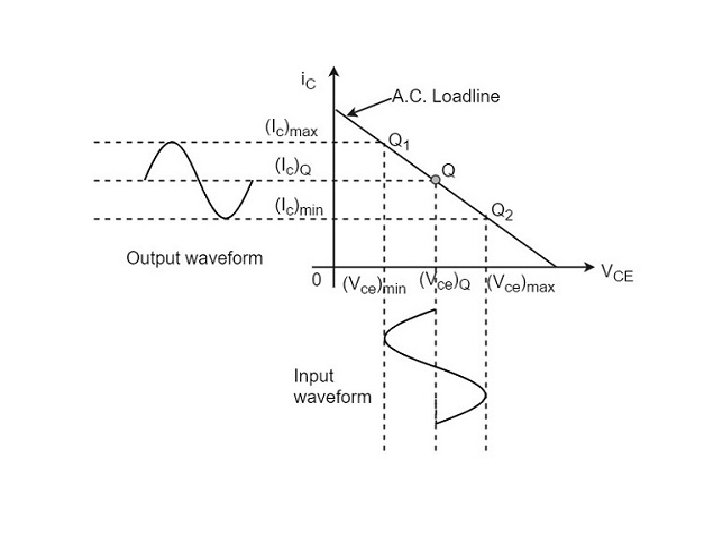
Class A Power Amplifiers • A Class A power amplifier is one in which the output current flows for the entire cycle of the AC input supply. Hence the complete signal present at the input is amplified at the output.
The operating point of this amplifier is present in the linear region. It is so selected that the current flows for the entire ac input cycle. The below figure explains the selection of operating point. The output characteristics with operating point Q is shown in the figure above. Here (Ic)Q and (Vce)Q represent no signal collector current and voltage between collector and emitter respectively. When signal is applied, the Q-point shifts to Q 1 and Q 2. The output current increases to (Ic)max and decreases to (Ic)min. Similarly, the collector-emitter voltage increases to (Vce)max and decreases to (Vce)min.
Advantages of Class A Amplifiers • The current flows for complete input cycle • It can amplify small signals • The output is same as input • No distortion is present Disadvantages of Class A Amplifiers • Low power output • Low collector efficiency
Class B Power Amplifier • When the collector current flows only during the positive half cycle of the input signal, the power amplifier is known as class B power amplifier.
Class B Operation • The biasing of the transistor in class B operation is in such a way that at zero signal condition, there will be no collector current. The operating point is selected to be at collector cut off voltage. So, when the signal is applied, only the positive half cycle is amplified at the output.
The figure below shows the input and output waveforms during class B operation.
• When the signal is applied, the circuit is forward biased for the positive half cycle of the input and hence the collector current flows. But during the negative half cycle of the input, the circuit is reverse biased and the collector current will be absent. Hence only the positive half cycle is amplified at the output. • As the negative half cycle is completely absent, the signal distortion will be high. Also, when the applied signal increases, the power dissipation will be more. But when compared to class A power amplifier, the output efficiency is increased. • Well, in order to minimize the disadvantages and achieve low distortion, high efficiency and high output power, the push-pull configuration is used in this class B amplifier.
Class C Power Amplifier • When the collector current flows for less than half cycle of the input signal, the power amplifier is known as class C power amplifier. • The efficiency of class C amplifier is high while linearity is poor. The conduction angle for class C is less than 180 o. It is generally around 90 o, which means the transistor remains idle for more than half of the input signal. So, the output current will be delivered for less time compared to the application of input signal.
The following figure shows the operating point and output of a class C amplifier
Class AB Power Amplifier As the name implies, class AB is a combination of class A and class B type of amplifiers. As class A has the problem of low efficiency and class B has distortion problem, this class AB is emerged to eliminate these two problems, by utilizing the advantages of both the classes.
Class B Push-Pull Amplifier Though the efficiency of class B power amplifier is higher than class A, as only one half cycle of the input is used, the distortion is high. Also, the input power is not completely utilized. In order to compensate these problems, the push-pull configuration is introduced in class B amplifier. Construction The circuit of a push-pull class B power amplifier consists of two identical transistors T 1 and T 2 whose bases are connected to the secondary of the center-tapped input transformer Tr 1. The emitters are shorted and the collectors are given the VCC supply through the primary of the output transformer Tr 2.
The circuit arrangement of class B push-pull amplifier, is same as that of class A push-pull amplifier except that the transistors are biased at cut off, instead of using the biasing resistors. The figure below gives the detailing of the construction of a push-pull class B power amplifier.
Operation • The circuit of class B push-pull amplifier shown in the above figure clears that both the transformers are center-tapped. When no signal is applied at the input, the transistors T 1 and T 2 are in cut off condition and hence no collector currents flow. As no current is drawn from VCC, no power is wasted. • When input signal is given, it is applied to the input transformer Tr 1 which splits the signal into two signals that are 180 o out of phase with each other. These two signals are given to the two identical transistors T 1 and T 2. For the positive half cycle, the base of the transistor T 1 becomes positive and collector current flows. At the same time, the transistor T 2 has negative half cycle, which throws the transistor T 2 into cutoff condition and hence no collector current flows.
Advantages: • High a. c. output is obtained. • The output is free from even harmonics. • The effect of ripple voltages are balanced out. These are present in the power supply due to inadequate filtering. Disadvantages: • The transistors are to be identical, to produce equal amplification. • Center-tapping is required for the transformers. • The transformers are bulky and costly.
Complementary Symmetry Push-Pull Class B Amplifier The push pull amplifier which was just discussed improves efficiency but the usage of center-tapped transformers makes the circuit bulky, heavy and costly. To make the circuit simple and to improve the efficiency, the transistors used can be complemented, as shown in the following circuit diagram.
• The above circuit employs a NPN transistor and a PNP transistor connected in push pull configuration. When the input signal is applied, during the positive half cycle of the input signal, the NPN transistor conducts and the PNP transistor cuts off. During the negative half cycle, the NPN transistor cuts off and the PNP transistor conducts. • In this way, the NPN transistor amplifies during positive half cycle of the input, while PNP transistor amplifies during negative half cycle of the input. As the transistors are both complement to each other, yet act symmetrically while being connected in push pull configuration of class B, this circuit is termed as Complementary symmetry push pull class B amplifier.
Advantages: • As there is no need of center tapped transformers, the weight and cost are reduced. • Equal and opposite input signal voltages are not required. Disadvantages: • It is difficult to get a pair of transistors (NPN and PNP) that have similar characteristics. • We require both positive and negative supply voltages.
UNIT-3 Feedback in Amplifiers
Feedback • The process of injecting a fraction of output energy of some device back to the input is known as Feedback. It has been found that feedback is very useful in reducing noise and making the amplifier operation stable.
Types of Feedbacks Positive Feedback • The feedback in which the feedback energy i. e. , either voltage or current is in phase with the input signal and thus aids it is called as Positive feedback. • Both the input signal and feedback signal introduces a phase shift of 180 o thus making a 360 o resultant phase shift around the loop, to be finally in phase with the input signal.
Negative Feedback • The feedback in which the feedback energy i. e. , either voltage or current is out of phase with the input and thus opposes it, is called as negative feedback. • In negative feedback, the amplifier introduces a phase shift of 180 o into the circuit while the feedback network is so designed that it produces no phase shift or zero phase shift. Thus the resultant feedback voltage Vf is 180 o out of phase with the input signal Vin.
Principle of Feedback Amplifier A feedback amplifier generally consists of two parts. They are the amplifier and the feedback circuit. The feedback circuit usually consists of resistors. The concept of feedback amplifier can be understood from the following figure.
• From the above figure, the gain of the amplifier is represented as A. the gain of the amplifier is the ratio of output voltage Vo to the input voltage Vi. the feedback network extracts a voltage Vf= β Vo from the output Vo of the amplifier. • This voltage is added for positive feedback and subtracted for negative feedback, from the signal voltage Vs. Now, • Vi=Vs+Vf=Vs+βVo • Vi=Vs−Vf=Vs−βVo • The quantity β = Vf/Vo is called as feedback ratio or feedback fraction.
• Let us consider the case of negative feedback. The output Vomust be equal to the input voltage (Vs - βVo) multiplied by the gain A of the amplifier. • Hence, • (Vs−βVo)A=Vo • Or • AVs−AβVo=Vo • Or • AVs=Vo(1+Aβ) • Therefore, • Vo/Vs=A/1+Aβ
• Let Af be the overall gain (gain with the feedback) of the amplifier. This is defined as the ratio of output voltage Vo to the applied signal voltage Vs, i. e. , • Af=Outputvoltage/Inputsignalvoltage=Vo/Vs • So, from the above two equations, we can understand that, • The equation of gain of the feedback amplifier, with negative feedback is given by • Af=A/1+Aβ • The equation of gain of the feedback amplifier, with positive feedback is given by • Af=A/1−Aβ • These are the standard equations to calculate the gain of feedback amplifiers.
Amplifiers Negative Feedback There are two main types of negative feedback circuits. They are − I. Negative Voltage Feedback II. Negative Current Feedback Negative Voltage Feedback In this method, the voltage feedback to the input of amplifier is proportional to the output voltage. • Voltage-series feedback • Voltage-shunt feedback Negative Current Feedback In this method, the voltage feedback to the input of amplifier is proportional to the output current. • Current-series feedback • Current-shunt feedback
Voltage-Series Feedback Voltage-Shunt Feedback
Current-Series Feedback Current-Shunt Feedback
Advantages of negative feedback • • Stability of gain is improved Reduction in distortion Reduction in noise Increase in input impedance Decrease in output impedance Improve Bandwidth or Frequency response Increase in the range of uniform application
Emitter Follower Emitter follower is a case of negative current feedback circuit. This is mostly used as a last stage amplifier in signal generator circuits. The important features of Emitter Follower are − • It has high input impedance • It has low output impedance • It is ideal circuit for impedance matching All these ideal features allow many applications for the emitter follower circuit. This is a current amplifier circuit that has no voltage gain.
Construction • The constructional details of an emitter follower circuit are nearly similar to a normal amplifier. The main difference is that the load RL is absent at the collector terminal, but present at the emitter terminal of the circuit. Thus the output is taken from the emitter terminal instead of collector terminal. • The biasing is provided either by base resistor method or by potential divider method.
The following figure shows the circuit diagram of an Emitter Follower
Operation The input signal voltage applied between base and emitter, develops an output voltage Vo across RE, which is in the emitter section. Therefore, • Vo=IERE • The whole of this output current is applied to the input through feedback. Hence, • Vf=Vo • As the output voltage developed across RL is proportional to the emitter current, this emitter follower circuit is a current feedback circuit. Hence, • β=Vf/Vo=1 • It is also noted that the input signal voltage to the transistor (= Vi) is equal to the difference of Vs and Vo i. e. , • Vi=Vs−Vo Hence the feedback is negative.
Characteristics • • No voltage gain. In fact, the voltage gain is nearly 1. Relatively high current gain and power gain. High input impedance and low output impedance. Input and output ac voltages are in phase.
UNIT-4 Sinusoidal Oscillators
Sinusoidal Oscillators • An oscillator generates output without any ac input signal. • An electronic oscillator is a circuit which converts dc energy into ac at a very high frequency. • An amplifier with a positive feedback can be understood as an oscillator.
Alternator vs. Oscillator • An alternator converts mechanical energy to a. c. energy, whereas the oscillator converts d. c. energy into a. c. energy. • An oscillator can produce higher frequencies of several MHz whereas an alternator cannot. • An alternator has rotating parts, whereas an electronic oscillator doesn’t. • It is easy to change the frequency of oscillations in an oscillator than in an alternator.
Nature of Sinusoidal Oscillations Damped Oscillations • The electrical oscillations whose amplitude goes on decreasing with time are called as Damped Oscillations. The frequency of the damped oscillations may remain constant depending upon the circuit parameters.
Undamped Oscillations • The electrical oscillations whose amplitude remains constant with time are called as Undamped Oscillations. The frequency of the Undamped oscillations remains constant.
The Oscillatory Circuit • An oscillatory circuit produces electrical oscillations of a desired frequency. They are also known as tank circuits. • A simple tank circuit comprises of an inductor L and a capacitor C both of which together determine the oscillatory frequency of the circuit. • To understand the concept of oscillatory circuit, let us consider the following circuit. The capacitor in this circuit is already charged using a dc source. In this situation, the upper plate of the capacitor has excess of electrons whereas the lower plate has deficit of electrons. The capacitor holds some electrostatic energy and there is a voltage across the capacitor.
When the switch S is closed, the capacitor discharges and the current flows through the inductor. Due to the inductive effect, the current builds up slowly towards a maximum value. Once the capacitor discharges completely, the magnetic field around the coil is maximum.
Now, let us move on to the next stage. Once the capacitor is discharged completely, the magnetic field begins to collapse and produces a counter EMF according to Lenz’s law. The capacitor is now charged with positive charge on the upper plate and negative charge on the lower plate. Once the capacitor is fully charged, it starts to discharge to build up a magnetic field around the coil, as shown in the following circuit diagram.
• This continuation of charging and discharging results in alternating motion of electrons or an oscillatory current. The interchange of energy between L and C produce continuous oscillations. • In an ideal circuit, where there are no losses, the oscillations would continue indefinitely. In a practical tank circuit, there occur losses such as resistive and radiation losses in the coil and dielectric losses in the capacitor. These losses result in damped oscillations.
Practical Oscillator Circuit • Tank Circuit − The tank circuit consists of an inductance L connected in parallel with capacitor C. The values of these two components determine the frequency of the oscillator circuit. • Transistor Amplifier − The output of the tank circuit is connected to the amplifier circuit so that the oscillations produced by the tank circuit are amplified here. Hence the output of these oscillations are increased by the amplifier. • Feedback Circuit − The function of feedback circuit is to transfer a part of the output energy to LC circuit in proper phase. This feedback is positive in oscillators while negative in amplifiers.
Principle of Feedback Amplifier A feedback amplifier generally consists of two parts. They are the amplifier and the feedback circuit. The feedback circuit usually consists of resistors. The concept of feedback amplifier can be understood from the following figure below. From the above figure, the gain of the amplifier is represented as A.
• The gain of the amplifier is the ratio of output voltage Vo to the input voltage Vi. The feedback network extracts a voltage Vf= β Vo from the output Vo of the amplifier. • This voltage is added for positive feedback and subtracted for negative feedback, from the signal voltage Vs. • So, for a positive feedback, • Vi = Vs + Vf = Vs + β Vo • The quantity β = Vf/Vo is called as feedback ratio or feedback fraction. • The output Vo must be equal to the input voltage (Vs + βVo) multiplied by the gain A of the amplifier. Hence, • (Vs+βVo)A=Vo Or • AVs+AβVo=Vo Or • AVs=Vo(1−Aβ) • Therefore , Vo/Vs=A/1−Aβ
• Let Af be the overall gain (gain with the feedback) of the amplifier. This is defined as the ratio of output voltage Vo to the applied signal voltage Vs, i. e. , • Af=Output. Voltage/Input. Signal. Voltage=Vo/Vs • From the above two equations, we can understand that, the equation of gain of the feedback amplifier with positive feedback is given by • Af=A/1−Aβ • Where Aβ is the feedback factor or the loop gain. • If Aβ = 1, Af = ∞. Thus the gain becomes infinity, i. e. , there is output without any input. In another words, the amplifier works as an Oscillator. • The condition Aβ = 1 is called as Barkhausen Criterion of oscillations. This is a very important factor to be always kept in mind, in the concept of Oscillators.
Tuned Collector Oscillator Tuned collector oscillators are called so, because the tuned circuit is placed in the collector of the transistor amplifier. The combination of L and C form the tuned circuit or frequency determining circuit. Construction The resistors R 1, R 2 and RE are used to provide d. c. bias to the transistor. The capacitors CE and C are the by-pass capacitors. The secondary of the transformer provides a. c. feedback voltage that appears across the base-emitter junction of R 1 and R 2 is at a. c. ground due to by-pass capacitor C. In case, the capacitor was absent, a part of the voltage induced in the secondary of the transformer would drop across R 2 instead of completely going to the input of transistor.
As the CE configured transistor provides 180 o phase shift, another 180 o phase shift is provided by the transformer, which makes 360 o phase shift between the input and output voltages. The following circuit diagram shows the arrangement of a tuned collector circuit.
Operation • Once the supply is given, the collector current starts increasing and charging of capacitor C takes place. When the capacitor is fully charged, it discharges through the inductance L 1. Now oscillations are produced. These oscillations induce some voltage in the secondary winding L 2. The frequency of voltage induced in the secondary winding is same as that of the tank circuit and its magnitude depends upon the number of turns in secondary winding and coupling between both the windings. • The voltage across L 2 is applied between base and emitter and appears in the amplified form in the collector circuit, thus overcoming the losses in the tank circuit. The number of turns of L 2 and coupling between L 1 and L 2 are so adjusted that oscillations across L 2 are amplified to a level just sufficient to supply losses to the tank circuit. • Tuned collector oscillators are widely used as the local oscillator in radio receivers.
Hartley Oscillator A very popular local oscillator circuit that is mostly used in radio receivers is the Hartley Oscillator circuit. Construction • In the circuit diagram of a Hartley oscillator shown below, the resistors R 1, R 2 and Re provide necessary bias condition for the circuit. The capacitor Ce provides a. c. ground thereby providing any signal degeneration. This also provides temperature stabilization. • The capacitors Cc and Cb are employed to block d. c. and to provide an a. c. path. The radio frequency choke (R. F. C) offers very high impedance to high frequency currents which means it shorts for d. c. and opens for a. c. Hence it provides d. c. load for collector and keeps a. c. currents out of d. c. supply source
Tank Circuit • The frequency determining network is a parallel resonant circuit which consists of the inductors L 1 and L 2 along with a variable capacitor C. The junction of L 1 and L 2 are earthed. The coil L 1 has its one end connected to base via Cc and the other to emitter via Ce. So, L 2 is in the output circuit. Both the coils L 1 and L 2 are inductively coupled and together form an Autotransformer.
The following circuit diagram shows the arrangement of a Hartley oscillator. The tank circuit is shunt fed in this circuit. It can also be a series-fed.
Operation • When the collector supply is given, a transient current is produced in the oscillatory or tank circuit. The oscillatory current in the tank circuit produces a. c. voltage across L 1. • The auto-transformer made by the inductive coupling of L 1 and L 2 helps in determining the frequency and establishes the feedback. As the CE configured transistor provides 180 o phase shift, another 180 o phase shift is provided by the transformer, which makes 360 o phase shift between the input and output voltages. • This makes the feedback positive which is essential for the condition of oscillations. When the loop gain |βA| of the amplifier is greater than one, oscillations are sustained in the circuit.
Operation Frequency • The equation for frequency of Hartley oscillator is given as • f=1/√ 2πLTC • LT=L 1+L 2+2 M • Here, LT is the total cumulatively coupled inductance; L 1 and L 2 represent inductances of 1 st and 2 nd coils; and M represents mutual inductance. • Mutual inductance is calculated when two windings are considered.
Advantages: • Instead of using a large transformer, a single coil can be used as an auto-transformer. • Frequency can be varied by employing either a variable capacitor or a variable inductor. • Less number of components are sufficient. • The amplitude of the output remains constant over a fixed frequency range. Disadvantages: • It cannot be a low frequency oscillator. • Harmonic distortions are present. • Applications • The applications of Hartley oscillator are • It is used to produce a sine wave of desired frequency. • Mostly used as a local oscillator in radio receivers. • It is also used as R. F. Oscillator.
Colpitts Oscillator A Colpitts oscillator looks just like the Hartley oscillator but the inductors and capacitors are replaced with each other in the tank circuit.
Frequency of Colpitts oscillator • The equation for frequency of Colpitts oscillator is given as • f=1√ 2πLCT • CT is the total capacitance of C 1 and C 2 connected in series. • 1/CT=1/C 1+1/C 2 • CT=C 1×C 2 / C 1+C 2
Advantages • Colpitts oscillator can generate sinusoidal signals of very high frequencies. • It can withstand high and low temperatures. • The frequency stability is high. • Frequency can be varied by using both the variable capacitors. • Less number of components are sufficient. • The amplitude of the output remains constant over a fixed frequency range. Applications • Colpitts oscillator can be used as High frequency sine wave generator. • This can be used as a temperature sensor with some associated circuitry. • Mostly used as a local oscillator in radio receivers. • It is also used as R. F. Oscillator. • It is also used in Mobile applications. • It has got many other commercial applications.
Phase Shift Oscillators The oscillator circuit that produces a sine wave using a phaseshift network is called as a Phase-shift oscillator circuit. Construction • The phase-shift oscillator circuit consists of a single transistor amplifier section and a RC phase-shift network. The phase shift network in this circuit, consists of three RC sections. At the resonant frequency fo, the phase shift in each RC section is 60 oso that the total phase shift produced by RC network is 180 o.
Circuit diagram of an RC phase-shift oscillator • • The frequency of oscillations is given by fo=1/2πRC√ 6 Where R 1=R 2=R 3=R & C 1=C 2=C 3=C
Operation • The circuit when switched ON oscillates at the resonant frequency fo. The output Eo of the amplifier is fed back to RC feedback network. This network produces a phase shift of 180 oand a voltage Ei appears at its output. This voltage is applied to the transistor amplifier. • The feedback applied will be m = Ei/Eo • The feedback is in correct phase, whereas the transistor amplifier, which is in CE configuration, produces a 180 o phase shift. The phase shift produced by network and the transistor add to form a phase shift around the entire loop which is 360 o.
Advantages • It does not require transformers or inductors. • It can be used to produce very low frequencies. • The circuit provides good frequency stability. Disadvantages • Starting the oscillations is difficult as the feedback is small. • The output produced is small.
Wien Bridge Oscillator • Wien bridge oscillator circuit is mostly used because of its important features. This circuit is free from the circuit fluctuations and the ambient temperature. • The main advantage of this oscillator is that the frequency can be varied in the range of 10 Hz to about 1 MHz whereas in RC oscillators, the frequency is not varied. Construction • The circuit construction of Wien bridge oscillator can be explained as below. It is a two-stage amplifier with RC bridge circuit. The bridge circuit has the arms R 1 C 1, R 3, R 2 C 2 and the tungsten lamp Lp. Resistance R 3 and the lamp Lp are used to stabilize the amplitude of the output.
Circuit diagram a Wien bridge oscillator The transistor T 1 serves as an oscillator and an amplifier while the other transistor T 2 serves as an inverter. The inverter operation provides a phase shift of 180 o. This circuit provides positive feedback through R 1 C 1, C 2 R 2 to the transistor T 1 and negative feedback through the voltage divider to the input of transistor T 2.
Operation • When the circuit is switched ON, the bridge circuit produces oscillations of the frequency stated above. The two transistors produce a total phase shift of 360 o so that proper positive feedback is ensured. The negative feedback in the circuit ensures constant output. This is achieved by temperature sensitive tungsten lamp Lp. Its resistance increases with current. • If the amplitude of the output increases, more current is produced and more negative feedback is achieved. Due to this, the output would return to the original value. Whereas, if the output tends to decrease, reverse action would take place. • Frequency f=1/2π√R 1 C 1 R 2 C 2 If R 1 = R 2 and C 1 = C 2 = C Then, f=1/2πRC
Advantages • The circuit provides good frequency stability. • It provides constant output. • The operation of circuit is quite easy. • The overall gain is high because of two transistors. • The frequency of oscillations can be changed easily. • The amplitude stability of the output voltage can be maintained more accurately, by replacing R 2 with a thermistor. Disadvantages • The circuit cannot generate very high frequencies. • Two transistors and number of components are required for the circuit construction.
Crystal Oscillators • The principle of crystal oscillators depends upon the Piezo electric effect. The natural shape of a crystal is hexagonal. When a crystal wafer is cur perpendicular to X-axis, it is called as X-cut and when it is cut along Y-axis, it is called as Y-cut. • The crystal used in crystal oscillator exhibits a property called as Piezo electric property. Piezo Electric Effect • The crystal exhibits the property that when a mechanical stress is applied across one of the faces of the crystal, a potential difference is developed across the opposite faces of the crystal. Conversely, when a potential difference is applied across one of the faces, a mechanical stress is produced along the other faces.
Crystal Oscillator Circuit • A crystal oscillator circuit can be constructed in a number of ways like a Crystal controlled tuned collector oscillator, a Colpitts crystal oscillator, a Clap crystal oscillator etc. But the transistor pierce crystal oscillator is the most commonly used one. This is the circuit which is normally referred as a crystal oscillator circuit.
circuit diagram crystal oscillator • In this circuit, the crystal is connected as a series element in the feedback path from collector to the base. The resistors R 1, R 2 and RE provide a voltage-divider stabilized d. c. bias circuit. The capacitor CE provides a. c. bypass of the emitter resistor and RFC (radio frequency choke) coil provides for d. c. bias while decoupling any a. c. signal on the power lines from affecting the output signal. The coupling capacitor C has negligible impedance at the circuit operating frequency. But it blocks any d. c. between collector and base.
• The circuit frequency of oscillation is set by the series resonant frequency of the crystal and its value is given by the relation, fo=1/√ 2πL. C
Advantages • They have a high order of frequency stability. • The quality factor (Q) of the crystal is very high. Disadvantages • They are fragile and can be used in low power circuits. • The frequency of oscillations cannot be changed appreciably.