Introduction to CMOS VLSI Design SRAM 1 Outline

- Slides: 38

Introduction to CMOS VLSI Design SRAM 1

Outline q Memory Arrays q SRAM Architecture – SRAM Cell – Decoders – Column Circuitry – Multiple Ports q Serial Access Memories SRAM CMOS VLSI Design 2

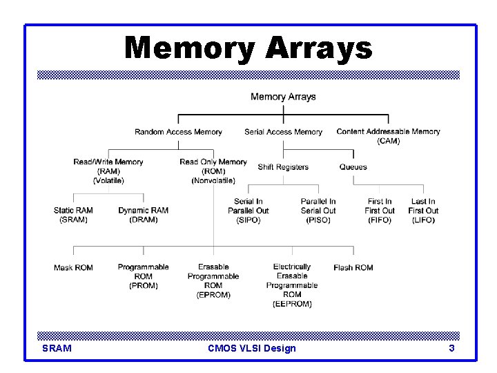
Memory Arrays SRAM CMOS VLSI Design 3

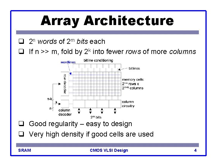
Array Architecture q 2 n words of 2 m bits each q If n >> m, fold by 2 k into fewer rows of more columns q Good regularity – easy to design q Very high density if good cells are used SRAM CMOS VLSI Design 4

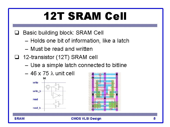
12 T SRAM Cell q Basic building block: SRAM Cell – Holds one bit of information, like a latch – Must be read and written q 12 -transistor (12 T) SRAM cell – Use a simple latch connected to bitline – 46 x 75 l unit cell SRAM CMOS VLSI Design 5

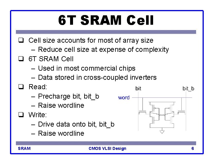
6 T SRAM Cell q Cell size accounts for most of array size – Reduce cell size at expense of complexity q 6 T SRAM Cell – Used in most commercial chips – Data stored in cross-coupled inverters q Read: – Precharge bit, bit_b – Raise wordline q Write: – Drive data onto bit, bit_b – Raise wordline SRAM CMOS VLSI Design 6

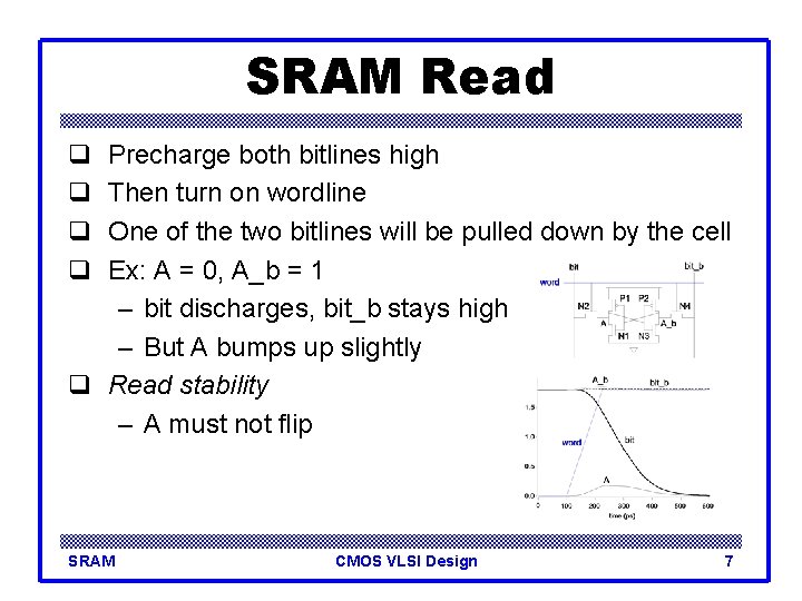
SRAM Read q q Precharge both bitlines high Then turn on wordline One of the two bitlines will be pulled down by the cell Ex: A = 0, A_b = 1 – bit discharges, bit_b stays high – But A bumps up slightly q Read stability – A must not flip SRAM CMOS VLSI Design 7

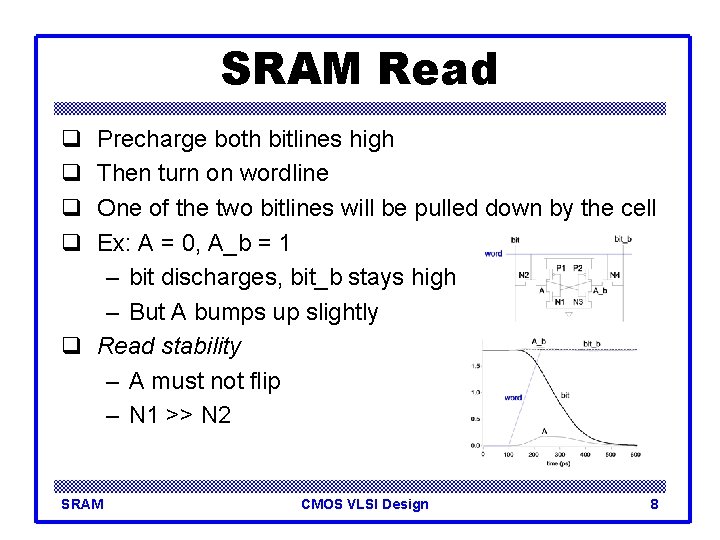
SRAM Read q q Precharge both bitlines high Then turn on wordline One of the two bitlines will be pulled down by the cell Ex: A = 0, A_b = 1 – bit discharges, bit_b stays high – But A bumps up slightly q Read stability – A must not flip – N 1 >> N 2 SRAM CMOS VLSI Design 8

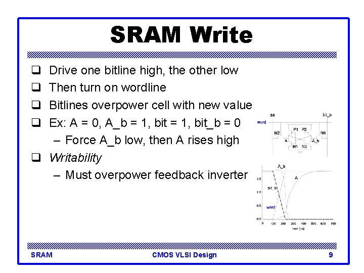
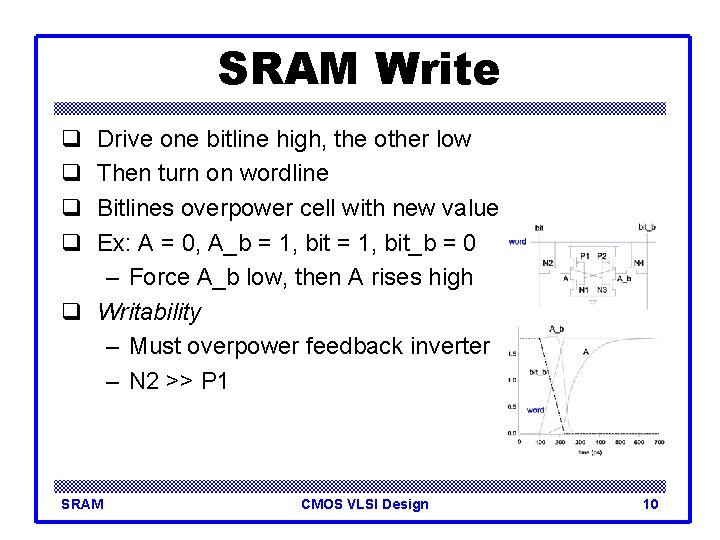
SRAM Write q q Drive one bitline high, the other low Then turn on wordline Bitlines overpower cell with new value Ex: A = 0, A_b = 1, bit_b = 0 – Force A_b low, then A rises high q Writability – Must overpower feedback inverter SRAM CMOS VLSI Design 9

SRAM Write q q Drive one bitline high, the other low Then turn on wordline Bitlines overpower cell with new value Ex: A = 0, A_b = 1, bit_b = 0 – Force A_b low, then A rises high q Writability – Must overpower feedback inverter – N 2 >> P 1 SRAM CMOS VLSI Design 10

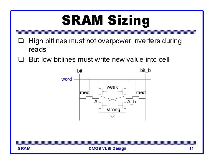
SRAM Sizing q High bitlines must not overpower inverters during reads q But low bitlines must write new value into cell SRAM CMOS VLSI Design 11

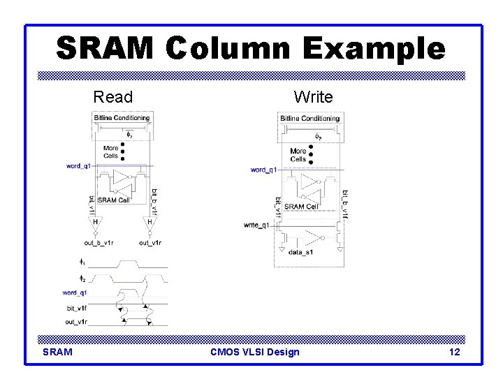
SRAM Column Example Read SRAM Write CMOS VLSI Design 12

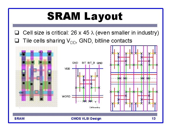
SRAM Layout q Cell size is critical: 26 x 45 l (even smaller in industry) q Tile cells sharing VDD, GND, bitline contacts SRAM CMOS VLSI Design 13

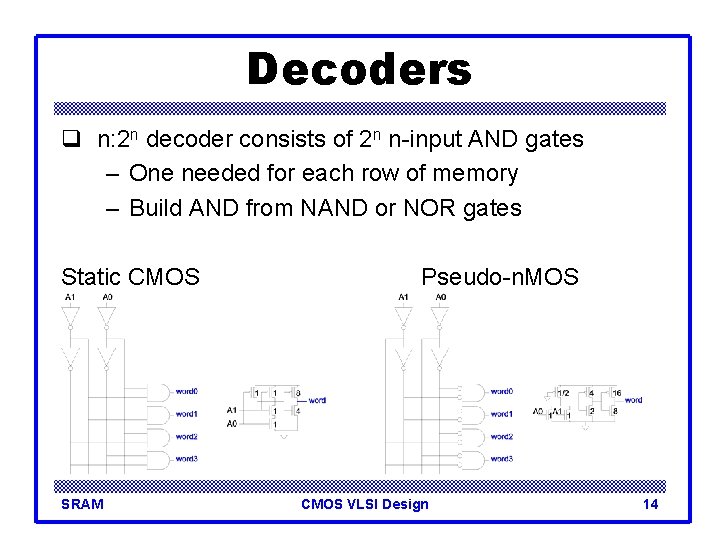
Decoders q n: 2 n decoder consists of 2 n n-input AND gates – One needed for each row of memory – Build AND from NAND or NOR gates Static CMOS SRAM Pseudo-n. MOS CMOS VLSI Design 14

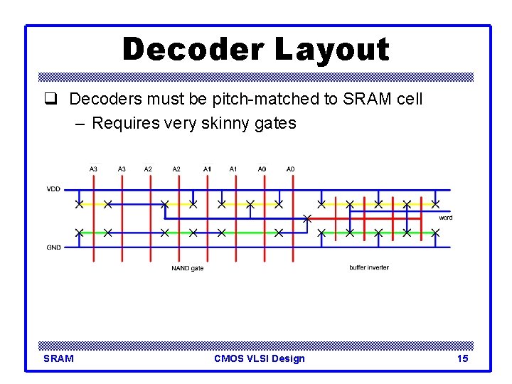
Decoder Layout q Decoders must be pitch-matched to SRAM cell – Requires very skinny gates SRAM CMOS VLSI Design 15

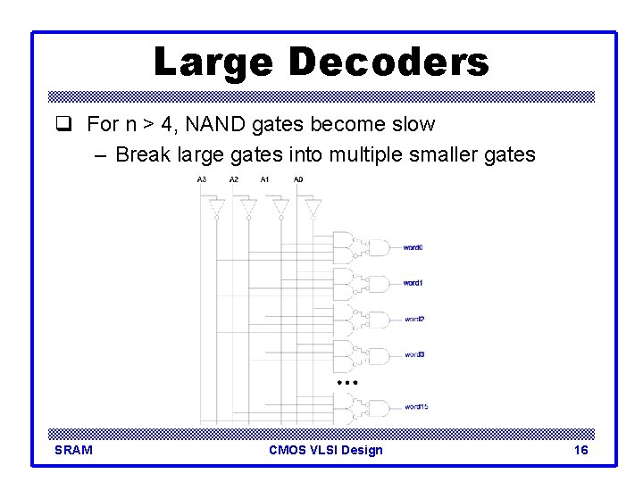
Large Decoders q For n > 4, NAND gates become slow – Break large gates into multiple smaller gates SRAM CMOS VLSI Design 16

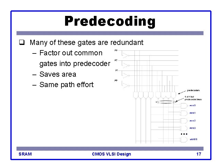
Predecoding q Many of these gates are redundant – Factor out common gates into predecoder – Saves area – Same path effort SRAM CMOS VLSI Design 17

Column Circuitry q Some circuitry is required for each column – Bitline conditioning – Sense amplifiers – Column multiplexing SRAM CMOS VLSI Design 18

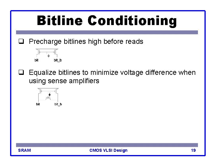
Bitline Conditioning q Precharge bitlines high before reads q Equalize bitlines to minimize voltage difference when using sense amplifiers SRAM CMOS VLSI Design 19

Sense Amplifiers q Bitlines have many cells attached – Ex: 32 -kbit SRAM has 256 rows x 128 cols – 128 cells on each bitline q tpd (C/I) DV – Even with shared diffusion contacts, 64 C of diffusion capacitance (big C) – Discharged slowly through small transistors (small I) q Sense amplifiers are triggered on small voltage swing (reduce DV) SRAM CMOS VLSI Design 20

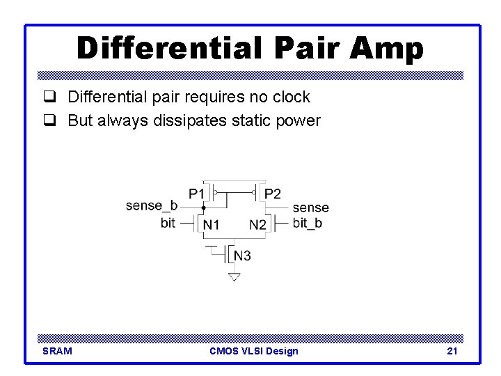
Differential Pair Amp q Differential pair requires no clock q But always dissipates static power SRAM CMOS VLSI Design 21

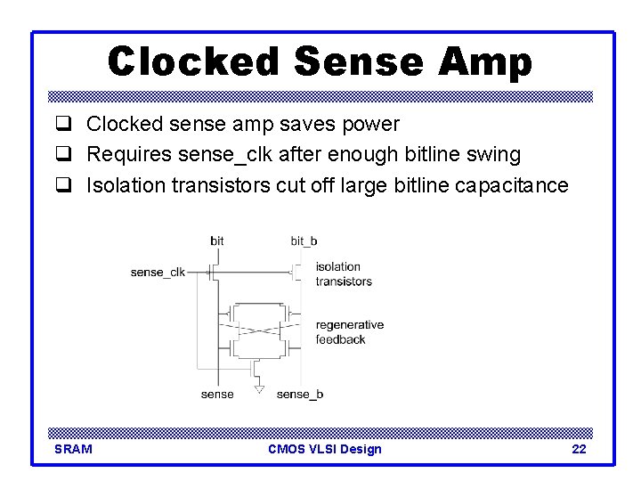
Clocked Sense Amp q Clocked sense amp saves power q Requires sense_clk after enough bitline swing q Isolation transistors cut off large bitline capacitance SRAM CMOS VLSI Design 22

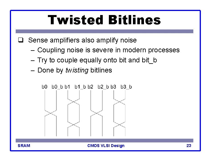
Twisted Bitlines q Sense amplifiers also amplify noise – Coupling noise is severe in modern processes – Try to couple equally onto bit and bit_b – Done by twisting bitlines SRAM CMOS VLSI Design 23

Column Multiplexing q Recall that array may be folded for good aspect ratio q Ex: 2 kword x 16 folded into 256 rows x 128 columns – Must select 16 output bits from the 128 columns – Requires 16 8: 1 column multiplexers SRAM CMOS VLSI Design 24

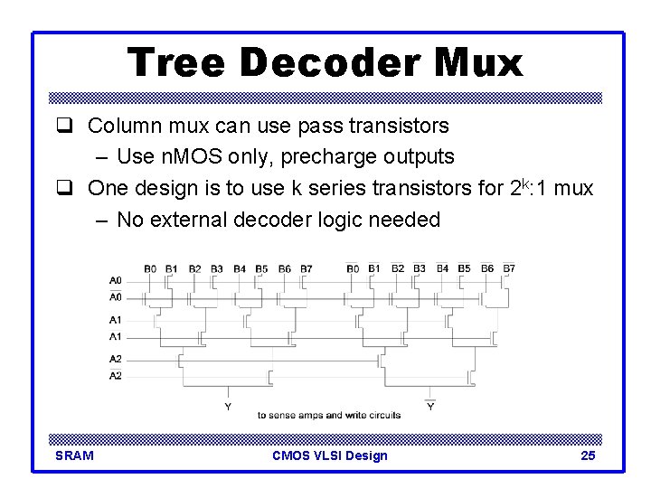
Tree Decoder Mux q Column mux can use pass transistors – Use n. MOS only, precharge outputs q One design is to use k series transistors for 2 k: 1 mux – No external decoder logic needed SRAM CMOS VLSI Design 25

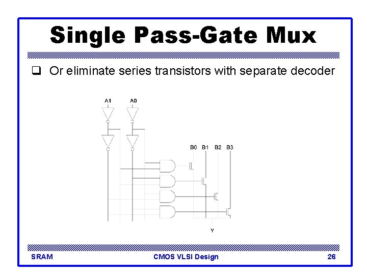
Single Pass-Gate Mux q Or eliminate series transistors with separate decoder SRAM CMOS VLSI Design 26

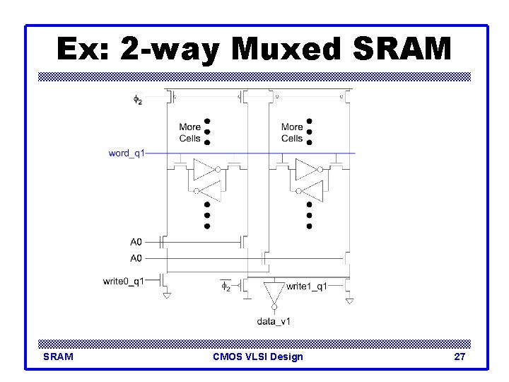
Ex: 2 -way Muxed SRAM CMOS VLSI Design 27

Multiple Ports q We have considered single-ported SRAM – One read or one write on each cycle q Multiported SRAM are needed for register files q Examples: – Multicycle MIPS must read two sources or write a result on some cycles – Pipelined MIPS must read two sources and write a third result each cycle – Superscalar MIPS must read and write many sources and results each cycle SRAM CMOS VLSI Design 28

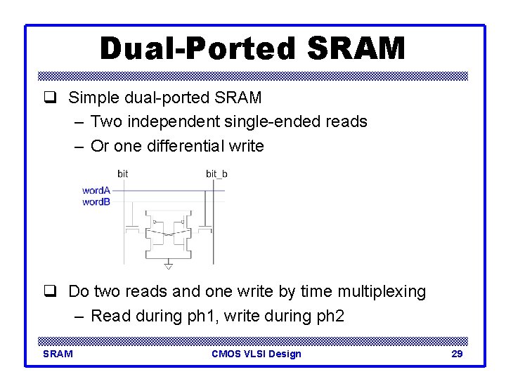
Dual-Ported SRAM q Simple dual-ported SRAM – Two independent single-ended reads – Or one differential write q Do two reads and one write by time multiplexing – Read during ph 1, write during ph 2 SRAM CMOS VLSI Design 29

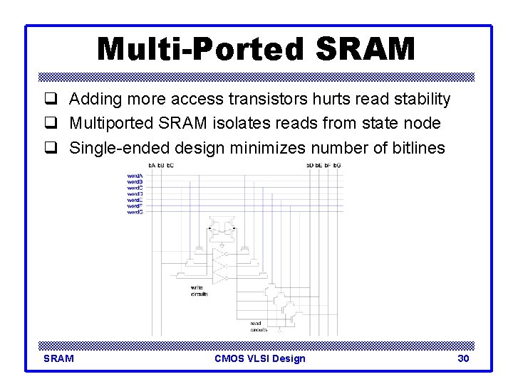
Multi-Ported SRAM q Adding more access transistors hurts read stability q Multiported SRAM isolates reads from state node q Single-ended design minimizes number of bitlines SRAM CMOS VLSI Design 30

Serial Access Memories q Serial access memories do not use an address – Shift Registers – Tapped Delay Lines – Serial In Parallel Out (SIPO) – Parallel In Serial Out (PISO) – Queues (FIFO, LIFO) SRAM CMOS VLSI Design 31

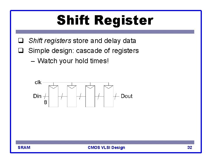
Shift Register q Shift registers store and delay data q Simple design: cascade of registers – Watch your hold times! SRAM CMOS VLSI Design 32

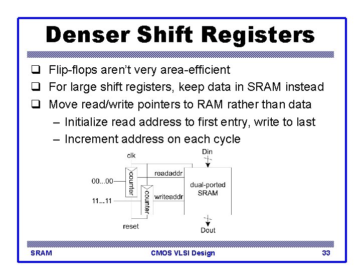
Denser Shift Registers q Flip-flops aren’t very area-efficient q For large shift registers, keep data in SRAM instead q Move read/write pointers to RAM rather than data – Initialize read address to first entry, write to last – Increment address on each cycle SRAM CMOS VLSI Design 33

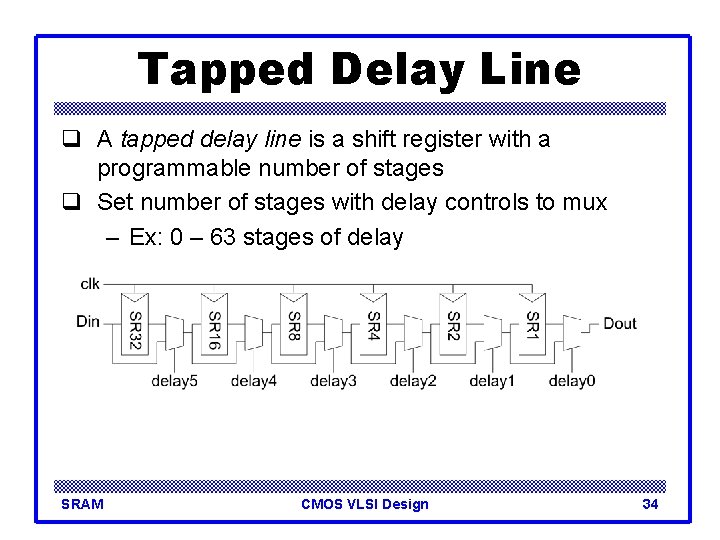
Tapped Delay Line q A tapped delay line is a shift register with a programmable number of stages q Set number of stages with delay controls to mux – Ex: 0 – 63 stages of delay SRAM CMOS VLSI Design 34

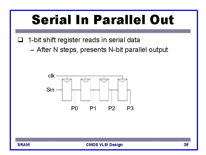
Serial In Parallel Out q 1 -bit shift register reads in serial data – After N steps, presents N-bit parallel output SRAM CMOS VLSI Design 35

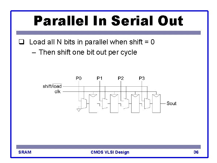
Parallel In Serial Out q Load all N bits in parallel when shift = 0 – Then shift one bit out per cycle SRAM CMOS VLSI Design 36

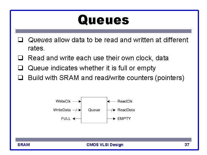
Queues q Queues allow data to be read and written at different rates. q Read and write each use their own clock, data q Queue indicates whether it is full or empty q Build with SRAM and read/write counters (pointers) SRAM CMOS VLSI Design 37

FIFO, LIFO Queues q First In First Out (FIFO) – Initialize read and write pointers to first element – Queue is EMPTY – On write, increment write pointer – If write almost catches read, Queue is FULL – On read, increment read pointer q Last In First Out (LIFO) – Also called a stack – Use a single stack pointer for read and write SRAM CMOS VLSI Design 38