CPE 626 Advanced VLSI Design Aleksandar Milenkovic http



- Slides: 27

CPE 626 Advanced VLSI Design Aleksandar Milenkovic http: //www. ece. uah. edu/~milenka/cpe 626 -04 F/ milenka@ece. uah. edu Assistant Professor Electrical and Computer Engineering Dept. University of Alabama in Huntsville

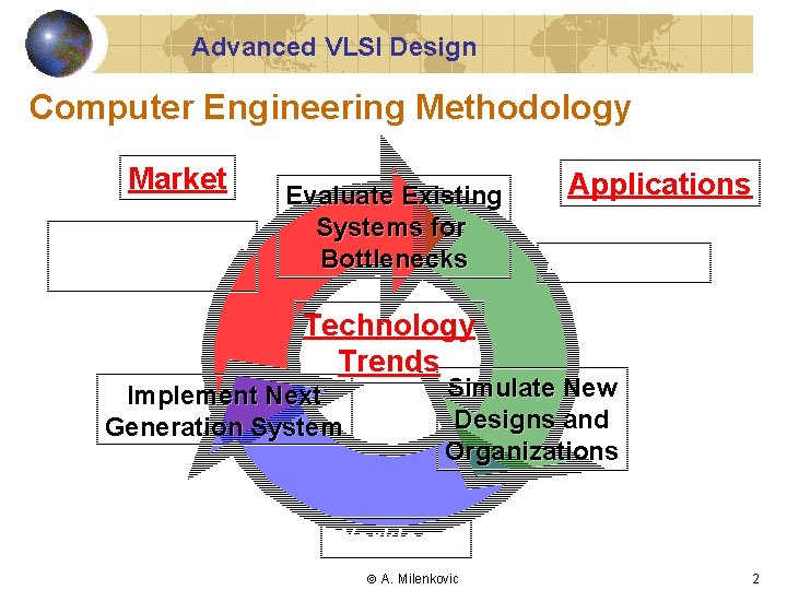
Advanced VLSI Design Computer Engineering Methodology Market Implementation Complexity Evaluate Existing Systems for Bottlenecks Applications Benchmarks Technology Trends Implement Next Generation System Simulate New Designs and Organizations Workloads A. Milenkovic 2

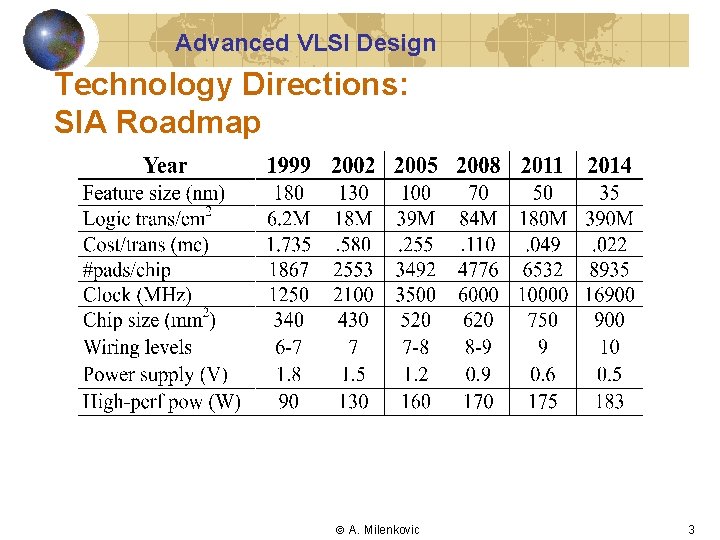
Advanced VLSI Design Technology Directions: SIA Roadmap A. Milenkovic 3

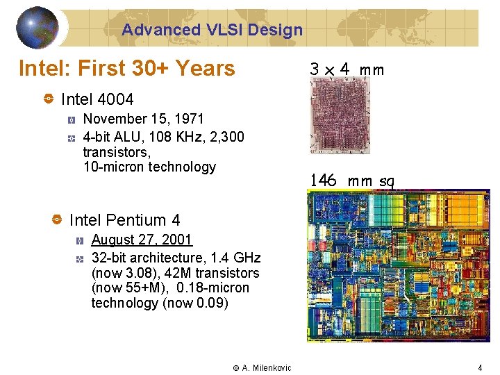
Advanced VLSI Design Intel: First 30+ Years 3 x 4 mm Intel 4004 November 15, 1971 4 -bit ALU, 108 KHz, 2, 300 transistors, 10 -micron technology 146 mm sq Intel Pentium 4 August 27, 2001 32 -bit architecture, 1. 4 GHz (now 3. 08), 42 M transistors (now 55+M), 0. 18 -micron technology (now 0. 09) A. Milenkovic 4

Advanced VLSI Design Future Applications Desktop: 90% of cycles will be spent on media applications video encode/decode, polygon & image-based graphics audio processing, compression, music, speech recognition/synthesis modulation/demodulation at audio and video rates Scientific desktops: high-performance FPs and graphics Commercial servers: support for databases and transaction processing, enhancement for reliability, support for scalability Embedded computing: special support for graphics or video, power limitations A. Milenkovic 5

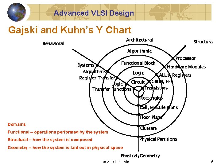
Advanced VLSI Design Gajski and Kuhn’s Y Chart Architectural Behavioral Structural Algorithmic Functional Block Systems Processor Hardware Modules Algorithms Logic ALUs, Registers Register Transfer Gates, FFs Circuit Logic Transistors Transfer Functions Rectangles Cell, Module Plans Floor Plans Domains Clusters Functional – operations performed by the system Physical Partitions Structural – how the system is composed Geometry – how the system is laid out in physical space Physical/Geometry A. Milenkovic 6

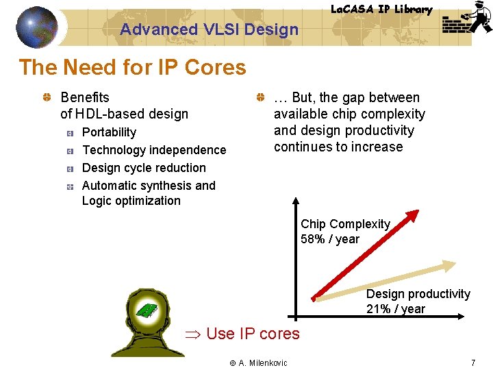
La. CASA IP Library Advanced VLSI Design The Need for IP Cores Benefits of HDL-based design Portability Technology independence Design cycle reduction Automatic synthesis and Logic optimization … But, the gap between available chip complexity and design productivity continues to increase Chip Complexity 58% / year Design productivity 21% / year Use IP cores A. Milenkovic 7

La. CASA IP Library Advanced VLSI Design New Generation of Designers … Emphasis on hierarchical IP core design Design systems, not components! Understand hardware/software co-design Understand explore design tradeoffs between complexity, performance, and power consumption Design a soft processor/micro-controller core A. Milenkovic 8

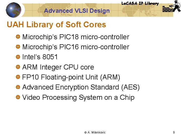
La. CASA IP Library Advanced VLSI Design UAH Library of Soft Cores Microchip’s PIC 18 micro-controller Microchip’s PIC 16 micro-controller Intel’s 8051 ARM Integer CPU core FP 10 Floating-point Unit (ARM) Advanced Encryption Standard (AES) Video Processing System on a Chip A. Milenkovic 9

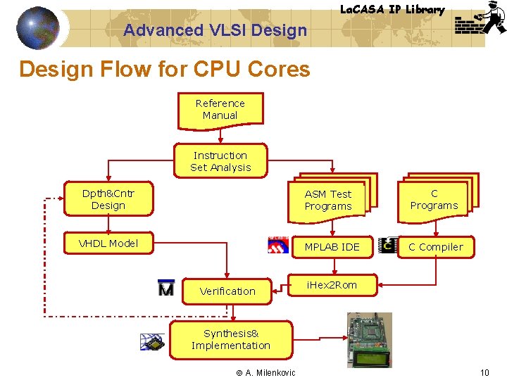
La. CASA IP Library Advanced VLSI Design Flow for CPU Cores Reference Manual Instruction Set Analysis Dpth&Cntr Design VHDL Model Verification ASM Test Programs C Programs MPLAB IDE C Compiler i. Hex 2 Rom Synthesis& Implementation A. Milenkovic 10

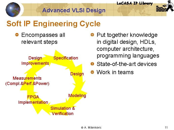
La. CASA IP Library Advanced VLSI Design Soft IP Engineering Cycle Encompasses all relevant steps Design Specification Improvements Measurements (Compl. &Perf. &Power) FPGA Implementation Design Put together knowledge in digital design, HDLs, computer architecture, programming languages State-of-the-art devices Work in teams Modeling Simulation & Verification A. Milenkovic 11

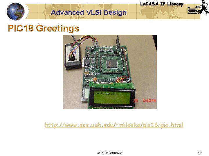
La. CASA IP Library Advanced VLSI Design PIC 18 Greetings http: //www. ece. uah. edu/~milenka/pic 18/pic. html A. Milenkovic 12

Advanced VLSI Designing a simple CPU in 60 minutes La. CASA step-by-step tutorial http: //www. ece. uah. edu/~lacasa/tutorials/mu 0 tutorial. html Design, verify, implement, and prototype a rudimentary processor MU 0 Modeling using VHDL Simulation using Model. Sim Implement using Xilinx ISE and a Spartan. II device A. Milenkovic 13

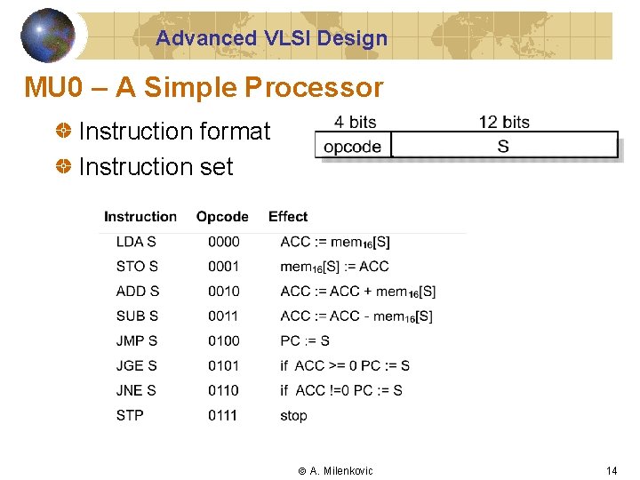
Advanced VLSI Design MU 0 – A Simple Processor Instruction format Instruction set A. Milenkovic 14

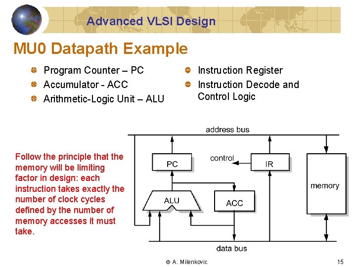
Advanced VLSI Design MU 0 Datapath Example Program Counter – PC Accumulator - ACC Arithmetic-Logic Unit – ALU Instruction Register Instruction Decode and Control Logic Follow the principle that the memory will be limiting factor in design: each instruction takes exactly the number of clock cycles defined by the number of memory accesses it must take. A. Milenkovic 15

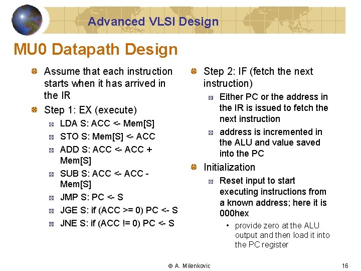
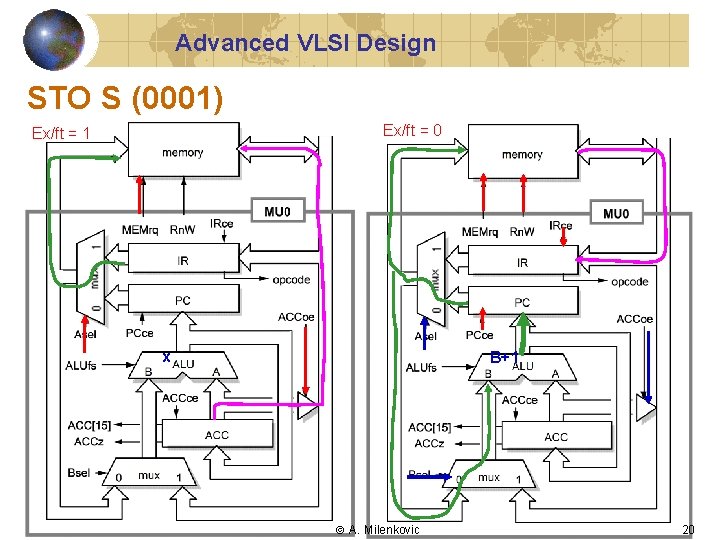
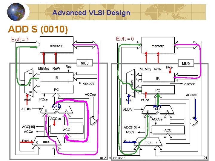
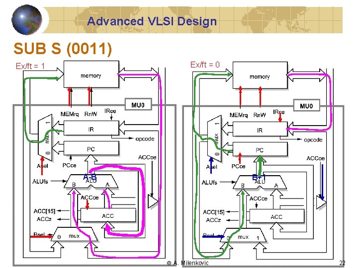
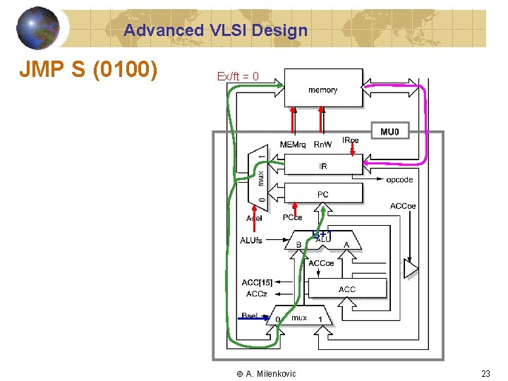
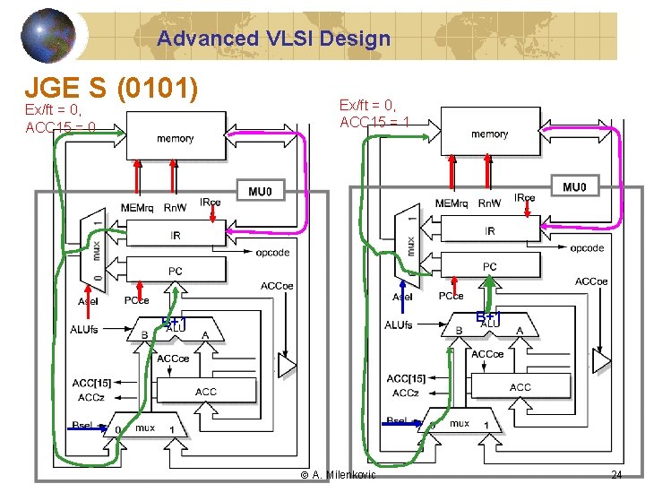
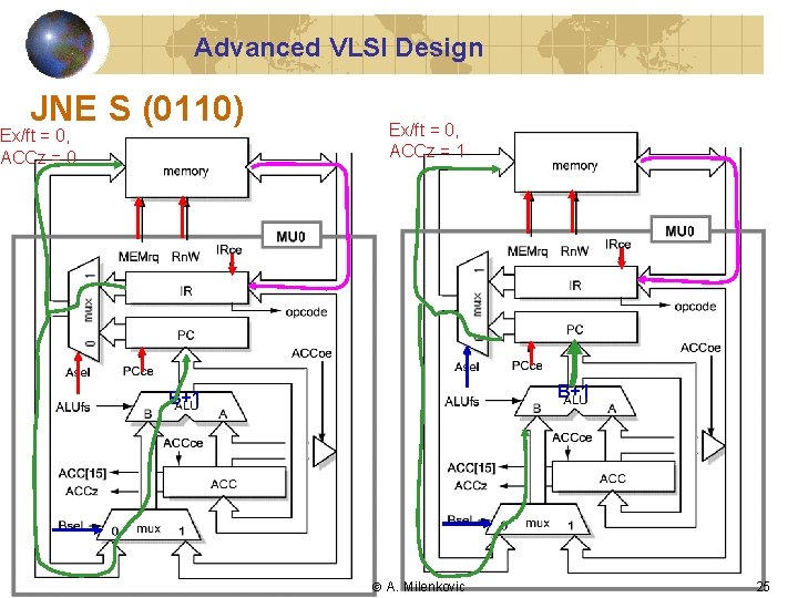
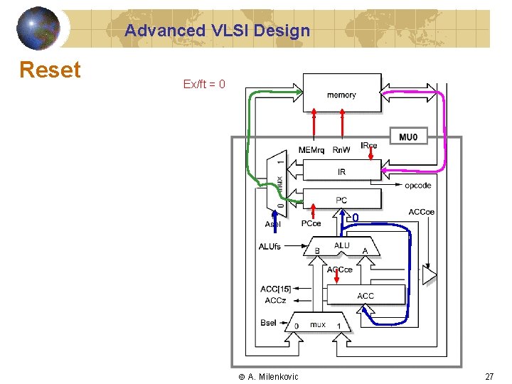
Advanced VLSI Design MU 0 Datapath Design Assume that each instruction starts when it has arrived in the IR Step 1: EX (execute) LDA S: ACC <- Mem[S] STO S: Mem[S] <- ACC ADD S: ACC <- ACC + Mem[S] SUB S: ACC <- ACC Mem[S] JMP S: PC <- S JGE S: if (ACC >= 0) PC <- S JNE S: if (ACC != 0) PC <- S Step 2: IF (fetch the next instruction) Either PC or the address in the IR is issued to fetch the next instruction address is incremented in the ALU and value saved into the PC Initialization A. Milenkovic Reset input to start executing instructions from a known address; here it is 000 hex • provide zero at the ALU output and then load it into the PC register 16

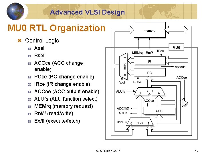
Advanced VLSI Design MU 0 RTL Organization Control Logic Asel Bsel ACCce (ACC change enable) PCce (PC change enable) IRce (IR change enable) ACCoe (ACC output enable) ALUfs (ALU function select) MEMrq (memory request) Rn. W (read/write) Ex/ft (execute/fetch) A. Milenkovic 17

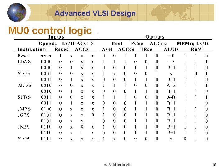
Advanced VLSI Design MU 0 control logic A. Milenkovic 18

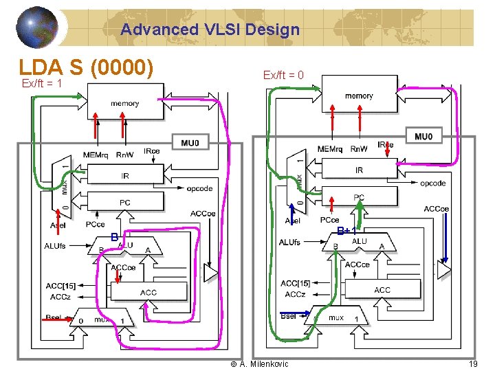
Advanced VLSI Design LDA S (0000) Ex/ft = 1 Ex/ft = 0 B+1 B A. Milenkovic 19

Advanced VLSI Design STO S (0001) Ex/ft = 0 Ex/ft = 1 x B+1 A. Milenkovic 20

Advanced VLSI Design ADD S (0010) Ex/ft = 0 Ex/ft = 1 A+B B+1 A. Milenkovic 21

Advanced VLSI Design SUB S (0011) Ex/ft = 0 Ex/ft = 1 A-B B+1 A. Milenkovic 22

Advanced VLSI Design JMP S (0100) Ex/ft = 0 B+1 A. Milenkovic 23

Advanced VLSI Design JGE S (0101) Ex/ft = 0, ACC 15 = 0 Ex/ft = 0, ACC 15 = 1 B+1 A. Milenkovic 24

Advanced VLSI Design JNE S (0110) Ex/ft = 0, ACCz = 0 Ex/ft = 0, ACCz = 1 B+1 A. Milenkovic 25

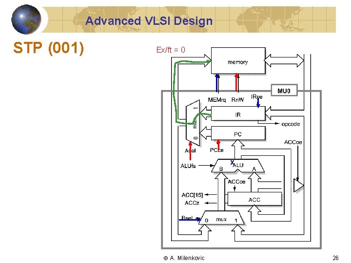
Advanced VLSI Design STP (001) Ex/ft = 0 x A. Milenkovic 26

Advanced VLSI Design Reset Ex/ft = 0 0 A. Milenkovic 27