Chapter 7 Designing Sequential Logic Circuits Rev 1
![TSPC-based Positive Edge. Triggered DFF From Referenced Textbooks: [1] “CMOS Integrated Circuits: Analysis and TSPC-based Positive Edge. Triggered DFF From Referenced Textbooks: [1] “CMOS Integrated Circuits: Analysis and](https://slidetodoc.com/presentation_image/0aa3eeb6dcefd5f8c8d086e24777c4d3/image-32.jpg)
- Slides: 44

Chapter 7 Designing Sequential Logic Circuits Rev 1. 0: 05/11/03 1. 1: 5/23/03 1. 2: 5/30/03

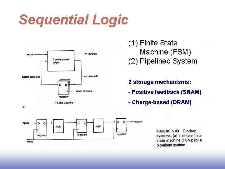
Sequential Logic (1) Finite State Machine (FSM) (2) Pipelined System 2 storage mechanisms: - Positive feedback (SRAM) - Charge-based (DRAM)

Naming Conventions q In our textbook: § a latch is Level-sensitive flip-flop § a register is Edge-triggered flip-flop q There are many different naming conventions § For instance, many books call Edgetriggered elements flip-flops (asynchronous JK, SR) This leads to confusion

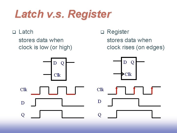
Latch v. s. Register q Latch stores data when clock is low (or high) q Register stores data when clock rises (on edges) D Q Clk Clk D D Q Q

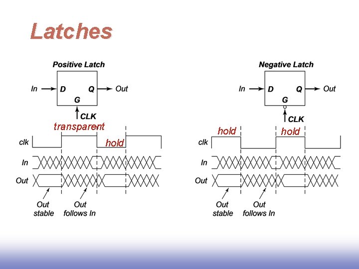
Latches transparent hold

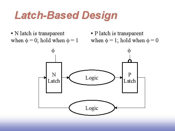
Latch-Based Design • N latch is transparent when f = 0; hold when f = 1 • P latch is transparent when f = 1; hold when f = 0 f f N Latch P Latch Logic

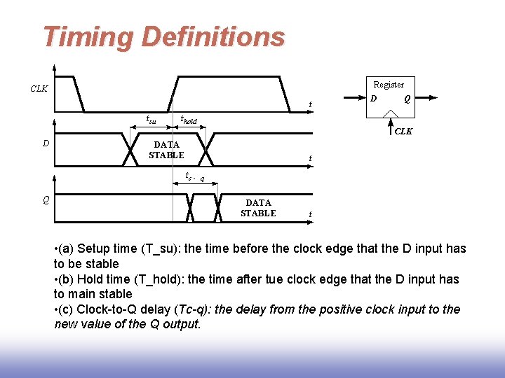
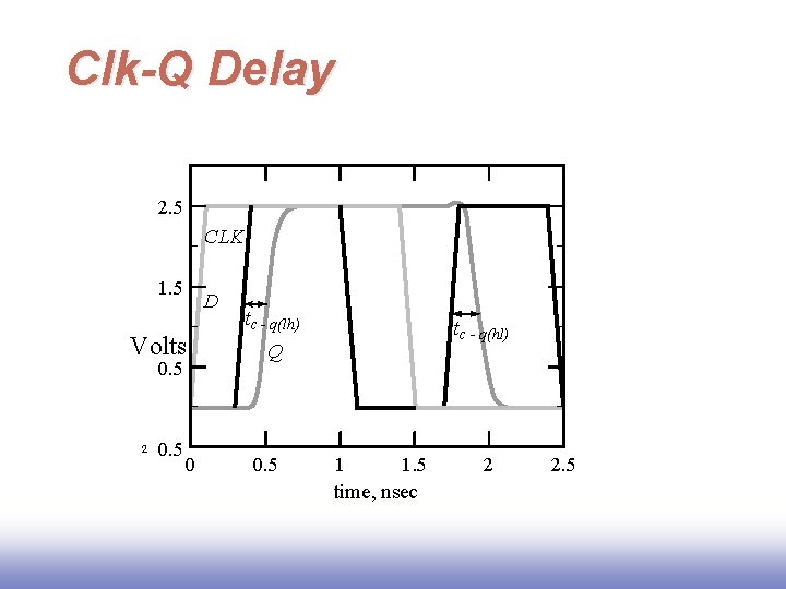
Timing Definitions Register CLK t tsu D Q thold CLK D DATA STABLE t tc - Q q DATA STABLE t • (a) Setup time (T_su): the time before the clock edge that the D input has to be stable • (b) Hold time (T_hold): the time after tue clock edge that the D input has to main stable • (c) Clock-to-Q delay (Tc-q): the delay from the positive clock input to the new value of the Q output.

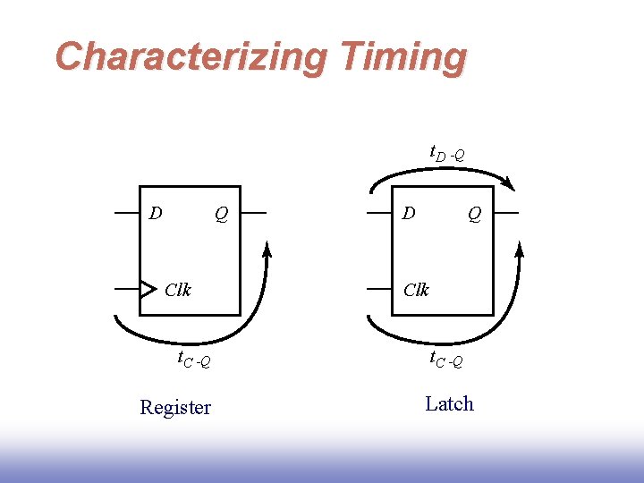
Characterizing Timing t. D -Q D Q Clk t. C -Q Register D Q Clk t. C -Q Latch

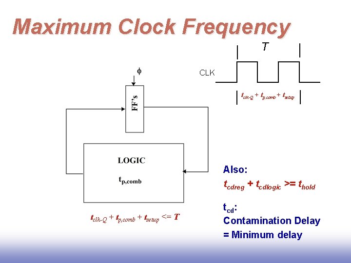
Maximum Clock Frequency T CLK tclk-Q + tp, comb + tsetup Also: tcdreg + tcdlogic >= thold tclk-Q + tp, comb + tsetup <= T tcd: Contamination Delay = Minimum delay

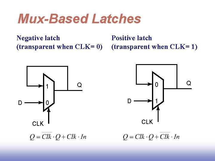
Mux-Based Latches Negative latch (transparent when CLK= 0) 1 D 0 CLK Positive latch (transparent when CLK= 1) 0 Q D 1 CLK Q

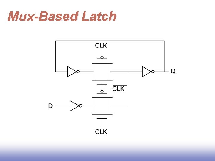
Mux-Based Latch

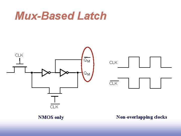
Mux-Based Latch CLK QM CLK NMOS only Non-overlapping clocks

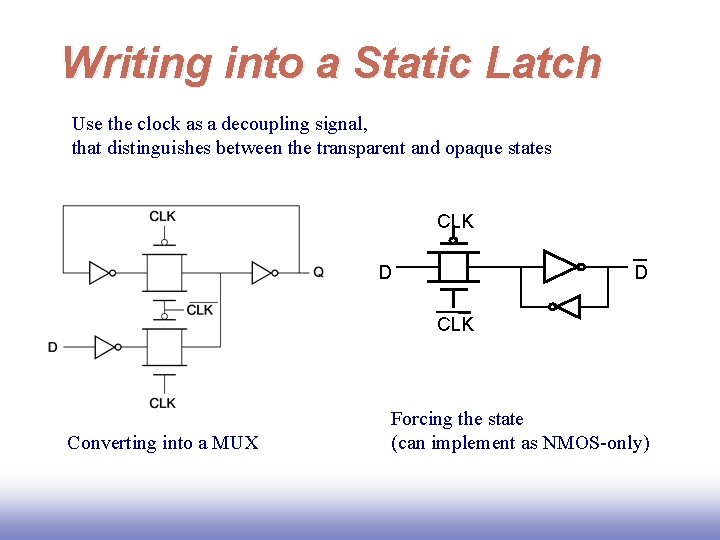
Writing into a Static Latch Use the clock as a decoupling signal, that distinguishes between the transparent and opaque states CLK D D CLK Converting into a MUX Forcing the state (can implement as NMOS-only)

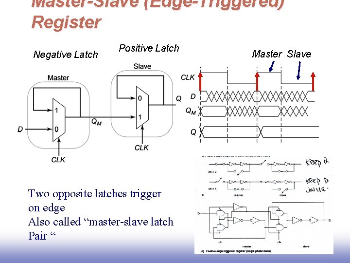
Master-Slave (Edge-Triggered) Register Negative Latch Positive Latch Two opposite latches trigger on edge Also called “master-slave latch Pair “ Master Slave

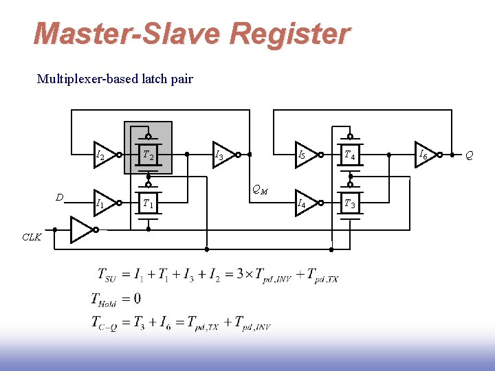
Master-Slave Register Multiplexer-based latch pair I 2 D CLK T 2 I 3 I 55 T 4 I 4 T 3 QM I 1 T 1 I 6 Q

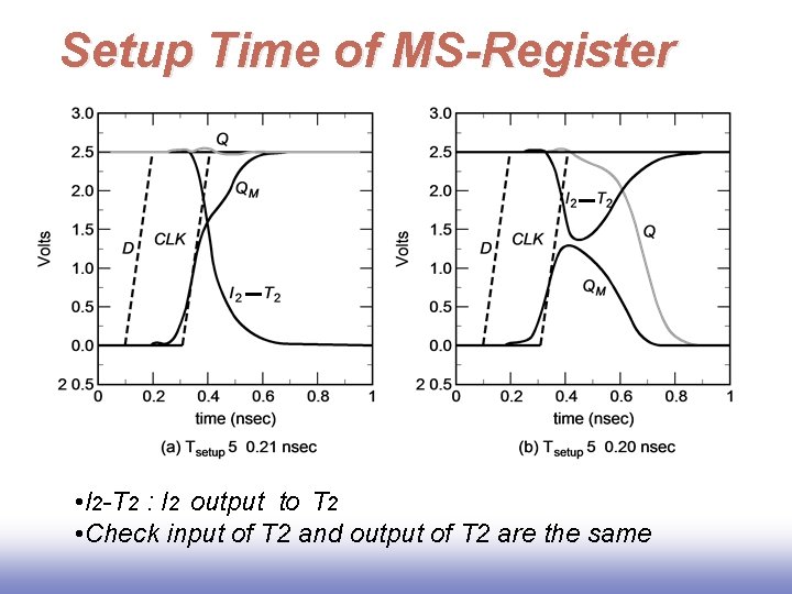
Setup Time of MS-Register • I 2 -T 2 : I 2 output to T 2 • Check input of T 2 and output of T 2 are the same

Clk-Q Delay 2. 5 CLK 1. 5 D Volts 0. 5 2 0. 5 0 tc - q(lh) tc - q(hl) Q 0. 5 1 1. 5 time, nsec 2 2. 5

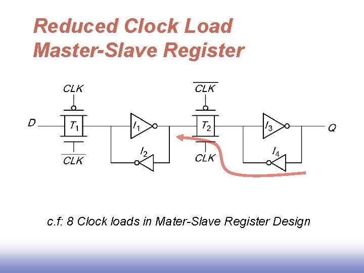
Reduced Clock Load Master-Slave Register c. f: 8 Clock loads in Mater-Slave Register Design

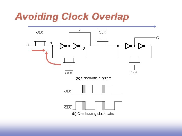
Avoiding Clock Overlap X CLK Q D A B CLK (a) Schematic diagram CLK (b) Overlapping clock pairs

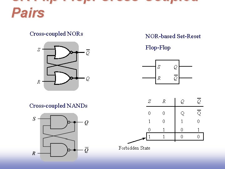
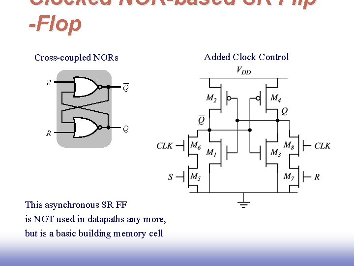
SR Flip-Flop: Cross-Coupled Pairs Cross-coupled NORs S R NOR-based Set-Reset Q Flop-Flop Q Cross-coupled NANDs S Q R Q S R Q Q 0 0 Q Q 1 0 0 1 1 1 0 0 1 0 Forbidden State

Clocked NOR-based SR Flip -Flop Added Clock Control Cross-coupled NORs S R Q Q This asynchronous SR FF is NOT used in datapaths any more, but is a basic building memory cell

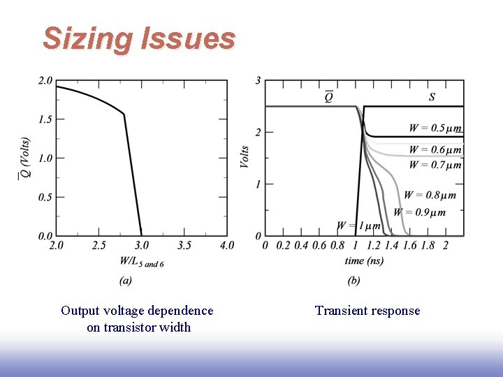
Sizing Issues Output voltage dependence on transistor width Transient response

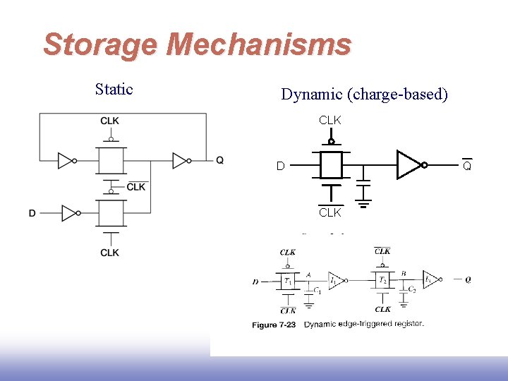
Storage Mechanisms Static Dynamic (charge-based) CLK D Q CLK

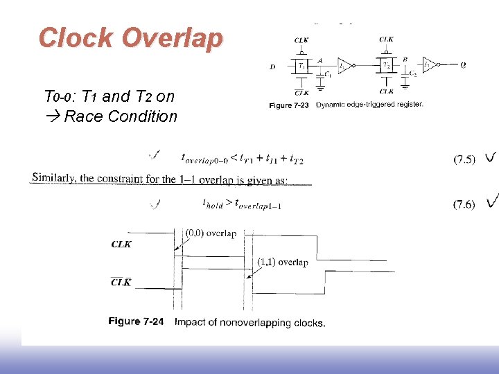
Clock Overlap T 0 -0: T 1 and T 2 on Race Condition

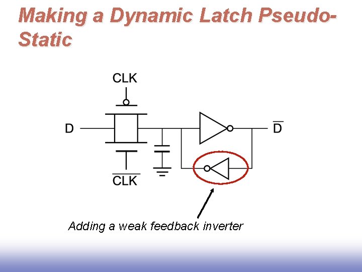
Making a Dynamic Latch Pseudo. Static Adding a weak feedback inverter

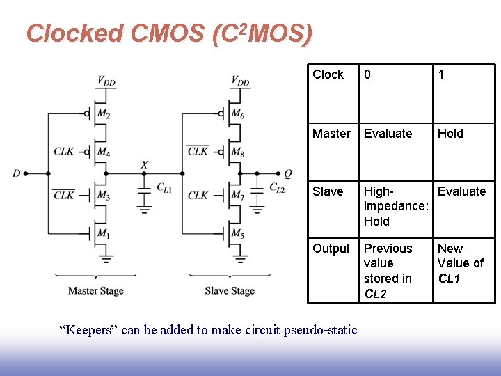
Clocked CMOS (C 2 MOS) Clock 0 1 Master Evaluate Hold Slave High. Evaluate impedance: Hold Output Previous value stored in CL 2 “Keepers” can be added to make circuit pseudo-static New Value of CL 1

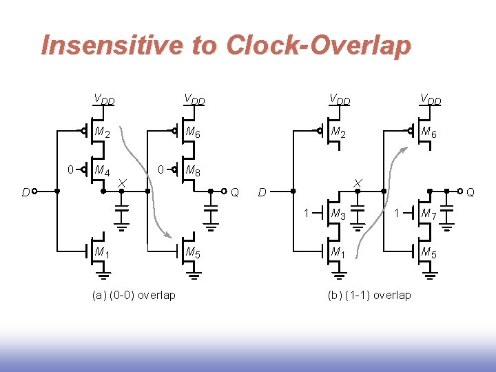
Insensitive to Clock-Overlap 0 VDD VDD M 2 M 6 M 4 D 0 X M 8 Q X D 1 M 1 (a) (0 -0) overlap M 5 M 3 Q 1 M 1 (b) (1 -1) overlap M 7 M 5

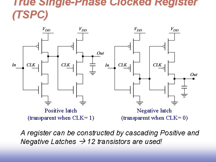
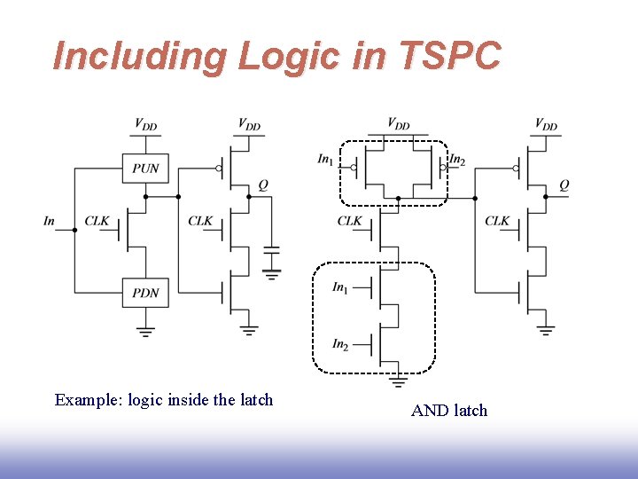
True Single-Phase Clocked Register (TSPC) Positive latch (transparent when CLK= 1) Negative latch (transparent when CLK= 0) A register can be constructed by cascading Positive and Negative Latches 12 transistors are used!

Including Logic in TSPC Example: logic inside the latch AND latch

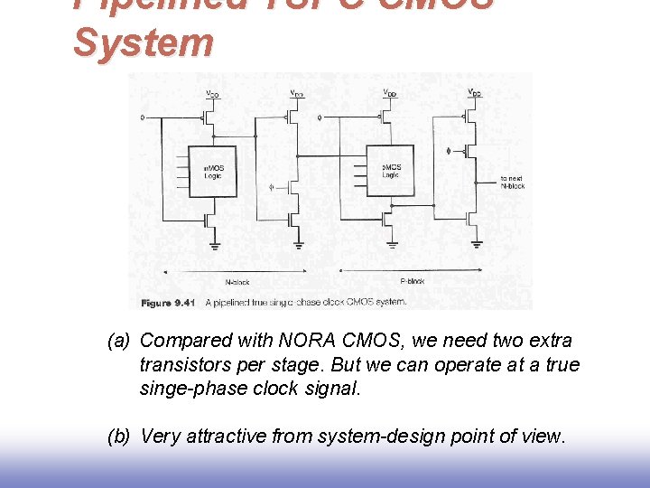
Pipelined TSPC CMOS System (a) Compared with NORA CMOS, we need two extra transistors per stage. But we can operate at a true singe-phase clock signal. (b) Very attractive from system-design point of view.

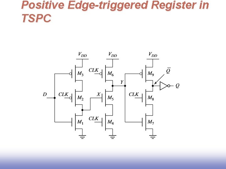
Positive Edge-triggered Register in TSPC
![TSPCbased Positive Edge Triggered DFF From Referenced Textbooks 1 CMOS Integrated Circuits Analysis and TSPC-based Positive Edge. Triggered DFF From Referenced Textbooks: [1] “CMOS Integrated Circuits: Analysis and](https://slidetodoc.com/presentation_image/0aa3eeb6dcefd5f8c8d086e24777c4d3/image-32.jpg)
TSPC-based Positive Edge. Triggered DFF From Referenced Textbooks: [1] “CMOS Integrated Circuits: Analysis and Design, ” 3 rd Ed. , by Sung-Mo Kang and Yusuf Leblebici, Mc. Graw-Hill, 2003.

Pipelined Systems using Dynamic CMOS Circuits

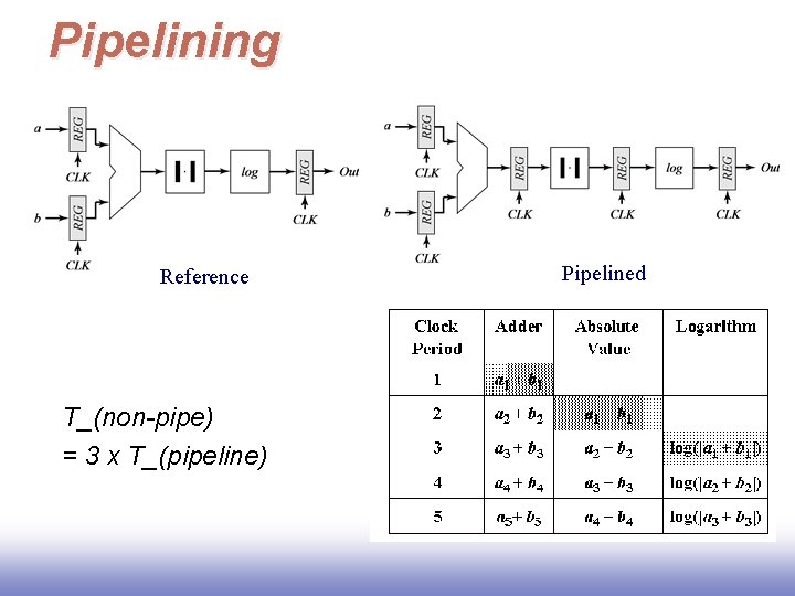
Pipelining Reference T_(non-pipe) = 3 x T_(pipeline) Pipelined

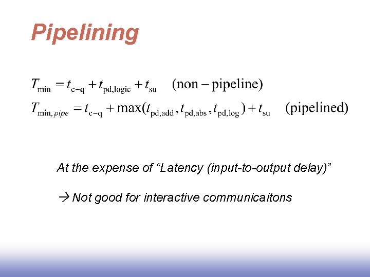
Pipelining At the expense of “Latency (input-to-output delay)” Not good for interactive communicaitons

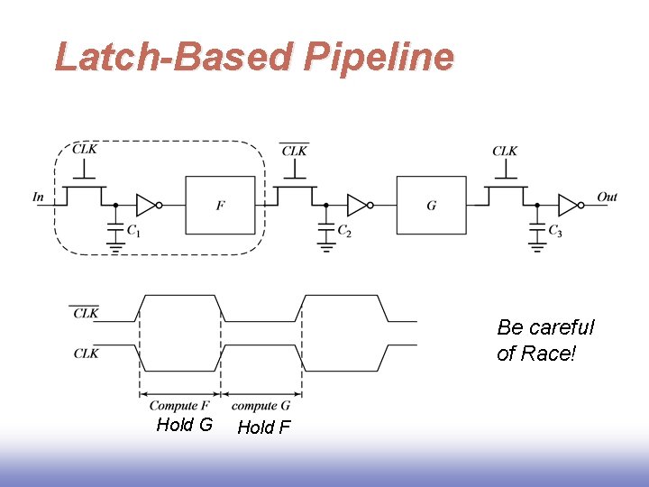
Latch-Based Pipeline Be careful of Race! Hold G Hold F

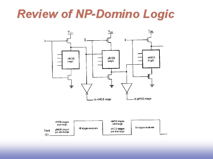
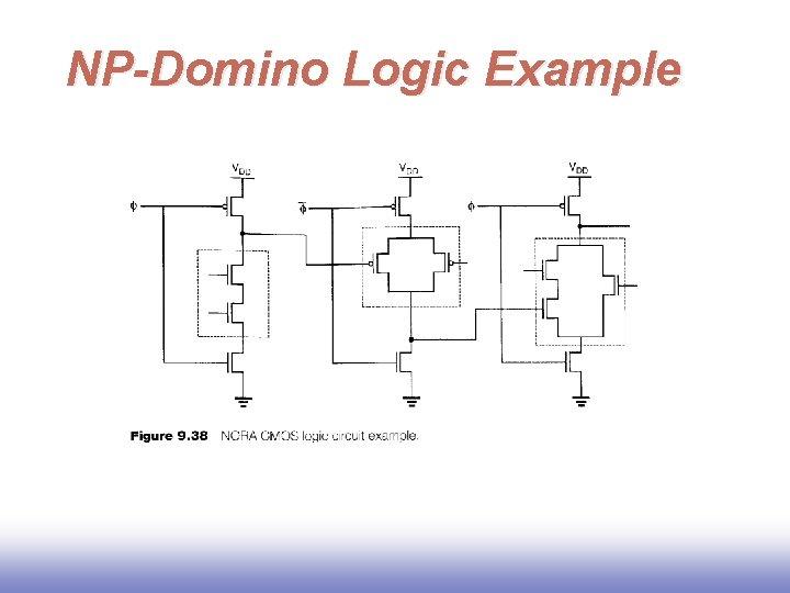
Review of NP-Domino Logic

NP-Domino Logic Example

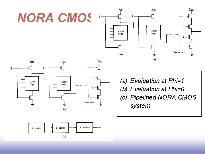
NORA CMOS (a) Evaluation at Phi=1 (b) Evaluation at Phi=0 (c) Pipelined NORA CMOS system

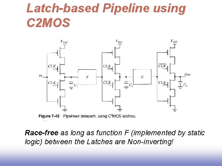
Latch-based Pipeline using C 2 MOS Race-free as long as function F (implemented by static logic) between the Latches are Non-inverting!

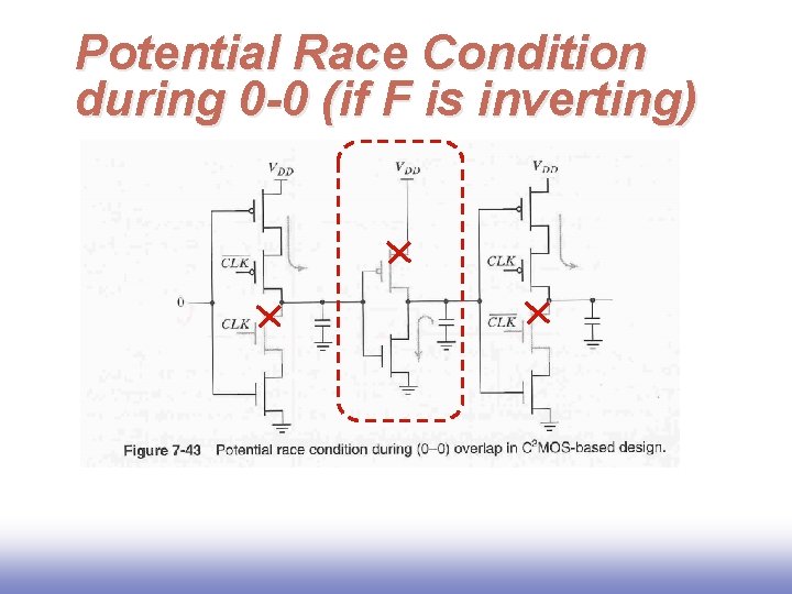
Potential Race Condition during 0 -0 (if F is inverting)

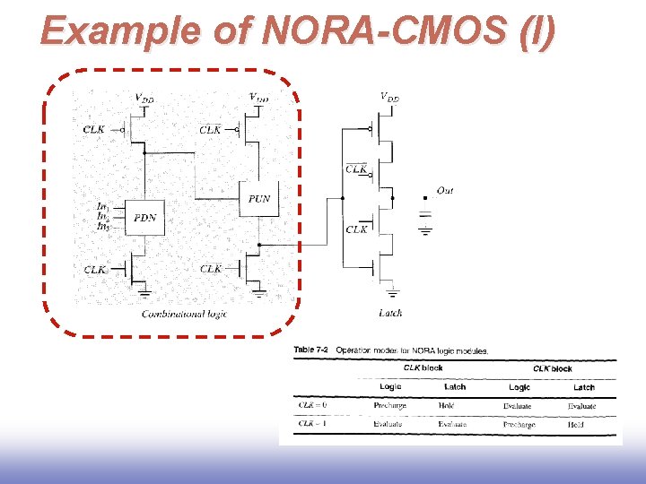
Example of NORA-CMOS (I)

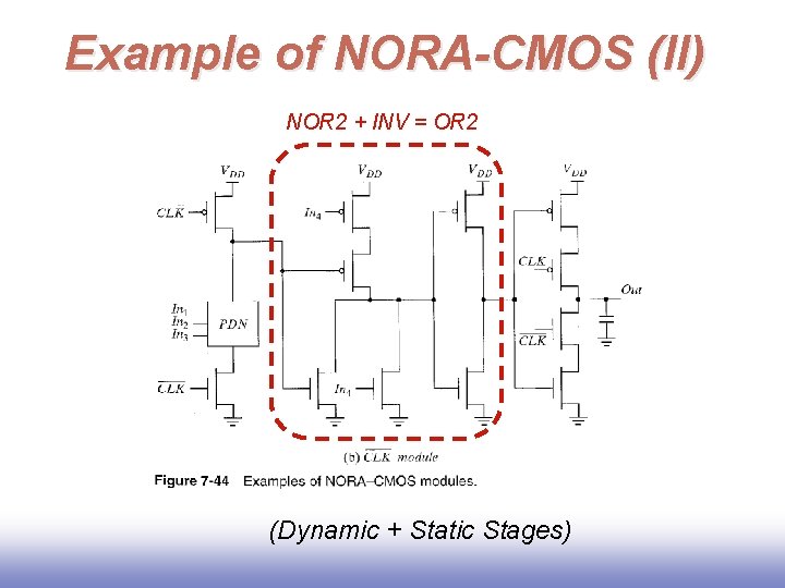
Example of NORA-CMOS (II) NOR 2 + INV = OR 2 (Dynamic + Static Stages)

Summary q Sequential circuits need good latches and registers for speed performance. q Dynamic circuits can realize the pipelined system in a very efficient and compact way. But it should be designed with extreme care. q Current trend is NOT to use dynamic CMOS for normal-speed operations good for design, maintain, and verification.