VLSI Physical Design Automation Clock and Power Routing

- Slides: 30

VLSI Physical Design Automation Clock and Power Routing Prof. David Pan dpan@ece. utexas. edu Office: ACES 5. 434 1

Routing of Clock and Power Nets • Different from other signal nets, clock and power are special routing problems – For clock nets, need to consider clock skew as well as delay. – For power nets, need to consider current density (IR drop) • => specialized routers for these nets. • Automatic tools for ASICs • Often manually routed and optimized for microprocessors, with help from automatic tools 2

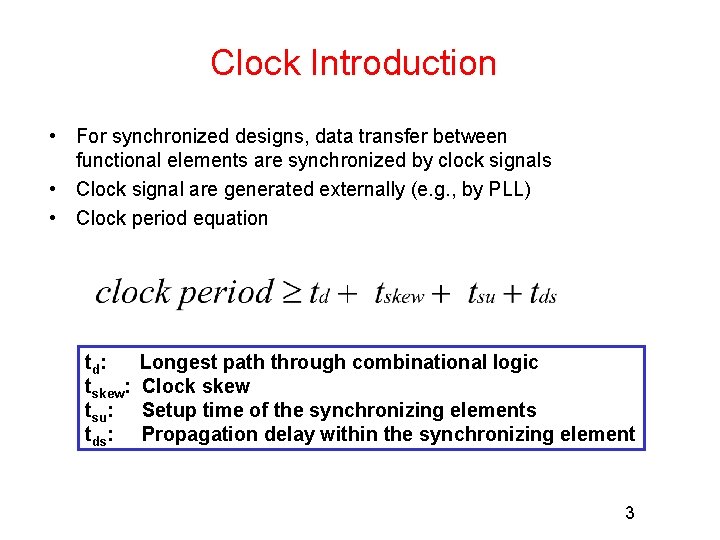
Clock Introduction • For synchronized designs, data transfer between functional elements are synchronized by clock signals • Clock signal are generated externally (e. g. , by PLL) • Clock period equation td : tskew: tsu: tds: Longest path through combinational logic Clock skew Setup time of the synchronizing elements Propagation delay within the synchronizing element 3

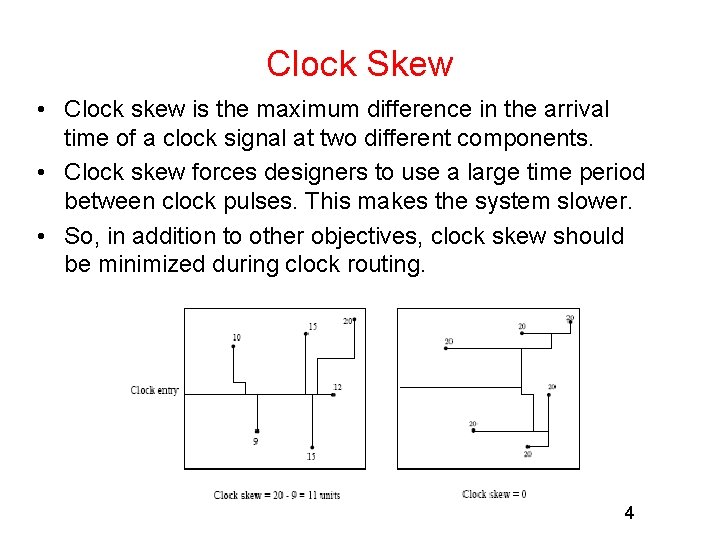
Clock Skew • Clock skew is the maximum difference in the arrival time of a clock signal at two different components. • Clock skew forces designers to use a large time period between clock pulses. This makes the system slower. • So, in addition to other objectives, clock skew should be minimized during clock routing. 4

Clock Design Problem • What are the main concerns for clock design? • Skew – No. 1 concern for clock networks – For increased clock frequency, skew may contribute over 10% of the system cycle time • Power – very important, as clock is a major power consumer! – It switches at every clock cycle! • Noise – Clock is often a very strong aggressor – May need shielding • Delay – Not really important – But slew rate is important (sharp transition) 5

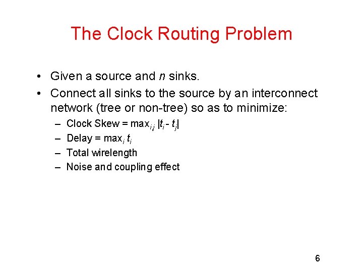
The Clock Routing Problem • Given a source and n sinks. • Connect all sinks to the source by an interconnect network (tree or non-tree) so as to minimize: – – Clock Skew = maxi, j |ti - tj| Delay = maxi ti Total wirelength Noise and coupling effect 6

Clock Design Considerations • Clock signal is global in nature, so clock nets are usually very big – Significant interconnect capacitance and resistance • So what are the techniques? – Routing • Clock tree versus clock mesh (non-tree or grid) • Balance skew and total wire length – Buffer insertion // will be covered in EE 382 V (Optimization issues in VLSI CAD) • Clock buffers to reduce clock skew, delay, and distortion in waveform. – Wire sizing // will be covered in Opt. Issues in VLSI CAD • To further tune the clock tree/mesh 7

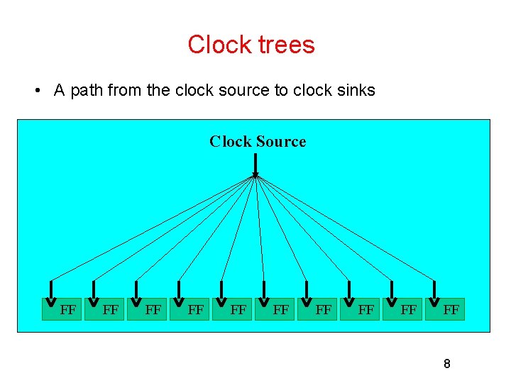
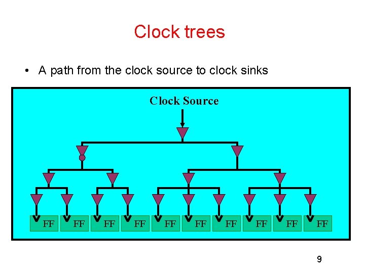
Clock trees • A path from the clock source to clock sinks Clock Source FF FF FF 8

Clock trees • A path from the clock source to clock sinks Clock Source FF FF FF 9

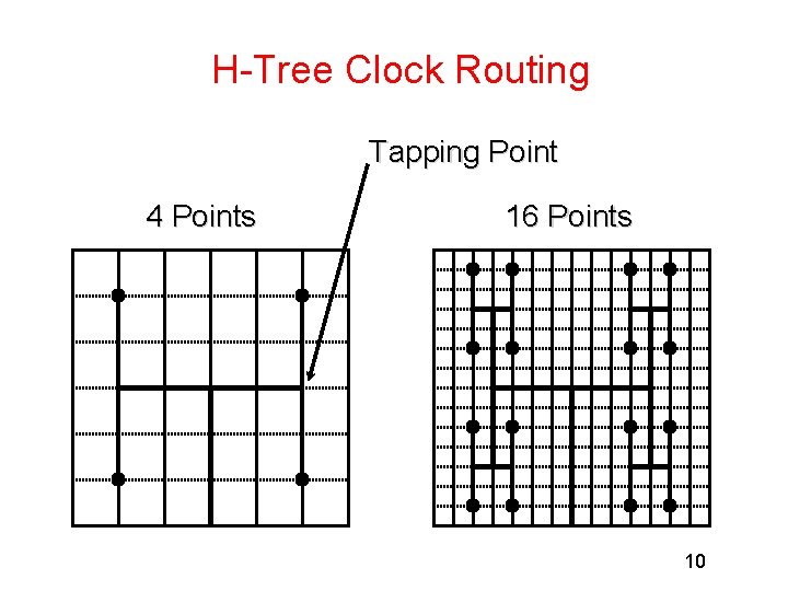
H-Tree Clock Routing Tapping Point 4 Points 16 Points 10

H-tree Algorithm • Minimize skew by making interconnections to subunits equal in length – Regular pattern – The skew is 0 assuming delay is directly proportional to wirelength • Is this always the case? ? ? • Can be used when terminals are evenly distributed – However, this is never the case in practice (due to blockage, and so on) – So strict (pure) H-trees are rarely used – However, still popular for top-level clock network design – Cons: too costly to be used everywhere Can you think of another shape if non-rectilinear wires are allowed? 11

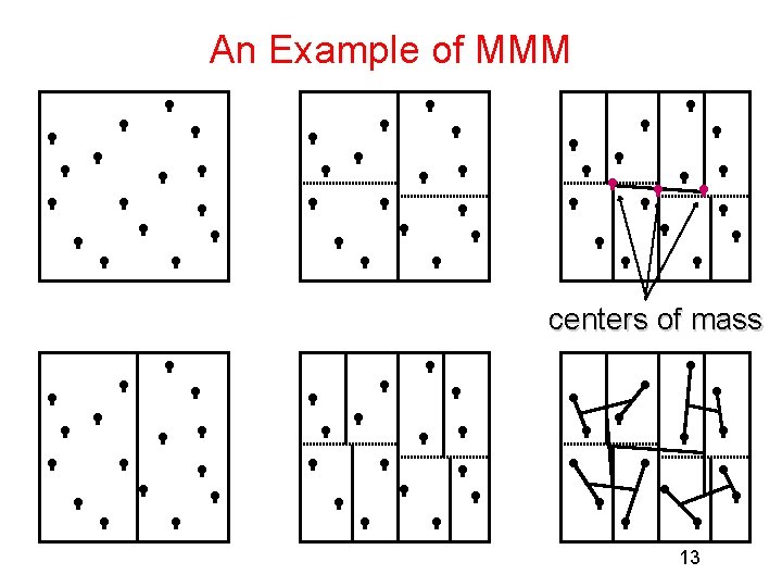
Method of Means and Medians (MMM) • Applicable when the clock terminals are arbitrarily arranged. • Follows a strategy very similar to H-Tree. • Recursively partition the terminals into two sets of equal size (median). Then, connect the center of mass of the whole circuit to the centers of mass of the two sub-circuits (mean). • Clock skew is only minimized heuristically. The resulting tree may not have zero-skew. 12

An Example of MMM centers of mass 13

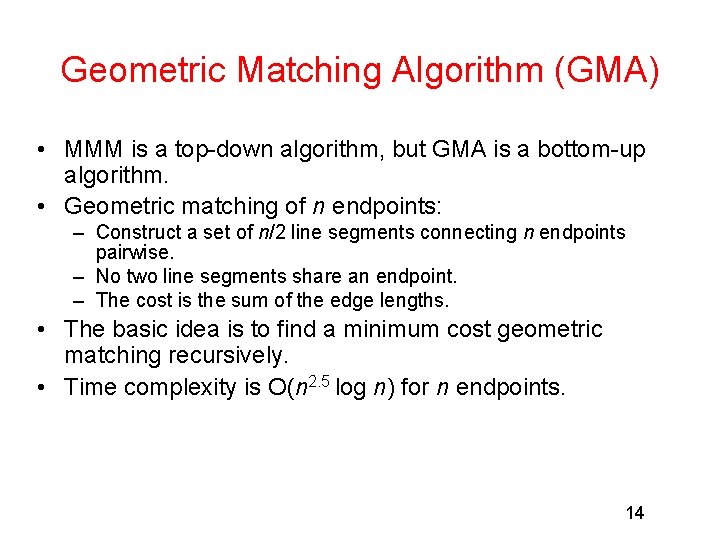
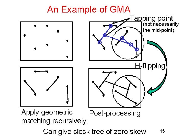
Geometric Matching Algorithm (GMA) • MMM is a top-down algorithm, but GMA is a bottom-up algorithm. • Geometric matching of n endpoints: – Construct a set of n/2 line segments connecting n endpoints pairwise. – No two line segments share an endpoint. – The cost is the sum of the edge lengths. • The basic idea is to find a minimum cost geometric matching recursively. • Time complexity is O(n 2. 5 log n) for n endpoints. 14

An Example of GMA Tapping point (not necessarily the mid-point) H-flipping Apply geometric Post-processing matching recursively. Can give clock tree of zero skew. 15

An Exact Zero Skew Algorithm • • ICCAD 1991 and TCAD 1993, Ren-Song Tsay A classic paper to manage clock skew Use Elmore delay model to compute delay Guarantee zero skew – Can easily to extended for zero skew or bounded skew – Can you think of a method to do it? • Try to minimize wire length, but not done very well – Lots of follow up works to minimize total wire length while maintaining zero skew – DME and its extensions 16

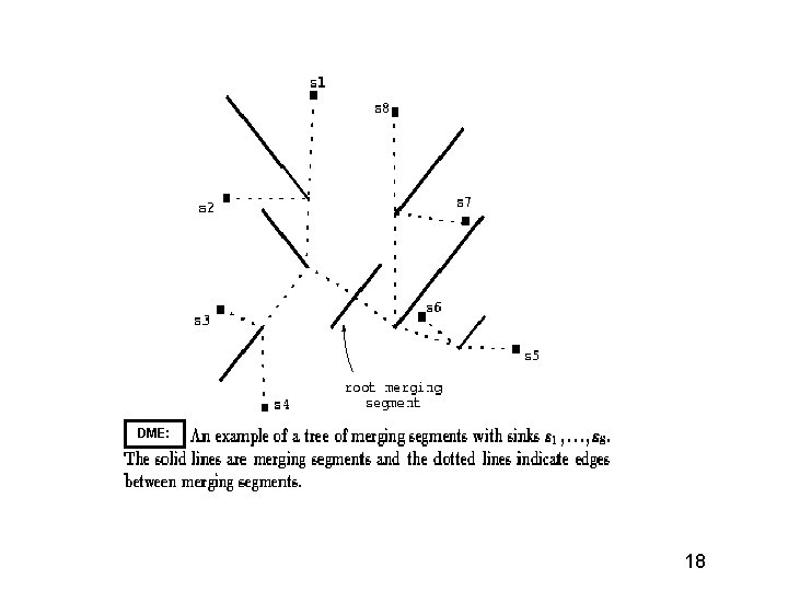
Deferred Merge Embedding • As its name implies, DME defers the merging as late as possible, to make sure minimal wire length cost for merging • Independently proposed by several groups – Edahiro, NEC Res Dev, 1991 – Chao et al, DAC’ 92 – Boese and Kahng, ASIC’ 92 • DME needs an abstract routing topology as the input • It has a bottom-up phase followed by a top-down process (sounds familiar? ) 17

DME: 18

Some Thoughts/Trend • Clock skew scheduling together with clock tree synthesis – Schedule the timing slack of a circuit to the individual registers for optimal performance and as a second criteria to increase the robustness of the implementation w. r. t. process variation. • Variability is a major nanometer concern • Non-tree clock networks for variation-tolerance – How to analyze it? – The task is to investigate a combined optimization such that clock skew variability is reduced with minimum wirelength penalty 19

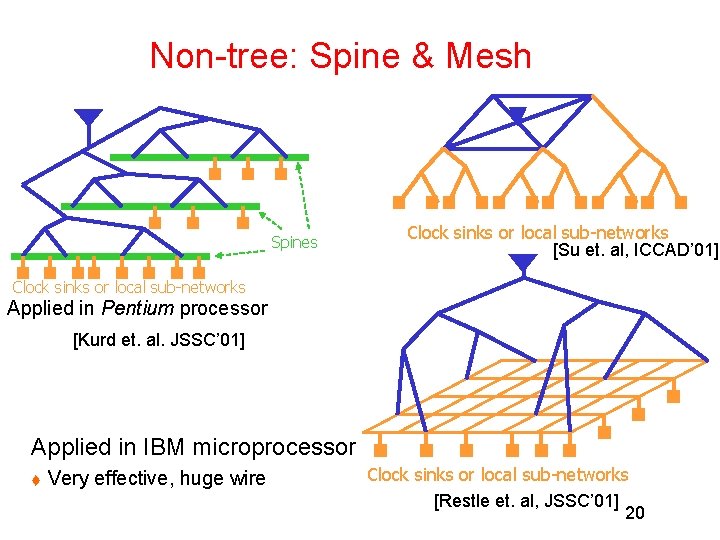
Non-tree: Spine & Mesh Spines Clock sinks or local sub-networks [Su et. al, ICCAD’ 01] Clock sinks or local sub-networks Applied in Pentium processor [Kurd et. al. JSSC’ 01] Applied in IBM microprocessor t Very effective, huge wire Clock sinks or local sub-networks [Restle et. al, JSSC’ 01] 20

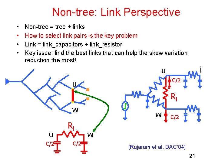
Non-tree: Link Perspective • • Non-tree = tree + links How to select link pairs is the key problem Link = link_capacitors + link_resistor Key issue: find the best links that can help the skew variation reduction the most! i u C/2 u Rl w u C/2 Rl C/2 w [Rajaram et al, DAC’ 04] 21

Power Distribution/Routing 22

Power Distribution • Power Distribution Network functions – – – – Carry current from pads to transistors on chip Maintain stable voltage with low noise Provide average and peak power demands Provide current return paths for signals Avoid electromigration & self-heating wearout Consume little chip area and wire Easy to lay out 23

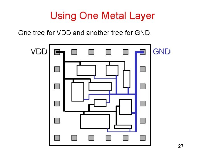
Power and Ground Routing • Each standard cell or macro has power and ground signals, i. e. , Vdd (power) and GND (ground) • They need to be connected as well • You can imagine that they are HUGE NETWORKS! • In general, P/G routings are pretty regular • They have high priority as well – P/G routing resources are usually reserved – When you do global and detailed routing for signal nets, you cannot use up all the routing resources at each metal layers • Normally some design rules will be given (e. g. , 40% of top metal layers are reserved for P/G) 24

P/G Routing Main Objectives • Routing resource – Need to balance the routing resource for P/G, clock and signals • Voltage drop – – Static (IR) and dynamic (L di/dt) voltage drops More voltage drop means more gate delay Usually less than 5 -10% voltage drop is allowed So you may need to size P/G wires accordingly • Electrical migration – Too big current may cause EMI problem • Others… 25

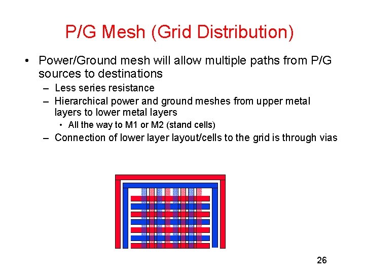
P/G Mesh (Grid Distribution) • Power/Ground mesh will allow multiple paths from P/G sources to destinations – Less series resistance – Hierarchical power and ground meshes from upper metal layers to lower metal layers • All the way to M 1 or M 2 (stand cells) – Connection of lower layout/cells to the grid is through vias 26

Using One Metal Layer One tree for VDD and another tree for GND. VDD GND 27

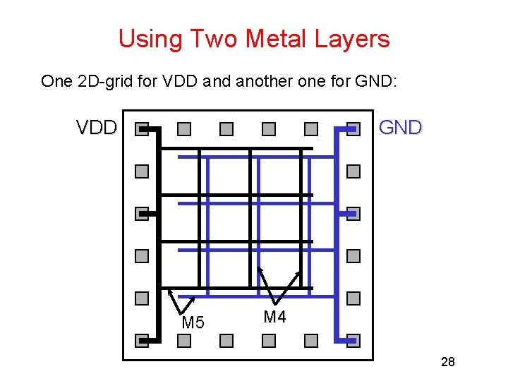
Using Two Metal Layers One 2 D-grid for VDD and another one for GND: VDD GND M 5 M 4 28

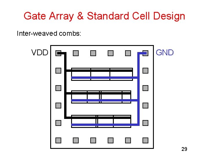
Gate Array & Standard Cell Design Inter-weaved combs: VDD GND 29

Some Thoughts/Trends • P/G I/O pad co-optimization with classic physical design • Decoupling capacitor can reduce P/G related voltage drop – Need to be planned together with floorplanning and placement • Multiple voltage/frequency islands make the P/G problem and clock distributions more challenging 30