Effective IDDQ Testing method to identify the fault
![Problem statement For new Technologies (Deep submicron levels) Earlier Technologies[1] Low threshold Transistors Higher Problem statement For new Technologies (Deep submicron levels) Earlier Technologies[1] Low threshold Transistors Higher](https://slidetodoc.com/presentation_image_h/0140032f80fc7090f5cd876d3e9f6608/image-4.jpg)
![Proposed Method § IDDQ versus Temperature[2] st Robu Low er Pow VLSI ΔIDDQ(Faulty)<<IDDQ(Defect free) Proposed Method § IDDQ versus Temperature[2] st Robu Low er Pow VLSI ΔIDDQ(Faulty)<<IDDQ(Defect free)](https://slidetodoc.com/presentation_image_h/0140032f80fc7090f5cd876d3e9f6608/image-5.jpg)
![References § § § st Robu Low er Pow VLSI [1]. S. Sabade and References § § § st Robu Low er Pow VLSI [1]. S. Sabade and](https://slidetodoc.com/presentation_image_h/0140032f80fc7090f5cd876d3e9f6608/image-20.jpg)
- Slides: 20

Effective IDDQ Testing method to identify the fault in Low-Voltage CMOS Circuits st Robu Low ECE er Pow 7502 LSI V S 2015 ECE 7502 Project Final Presentation W. P Manula Pathirana 21 st April 2015

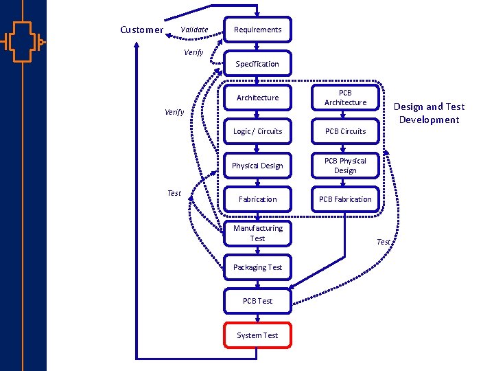
Customer Validate Requirements Verify Specification Architecture PCB Architecture Logic / Circuits PCB Circuits Physical Design PCB Physical Design Fabrication PCB Fabrication Verify Test Manufacturing Test Packaging Test st Robu Low er Pow VLSI PCB Test System Test Design and Test Development Test

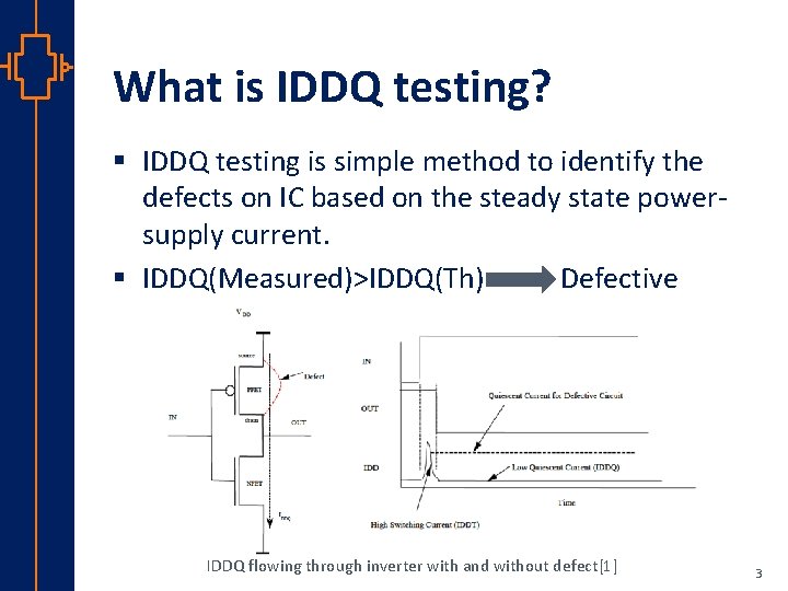
What is IDDQ testing? § IDDQ testing is simple method to identify the defects on IC based on the steady state powersupply current. § IDDQ(Measured)>IDDQ(Th) Defective st Robu Low er Pow VLSI IDDQ flowing through inverter with and without defect[1] 3
![Problem statement For new Technologies Deep submicron levels Earlier Technologies1 Low threshold Transistors Higher Problem statement For new Technologies (Deep submicron levels) Earlier Technologies[1] Low threshold Transistors Higher](https://slidetodoc.com/presentation_image_h/0140032f80fc7090f5cd876d3e9f6608/image-4.jpg)
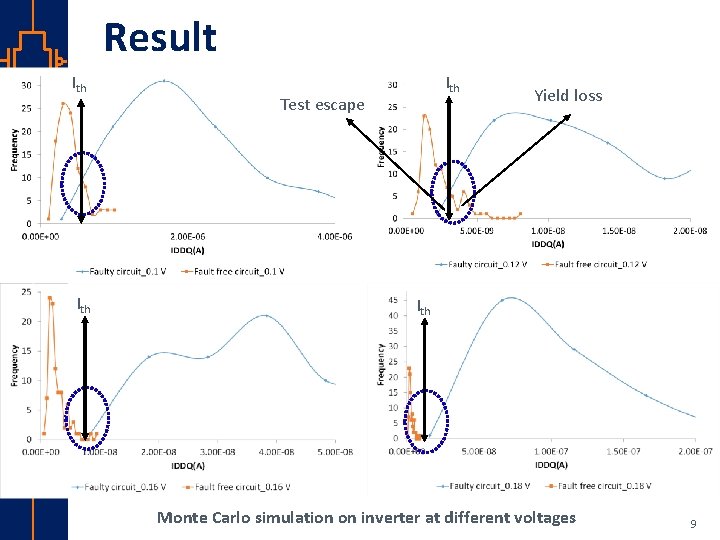
Problem statement For new Technologies (Deep submicron levels) Earlier Technologies[1] Low threshold Transistors Higher Leakage IDDQ(Fault Free)≈IDDQ(Defective) Deep submicron Technologies[1] Test escapes and yield loss st Robu Low er Pow VLSI [1]S. Sabade and D. M. Walker, “I DDX-based test methods: A survey, ” ACM Trans. Des. Autom. Electron. Syst. TODAES, vol. 9, no. 2, pp. 159– 198, 2004. A-test escapes B-yield loss 4
![Proposed Method IDDQ versus Temperature2 st Robu Low er Pow VLSI ΔIDDQFaultyIDDQDefect free Proposed Method § IDDQ versus Temperature[2] st Robu Low er Pow VLSI ΔIDDQ(Faulty)<<IDDQ(Defect free)](https://slidetodoc.com/presentation_image_h/0140032f80fc7090f5cd876d3e9f6608/image-5.jpg)
Proposed Method § IDDQ versus Temperature[2] st Robu Low er Pow VLSI ΔIDDQ(Faulty)<<IDDQ(Defect free) Low temperature measurement is undesirable in production due to high cost [2]A. Kaltchenko and O. Semenov, “Temperature dependence of IDDQ distribution: application for thermal delta IDDQ testing, ” IET Circuits, Devices & Systems, vol. 1, no. 6, p. 509, 2007. 5

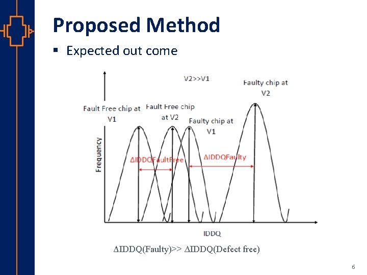
Proposed Method § Expected out come st Robu Low er Pow VLSI ΔIDDQ(Faulty)>> ∆IDDQ(Defect free) 6

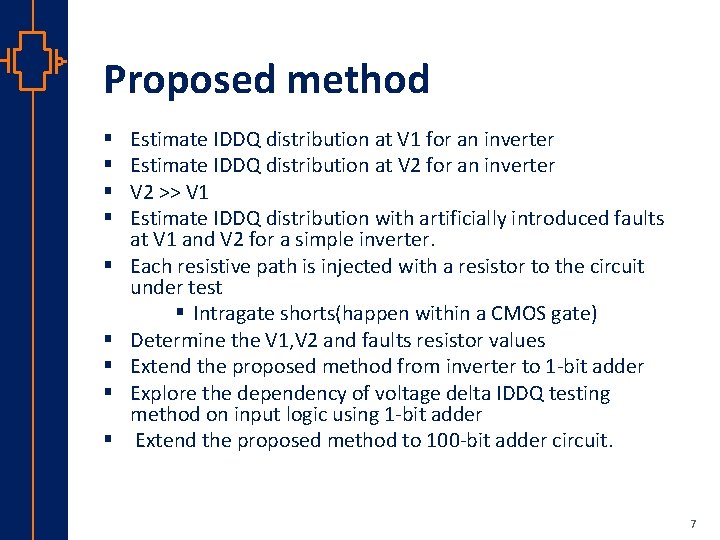
Proposed method § § § § st Robu Low er Pow VLSI § Estimate IDDQ distribution at V 1 for an inverter Estimate IDDQ distribution at V 2 for an inverter V 2 >> V 1 Estimate IDDQ distribution with artificially introduced faults at V 1 and V 2 for a simple inverter. Each resistive path is injected with a resistor to the circuit under test § Intragate shorts(happen within a CMOS gate) Determine the V 1, V 2 and faults resistor values Extend the proposed method from inverter to 1 -bit adder Explore the dependency of voltage delta IDDQ testing method on input logic using 1 -bit adder Extend the proposed method to 100 -bit adder circuit. 7

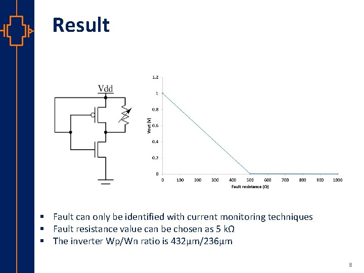
Result st Robu Low er Pow VLSI § Fault can only be identified with current monitoring techniques § Fault resistance value can be chosen as 5 kΩ § The inverter Wp/Wn ratio is 432µm/236µm 8

Result Ith Ith Test escape Yield loss Ith st Robu Low er Pow VLSI Monte Carlo simulation on inverter at different voltages 9

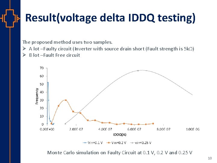
Result(voltage delta IDDQ testing) The proposed method uses two samples. Ø A lot –Faulty circuit (Inverter with source drain short (Fault strength is 5 kΩ) Ø B lot –Fault Free circuit st Robu Low er Pow VLSI Monte Carlo simulation on Faulty Circuit at 0. 1 V, 0. 2 V and 0. 25 V 10

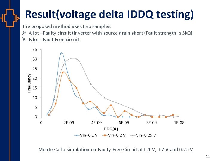
Result(voltage delta IDDQ testing) The proposed method uses two samples. Ø A lot –Faulty circuit (Inverter with source drain short (Fault strength is 5 kΩ) Ø B lot –Fault Free circuit st Robu Low er Pow VLSI Monte Carlo simulation on Faulty Free Circuit at 0. 1 V, 0. 2 V and 0. 25 V 11

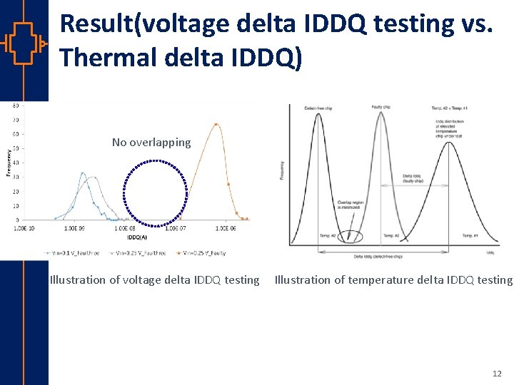
Result(voltage delta IDDQ testing vs. Thermal delta IDDQ) No overlapping Illustration of voltage delta IDDQ testing Illustration of temperature delta IDDQ testing st Robu Low er Pow VLSI 12

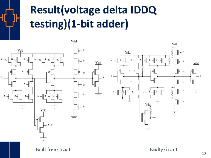
Result(voltage delta IDDQ testing)(1 -bit adder) st Robu Low er Pow VLSI Fault free circuit Faulty circuit 13

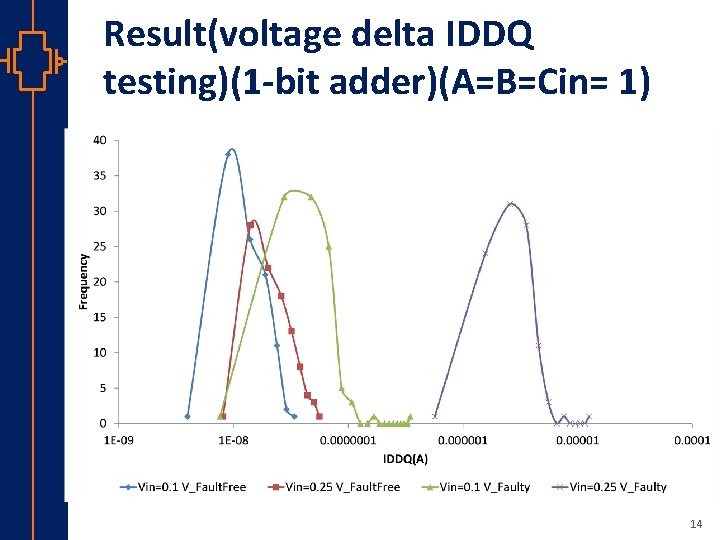
Result(voltage delta IDDQ testing)(1 -bit adder)(A=B=Cin= 1) st Robu Low er Pow VLSI 14

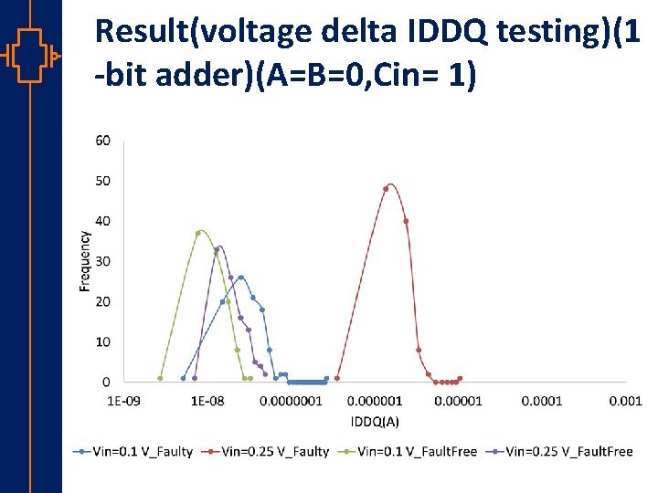
Result(voltage delta IDDQ testing)(1 -bit adder)(A=B=0, Cin= 1) st Robu Low er Pow VLSI 15

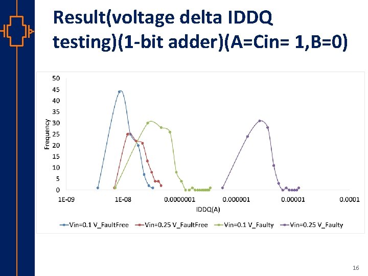
Result(voltage delta IDDQ testing)(1 -bit adder)(A=Cin= 1, B=0) st Robu Low er Pow VLSI 16

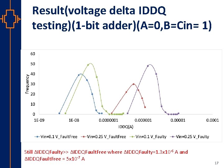
Result(voltage delta IDDQ testing)(1 -bit adder)(A=0, B=Cin= 1) st Robu Low er Pow VLSI Still ∆IDDQFaulty>> ∆IDDQFault. Free where ∆IDDQFaulty=1. 3 x 10 -6 A and ∆IDDQFault. Free = 5 x 10 -7 A 17

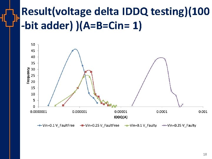
Result(voltage delta IDDQ testing)(100 -bit adder) )(A=B=Cin= 1) st Robu Low er Pow VLSI 18

Conclusion § Voltage delta IDDQ testing method is introduced. § The method is implemented on inverter, 1 -bit adder and 100 -bit adder circuit. § By looking at ∆IDDQ on different voltage defected chip can be identified. (Usually ∆IDDQFaulty>> ∆IDDQFault. Free) st Robu Low er Pow VLSI 19
![References st Robu Low er Pow VLSI 1 S Sabade and References § § § st Robu Low er Pow VLSI [1]. S. Sabade and](https://slidetodoc.com/presentation_image_h/0140032f80fc7090f5cd876d3e9f6608/image-20.jpg)
References § § § st Robu Low er Pow VLSI [1]. S. Sabade and D. M. Walker, “I DDX-based test methods: A survey, ” ACM Trans. Des. Autom. Electron. Syst. TODAES, vol. 9, no. 2, pp. 159– 198, 2004. [2]. A. Kaltchenko and O. Semenov, “Temperature dependence of IDDQ distribution: application for thermal delta IDDQ testing, ” IET Circuits, Devices & Systems, vol. 1, no. 6, p. 509, 2007. [3]. A. Abdollahi, F. Fallah, and M. Pedram, “Leakage current reduction in CMOS VLSI circuits by input vector control, ” IEEE Transactions on Very Large Scale Integration (VLSI) Systems, vol. 12, no. 2, pp. 140– 154, Feb. 2004. [4]. Z. Chen, L. Wei, and K. Roy, “On effective I/sub DDQ/testing of low-voltage CMOS circuits using leakage control techniques, ” Very Large Scale Integration (VLSI) Systems, IEEE Transactions on, vol. 9, no. 5, pp. 718– 725, 2001. [5]. M. Karmani, C. Khedhiri, and B. Hamdi, “Design and test challenges in Nano-scale analog and mixed CMOS technology, ” International Journal of VLSI design & Communication Systems (VLSICS) Vol, vol. 2, 2011. 20