Introduction to CMOS VLSI Design Circuit Pitfalls 1

- Slides: 38

Introduction to CMOS VLSI Design Circuit Pitfalls 1

Outline q Circuit Pitfalls – Detective puzzle – Given circuit and symptom, diagnose cause and recommend solution – All these pitfalls have caused failures in real chips q Noise Budgets q Reliability Circuit Pitfalls CMOS VLSI Design 2

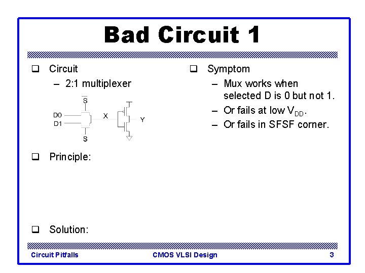
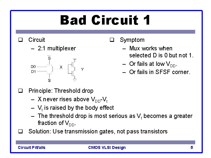
Bad Circuit 1 q Circuit – 2: 1 multiplexer q Symptom – Mux works when selected D is 0 but not 1. – Or fails at low VDD. – Or fails in SFSF corner. q Principle: q Solution: Circuit Pitfalls CMOS VLSI Design 3

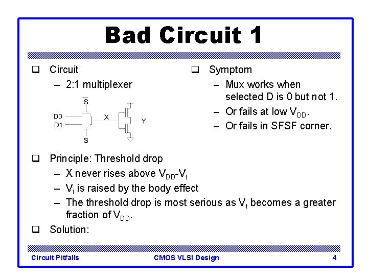
Bad Circuit 1 q Circuit – 2: 1 multiplexer q Symptom – Mux works when selected D is 0 but not 1. – Or fails at low VDD. – Or fails in SFSF corner. q Principle: Threshold drop – X never rises above VDD-Vt – Vt is raised by the body effect – The threshold drop is most serious as Vt becomes a greater fraction of VDD. q Solution: Circuit Pitfalls CMOS VLSI Design 4

Bad Circuit 1 q Circuit – 2: 1 multiplexer q Symptom – Mux works when selected D is 0 but not 1. – Or fails at low VDD. – Or fails in SFSF corner. q Principle: Threshold drop – X never rises above VDD-Vt – Vt is raised by the body effect – The threshold drop is most serious as Vt becomes a greater fraction of VDD. q Solution: Use transmission gates, not pass transistors Circuit Pitfalls CMOS VLSI Design 5

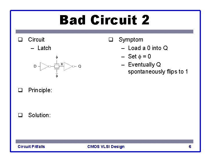
Bad Circuit 2 q Circuit – Latch q Symptom – Load a 0 into Q – Set f = 0 – Eventually Q spontaneously flips to 1 q Principle: q Solution: Circuit Pitfalls CMOS VLSI Design 6

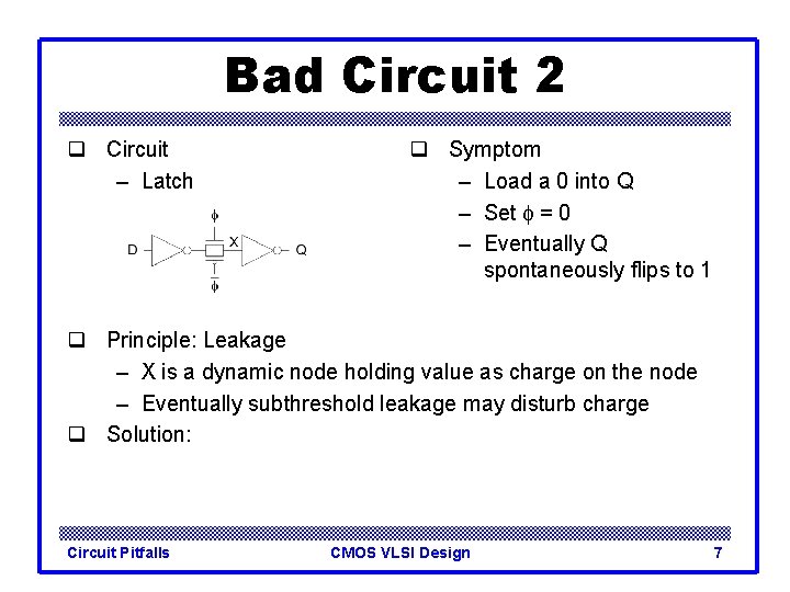
Bad Circuit 2 q Circuit – Latch q Symptom – Load a 0 into Q – Set f = 0 – Eventually Q spontaneously flips to 1 q Principle: Leakage – X is a dynamic node holding value as charge on the node – Eventually subthreshold leakage may disturb charge q Solution: Circuit Pitfalls CMOS VLSI Design 7

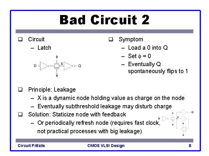
Bad Circuit 2 q Circuit – Latch q Symptom – Load a 0 into Q – Set f = 0 – Eventually Q spontaneously flips to 1 q Principle: Leakage – X is a dynamic node holding value as charge on the node – Eventually subthreshold leakage may disturb charge q Solution: Staticize node with feedback – Or periodically refresh node (requires fast clock, not practical processes with big leakage) Circuit Pitfalls CMOS VLSI Design 8

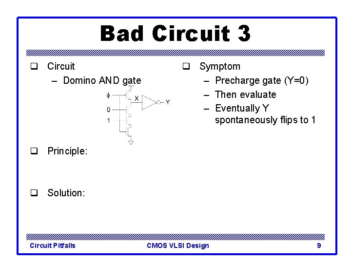
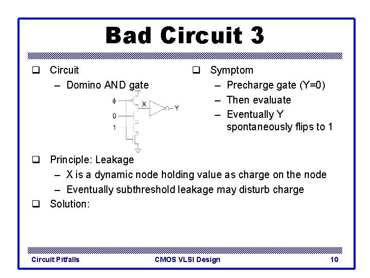
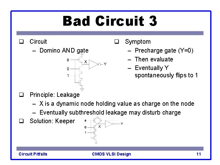
Bad Circuit 3 q Circuit – Domino AND gate q Symptom – Precharge gate (Y=0) – Then evaluate – Eventually Y spontaneously flips to 1 q Principle: q Solution: Circuit Pitfalls CMOS VLSI Design 9

Bad Circuit 3 q Circuit – Domino AND gate q Symptom – Precharge gate (Y=0) – Then evaluate – Eventually Y spontaneously flips to 1 q Principle: Leakage – X is a dynamic node holding value as charge on the node – Eventually subthreshold leakage may disturb charge q Solution: Circuit Pitfalls CMOS VLSI Design 10

Bad Circuit 3 q Circuit – Domino AND gate q Symptom – Precharge gate (Y=0) – Then evaluate – Eventually Y spontaneously flips to 1 q Principle: Leakage – X is a dynamic node holding value as charge on the node – Eventually subthreshold leakage may disturb charge q Solution: Keeper Circuit Pitfalls CMOS VLSI Design 11

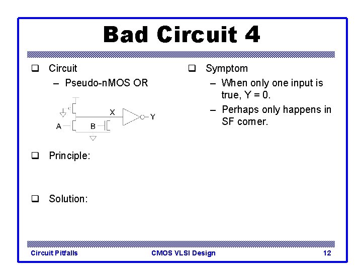
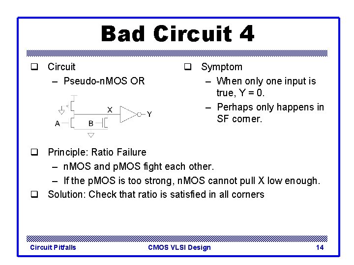
Bad Circuit 4 q Circuit – Pseudo-n. MOS OR q Symptom – When only one input is true, Y = 0. – Perhaps only happens in SF corner. q Principle: q Solution: Circuit Pitfalls CMOS VLSI Design 12

Bad Circuit 4 q Circuit – Pseudo-n. MOS OR q Symptom – When only one input is true, Y = 0. – Perhaps only happens in SF corner. q Principle: Ratio Failure – n. MOS and p. MOS fight each other. – If the p. MOS is too strong, n. MOS cannot pull X low enough. q Solution: Circuit Pitfalls CMOS VLSI Design 13

Bad Circuit 4 q Circuit – Pseudo-n. MOS OR q Symptom – When only one input is true, Y = 0. – Perhaps only happens in SF corner. q Principle: Ratio Failure – n. MOS and p. MOS fight each other. – If the p. MOS is too strong, n. MOS cannot pull X low enough. q Solution: Check that ratio is satisfied in all corners Circuit Pitfalls CMOS VLSI Design 14

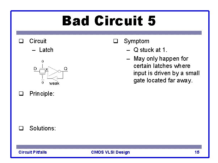
Bad Circuit 5 q Circuit – Latch q Symptom – Q stuck at 1. – May only happen for certain latches where input is driven by a small gate located far away. q Principle: q Solutions: Circuit Pitfalls CMOS VLSI Design 15

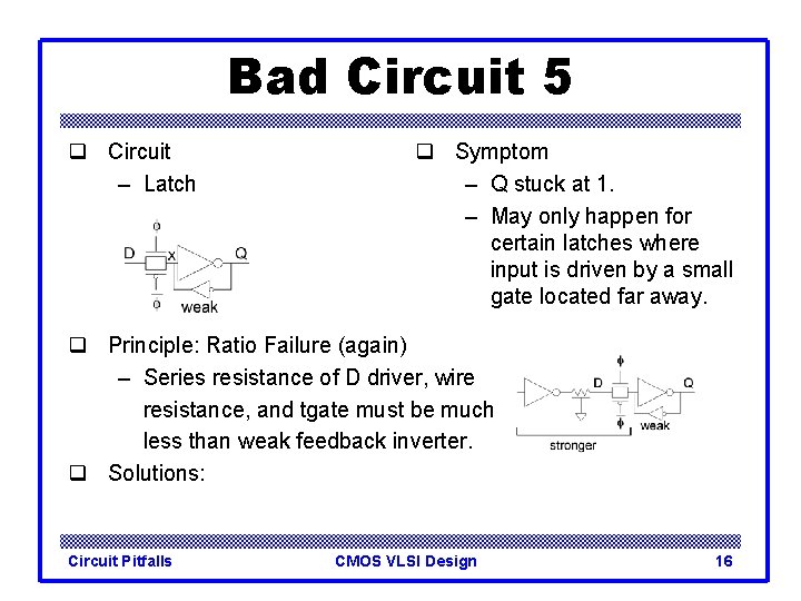
Bad Circuit 5 q Circuit – Latch q Symptom – Q stuck at 1. – May only happen for certain latches where input is driven by a small gate located far away. q Principle: Ratio Failure (again) – Series resistance of D driver, wire resistance, and tgate must be much less than weak feedback inverter. q Solutions: Circuit Pitfalls CMOS VLSI Design 16

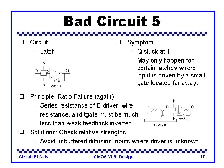
Bad Circuit 5 q Circuit – Latch q Symptom – Q stuck at 1. – May only happen for certain latches where input is driven by a small gate located far away. q Principle: Ratio Failure (again) – Series resistance of D driver, wire resistance, and tgate must be much less than weak feedback inverter. q Solutions: Check relative strengths – Avoid unbuffered diffusion inputs where driver is unknown Circuit Pitfalls CMOS VLSI Design 17

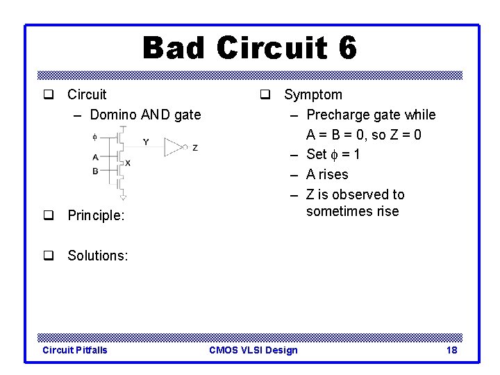
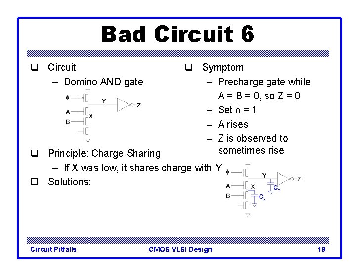
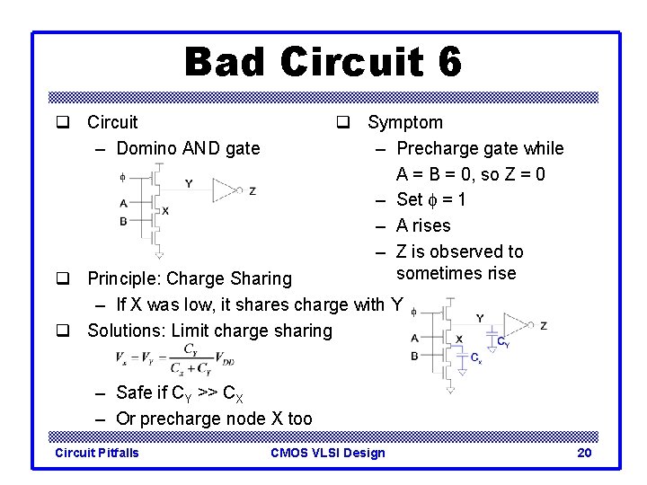
Bad Circuit 6 q Circuit – Domino AND gate q Principle: q Symptom – Precharge gate while A = B = 0, so Z = 0 – Set f = 1 – A rises – Z is observed to sometimes rise q Solutions: Circuit Pitfalls CMOS VLSI Design 18

Bad Circuit 6 q Circuit – Domino AND gate q Symptom – Precharge gate while A = B = 0, so Z = 0 – Set f = 1 – A rises – Z is observed to sometimes rise q Principle: Charge Sharing – If X was low, it shares charge with Y q Solutions: Circuit Pitfalls CMOS VLSI Design 19

Bad Circuit 6 q Circuit – Domino AND gate q Symptom – Precharge gate while A = B = 0, so Z = 0 – Set f = 1 – A rises – Z is observed to sometimes rise q Principle: Charge Sharing – If X was low, it shares charge with Y q Solutions: Limit charge sharing – Safe if CY >> CX – Or precharge node X too Circuit Pitfalls CMOS VLSI Design 20

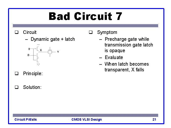
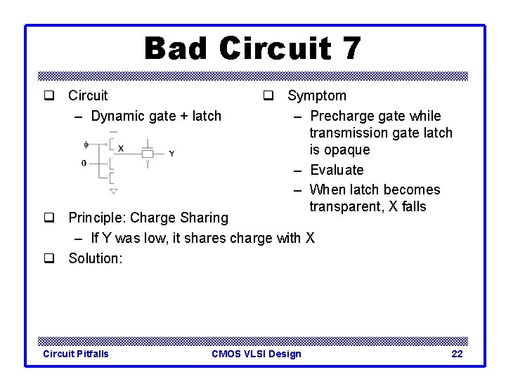
Bad Circuit 7 q Circuit – Dynamic gate + latch q Principle: q Symptom – Precharge gate while transmission gate latch is opaque – Evaluate – When latch becomes transparent, X falls q Solution: Circuit Pitfalls CMOS VLSI Design 21

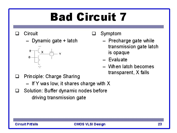
Bad Circuit 7 q Circuit – Dynamic gate + latch q Symptom – Precharge gate while transmission gate latch is opaque – Evaluate – When latch becomes transparent, X falls q Principle: Charge Sharing – If Y was low, it shares charge with X q Solution: Circuit Pitfalls CMOS VLSI Design 22

Bad Circuit 7 q Circuit – Dynamic gate + latch q Symptom – Precharge gate while transmission gate latch is opaque – Evaluate – When latch becomes transparent, X falls q Principle: Charge Sharing – If Y was low, it shares charge with X q Solution: Buffer dynamic nodes before driving transmission gate Circuit Pitfalls CMOS VLSI Design 23

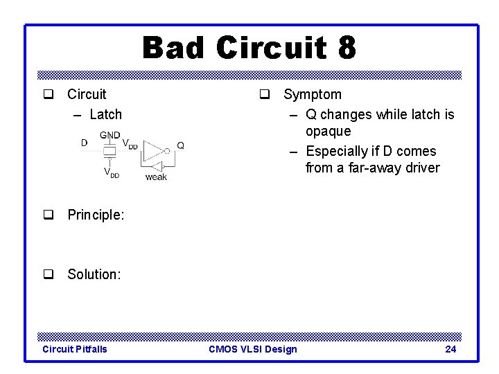
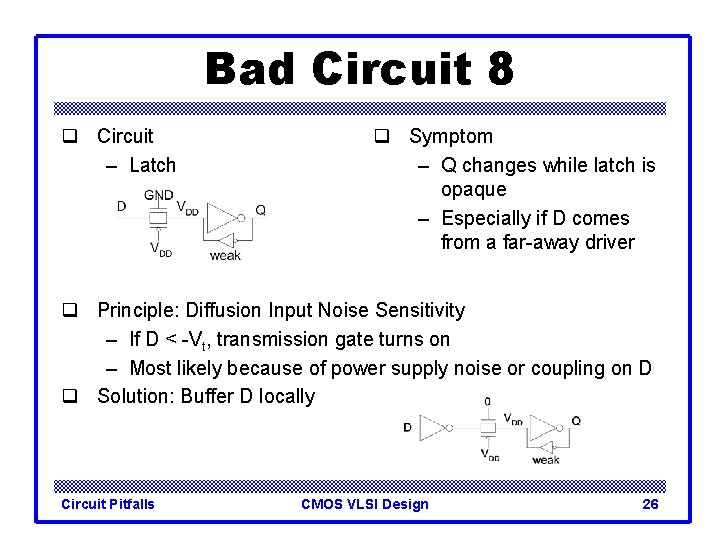
Bad Circuit 8 q Circuit – Latch q Symptom – Q changes while latch is opaque – Especially if D comes from a far-away driver q Principle: q Solution: Circuit Pitfalls CMOS VLSI Design 24

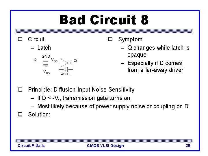
Bad Circuit 8 q Circuit – Latch q Symptom – Q changes while latch is opaque – Especially if D comes from a far-away driver q Principle: Diffusion Input Noise Sensitivity – If D < -Vt, transmission gate turns on – Most likely because of power supply noise or coupling on D q Solution: Circuit Pitfalls CMOS VLSI Design 25

Bad Circuit 8 q Circuit – Latch q Symptom – Q changes while latch is opaque – Especially if D comes from a far-away driver q Principle: Diffusion Input Noise Sensitivity – If D < -Vt, transmission gate turns on – Most likely because of power supply noise or coupling on D q Solution: Buffer D locally Circuit Pitfalls CMOS VLSI Design 26

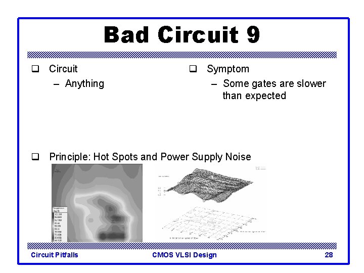
Bad Circuit 9 q Circuit – Anything q Symptom – Some gates are slower than expected q Principle: Circuit Pitfalls CMOS VLSI Design 27

Bad Circuit 9 q Circuit – Anything q Symptom – Some gates are slower than expected q Principle: Hot Spots and Power Supply Noise Circuit Pitfalls CMOS VLSI Design 28

Noise q Sources – Power supply noise / ground bounce – Capacitive coupling – Charge sharing – Leakage – Noise feedthrough q Consequences – Increased delay (for noise to settle out) – Or incorrect computations Circuit Pitfalls CMOS VLSI Design 29

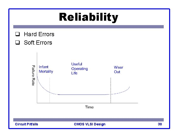
Reliability q Hard Errors q Soft Errors Circuit Pitfalls CMOS VLSI Design 30

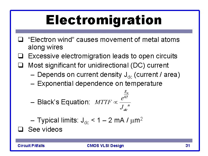
Electromigration q “Electron wind” causes movement of metal atoms along wires q Excessive electromigration leads to open circuits q Most significant for unidirectional (DC) current – Depends on current density Jdc (current / area) – Exponential dependence on temperature – Black’s Equation: – Typical limits: Jdc < 1 – 2 m. A / mm 2 q See videos Circuit Pitfalls CMOS VLSI Design 31

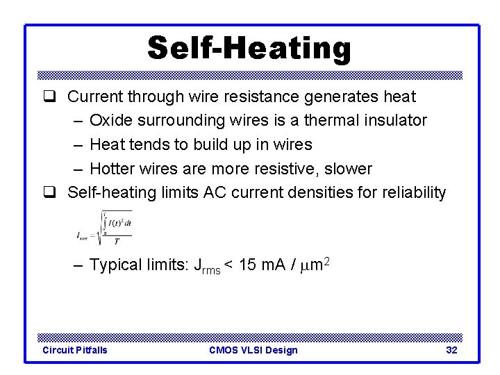
Self-Heating q Current through wire resistance generates heat – Oxide surrounding wires is a thermal insulator – Heat tends to build up in wires – Hotter wires are more resistive, slower q Self-heating limits AC current densities for reliability – Typical limits: Jrms < 15 m. A / mm 2 Circuit Pitfalls CMOS VLSI Design 32

Hot Carriers q E-field across channel impart high energies to some carriers – These “hot” carriers may be blasted into the gate oxide where they become trapped – Charge accumulation causes shift in Vt over time – Eventually Vt shifts too far for correct operation q Choose VDD to achieve reasonable product lifetime – Worst problems when substrate current is large – Highest current: saturated n. MOS devices • worst for inverters and NORs with fast input rise-time and long propagation delays Circuit Pitfalls CMOS VLSI Design 33

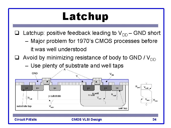
Latchup q Latchup: positive feedback leading to VDD – GND short – Major problem for 1970’s CMOS processes before it was well understood q Avoid by minimizing resistance of body to GND / VDD – Use plenty of substrate and well taps Circuit Pitfalls CMOS VLSI Design 34

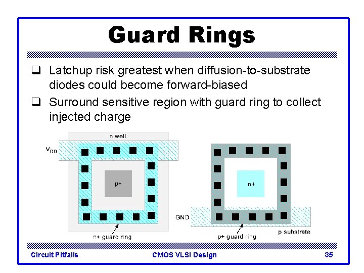
Guard Rings q Latchup risk greatest when diffusion-to-substrate diodes could become forward-biased q Surround sensitive region with guard ring to collect injected charge Circuit Pitfalls CMOS VLSI Design 35

Overvoltage q High voltages can damage transistors – Electrostatic discharge – Oxide arcing – Punchthrough – Time-dependent dielectric breakdown (TDDB) • Accumulated wear from tunneling currents q Requires low VDD for thin oxides and short channels q Use ESD protection structures where chip meets real world Circuit Pitfalls CMOS VLSI Design 36

Summary q Static CMOS gates are very robust – Will settle to correct value if you wait long enough q Other circuits suffer from a variety of pitfalls – Tradeoff between performance & robustness q Very important to check circuits for pitfalls – For large chips, you need an automatic checker. – Design rules aren’t worth the paper they are printed on unless you back them up with a tool. Circuit Pitfalls CMOS VLSI Design 37

Soft Errors q In 1970’s, DRAMs were observed to occasionally flip bits for no apparent reason – Ultimately linked to alpha particles and cosmic rays q Collisions with particles create electron-hole pairs in substrate – These carriers are collected on dynamic nodes, disturbing the voltage q Minimize soft errors by having plenty of charge on dynamic nodes q Tolerate errors through ECC, redundancy Circuit Pitfalls CMOS VLSI Design 38