VLSI Physical Design Automation Misc Topics and Conclusion
- Slides: 33
VLSI Physical Design Automation Misc. Topics and Conclusion Prof. David Pan dpan@ece. utexas. edu Office: ACES 5. 434 11/22/2020 1
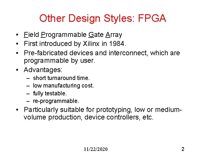
Other Design Styles: FPGA • Field Programmable Gate Array • First introduced by Xilinx in 1984. • Pre-fabricated devices and interconnect, which are programmable by user. • Advantages: – – short turnaround time. low manufacturing cost. fully testable. re-programmable. • Particularly suitable for prototyping, low or mediumvolume production, device controllers, etc. 11/22/2020 2
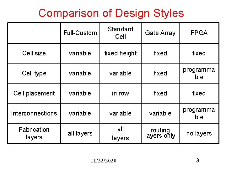
Comparison of Design Styles Full-Custom Standard Cell Gate Array FPGA Cell size variable fixed height fixed Cell type variable fixed programma ble Cell placement variable in row fixed Interconnections variable programma ble all layers routing layers only no layers Fabrication layers 11/22/2020 3
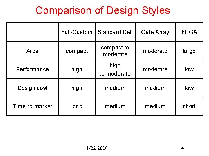
Comparison of Design Styles Full-Custom Standard Cell Gate Array FPGA Area compact to moderate large Performance high to moderate low Design cost high medium low Time-to-market long medium short 11/22/2020 4
Programming Technologies • • SRAM to control pass transistor / multiplexer EPROM – UV light Erasable PROM EEPROM – Electrically Erasable PROM Antifuses – One time programmable • They are different in ease of manufacturing, manufacturing reliability, area, ON and OFF resistance, parasitic capacitance, power consumption, re-programmability. 11/22/2020 5
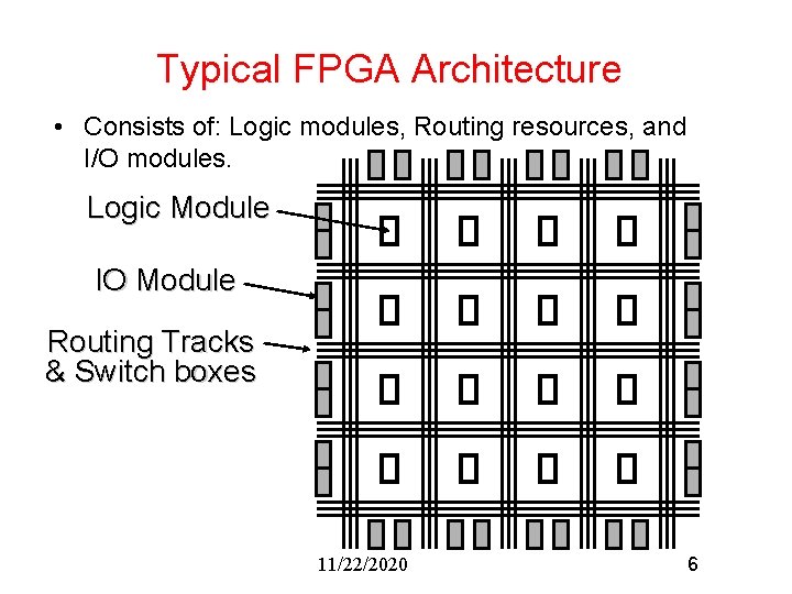
Typical FPGA Architecture • Consists of: Logic modules, Routing resources, and I/O modules. Logic Module IO Module Routing Tracks & Switch boxes 11/22/2020 6
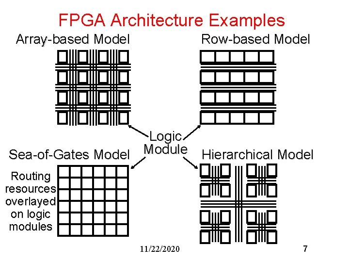
FPGA Architecture Examples Array-based Model Row-based Model Logic Sea-of-Gates Model Module Hierarchical Model Routing resources overlayed on logic modules 11/22/2020 7
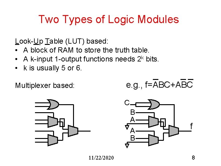
Two Types of Logic Modules Look-Up Table (LUT) based: • A block of RAM to store the truth table. • A k-input 1 -output functions needs 2 k bits. • k is usually 5 or 6. e. g. , f=ABC+ABC Multiplexer based: C B A A B 11/22/2020 f 8
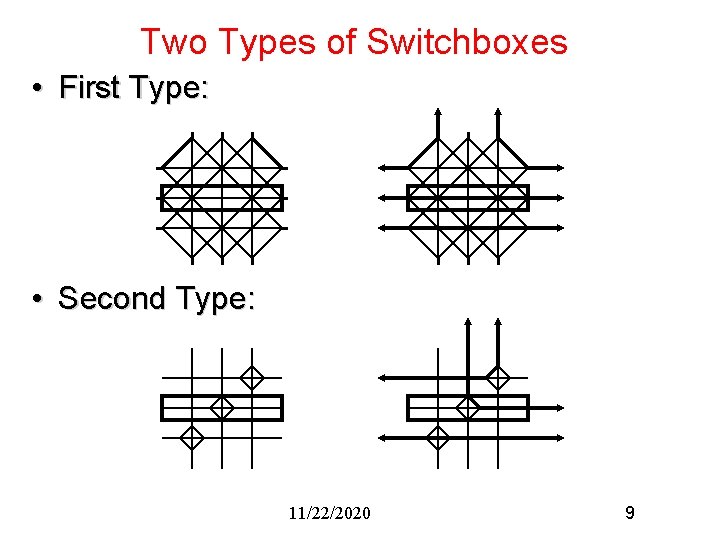
Two Types of Switchboxes • First Type: • Second Type: 11/22/2020 9
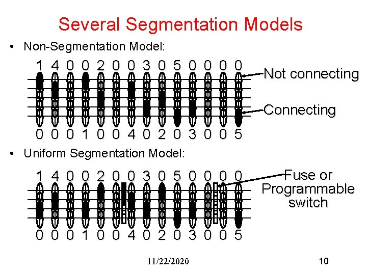
Several Segmentation Models • Non-Segmentation Model: 1 4 0 0 2 0 0 3 0 5 0 0 Not connecting Connecting 0 0 0 1 0 0 4 0 2 0 3 0 0 5 • Uniform Segmentation Model: 1 4 0 0 2 0 0 3 0 5 0 0 Fuse or Programmable switch 0 0 0 1 0 0 4 0 2 0 3 0 0 5 11/22/2020 10
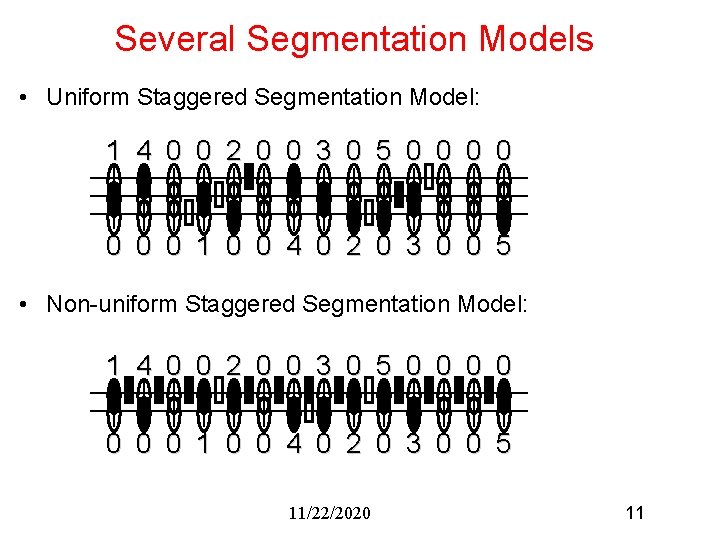
Several Segmentation Models • Uniform Staggered Segmentation Model: 1 4 0 0 2 0 0 3 0 5 0 0 0 0 1 0 0 4 0 2 0 3 0 0 5 • Non-uniform Staggered Segmentation Model: 1 4 0 0 2 0 0 3 0 5 0 0 0 0 1 0 0 4 0 2 0 3 0 0 5 11/22/2020 11
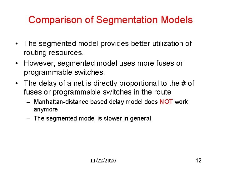
Comparison of Segmentation Models • The segmented model provides better utilization of routing resources. • However, segmented model uses more fuses or programmable switches. • The delay of a net is directly proportional to the # of fuses or programmable switches in the route – Manhattan-distance based delay model does NOT work anymore – The segmented model is slower in general 11/22/2020 12
Physical Design of FPGAs • Very different from other design styles • Architecture dependent: – – LUT or Multiplexer in logic modules Type of switchboxes used Type of segmentation model used. . . • Physical Design: – Partitioning – Floorplanning/Placement – Routing 11/22/2020 13
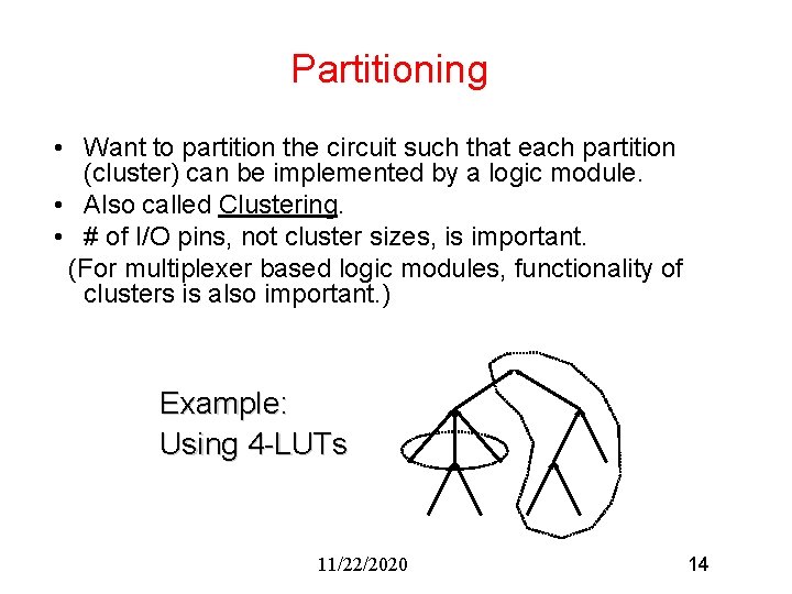
Partitioning • Want to partition the circuit such that each partition (cluster) can be implemented by a logic module. • Also called Clustering. • # of I/O pins, not cluster sizes, is important. (For multiplexer based logic modules, functionality of clusters is also important. ) Example: Using 4 -LUTs 11/22/2020 14
Placement • Assign clusters formed during partitioning to logic modules of FPGA. • The problem is the same as gate-array placement. 11/22/2020 15
Routing • Global routing: – Similar to global routing in other design styles. – Minimize wire length and balance densities. • Detailed routing: – Very different from other design styles. – Different algorithms for different segmentation models. – Channels and switchboxes have fixed capacities. 11/22/2020 16
Structured ASIC • New buzz word, but essentially gate array – Mask reconfigurable – Not field reconfigurable • Between FPGA and standard cells – Balance delay/performance and mask cost • Only programmable once – by vias (e. g. , Via-Programmable Gate Array – VPGA) 11/22/2020 17
Physcial Design Automation of MCMs and Si. Ps 11/22/2020 18
MCM and Si. P • Multi-Chip Module • System in package (Si. P) – Different package styles – Thermal consideration for 3 D • Alternative packaging approach for high performance systems. • Similar to PCB and IC layout problems, but – PCB layout tools cannot handle the dense and complex wiring structure of MCM. – IC layout tools cannot handle the complex electrical, thermal and geometrical constraints. 11/22/2020 19
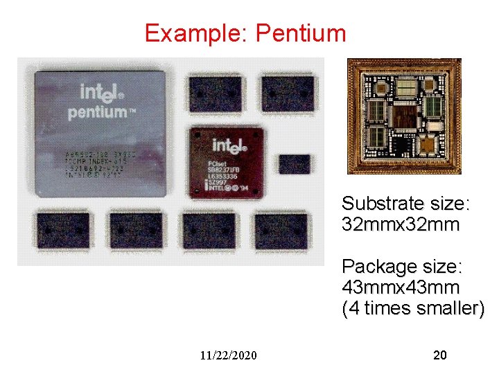
Example: Pentium Substrate size: 32 mmx 32 mm Package size: 43 mmx 43 mm (4 times smaller) 11/22/2020 20
Partitioning • Partitioning a circuit so that each sub-circuit can be implemented into a chip. • MCM may contain as many as 100 chips. • Need to consider timing constraints and thermal constraints • In addition, also need to consider traditional I/O constraints and area constraints. 11/22/2020 21
Placement • # of components is much less as compared to IC placement. • However, need to consider timing constraints and thermal constraints (as bare chips are placed close to each other). • Routing is done in routing layers, not between chips. • So no routing region needs to be allocated. 11/22/2020 22
Routing • Main objective is to satisfy timing constraints. • Another objective is to minimize # of routing layers, not to minimize routing area. – Cost is directly proportional to # of layers • Crosstalk, skin effect and parasitic effect are important considerations. • Wires are of smaller pitch and more dense than PCB layout. 11/22/2020 23
EE 382 V -- Conclusions 11/22/2020 24
What Have Been Taught? • Introduced different problems in Physical Design. • Numerous algorithms which are different in terms of – – – – design styles objectives constraints techniques optimality efficiency robustness. . . 11/22/2020 25
What Is Important? • Understand the problems – How to formulate the problems, represent the constraints, solutions, etc. – Reasonable assumptions/abstractions • Know fundamental algorithms to solve the problems. • However, the world keeps on changing: – – – technology objectives constraints requirement on solution quality computational power • It is more important to learn how to think – formulate the problem – solve it smartly 11/22/2020 26
Problem Solving Techniques • Greedy Algorithm • Simulated Annealing/Genetic Algorithm • Mathematical Programming – Linear, Quadratic, Integer Linear, geometric, posynomial, … • Dynamic Programming • Reduction to graph problems – min-cut, max-cut, shortest path, longest path, bipartite matching, minimum spanning tree, etc. • Divide-and-Conquer • Many different heuristics • . . 11/22/2020 27
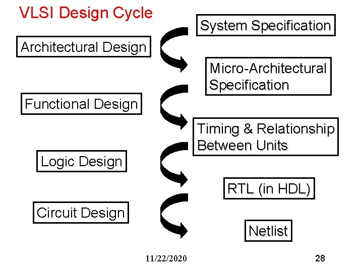
VLSI Design Cycle System Specification Architectural Design Micro-Architectural Specification Functional Design Timing & Relationship Between Units Logic Design RTL (in HDL) Circuit Design Netlist 11/22/2020 28
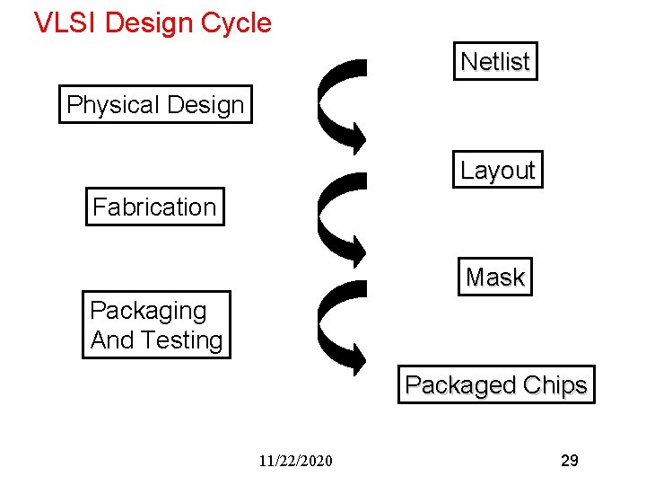
VLSI Design Cycle Netlist Physical Design Layout Fabrication Mask Packaging And Testing Packaged Chips 11/22/2020 29
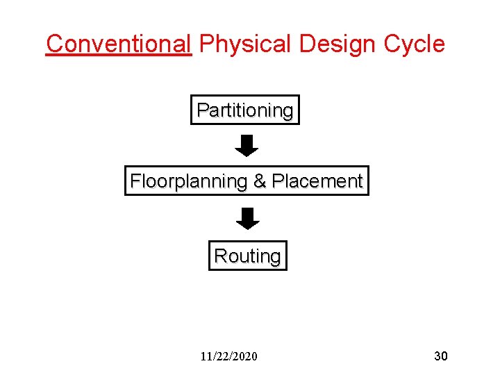
Conventional Physical Design Cycle Partitioning Floorplanning & Placement Routing 11/22/2020 30
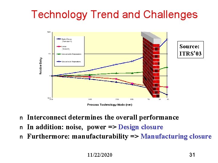
Technology Trend and Challenges Source: ITRS’ 03 n n n Interconnect determines the overall performance In addition: noise, power => Design closure Furthermore: manufacturability => Manufacturing closure 11/22/2020 31
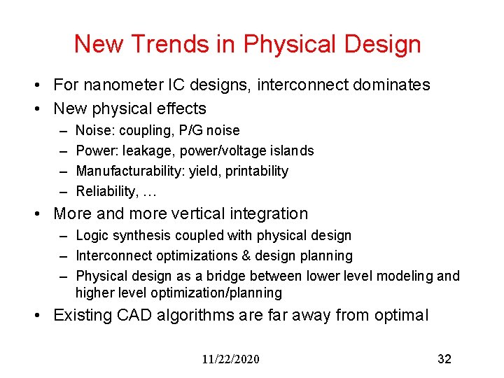
New Trends in Physical Design • For nanometer IC designs, interconnect dominates • New physical effects – – Noise: coupling, P/G noise Power: leakage, power/voltage islands Manufacturability: yield, printability Reliability, … • More and more vertical integration – Logic synthesis coupled with physical design – Interconnect optimizations & design planning – Physical design as a bridge between lower level modeling and higher level optimization/planning • Existing CAD algorithms are far away from optimal 11/22/2020 32
Check points ü Problem solving skills on underlying physical design algorithms ü Know what’s behind the scene of CAD tools ü Know the trend and critique ability if given a new research paper ü Project study of a topic of your choice and implementation (through class project) ü Presentation skill ü Paper writing and job preparation 11/22/2020 33