CS 612 Algorithms for Electronic Design Automation Course



- Slides: 16

CS 612 Algorithms for Electronic Design Automation Course Overview Mustafa Ozdal CS 612 – Lecture 1 Mustafa Ozdal Computer Engineering Department, Bilkent University 1

What is EDA? Stands for Electronic Design Automation � a. k. a VLSI CAD Software tools to support engineers in the creation of new IC designs. EDA tools significantly reduce the cost and time-tomarket of new projects. �A CPU can easily contain > 1 B transistors in a single chip � Manual design is prohibitive CS 612 – Lecture 1 Mustafa Ozdal Computer Engineering Department, Bilkent University 2

What is EDA? Solves a wide-range of problems high-level system design to fabrication (and everything in between) Strong software skills required This course will cover the physical design problems � Abstract and algorithmic problems � No EE knowledge needed CS 612 – Lecture 1 Mustafa Ozdal Computer Engineering Department, Bilkent University 3

Why Study EDA Algorithms? You may consider a career in the EDA field EDA companies: Synopsys, Cadence, Mentor Graphics, … � Design companies: Intel, IBM, Apple, AMD, Nvidia, TI, Qualcomm, ARM, TSMC, … � You may be working in a related field e. g. Computer architecture: What is the hardware cost, energy cost, etc. of a new feature? � e. g. Scientific computing: Common algorithms used in both domains (e. g. graph partitioning, clustering, etc. ) � You may want to improve your algorithmic skills � We will study algorithms for abstract problems that also occur in other domains. e. g. routing, rectangle packing, partitioning, etc. CS 612 – Lecture 1 Mustafa Ozdal Computer Engineering Department, Bilkent University 4

Course Overview Schedule: Lecture: Spare Hour: Tue. 13: 40 -14: 30 Thu. 15: 40 -17: 30 Tue. 14: 40: 15: 30 EA 502 Course project: More in-depth study of a topic � Literature survey + implementation + experiments � Presentation (survey + plans) � Final report (implementation + experiments + conclusions) CS 612 – Lecture 1 Mustafa Ozdal Computer Engineering Department, Bilkent University 5

Sneak Preview of the Problems CS 612 – Lecture 1 Mustafa Ozdal Computer Engineering Department, Bilkent University 6

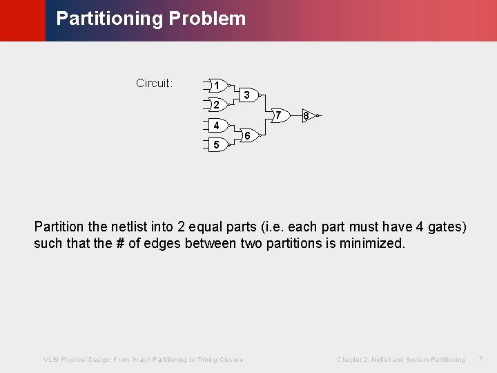
© KLMH Partitioning Problem Circuit: 1 2 4 5 3 7 8 6 VLSI Physical Design: From Graph Partitioning to Timing Closure Chapter 2: Netlist and System Partitioning 7 Lienig Partition the netlist into 2 equal parts (i. e. each part must have 4 gates) such that the # of edges between two partitions is minimized.

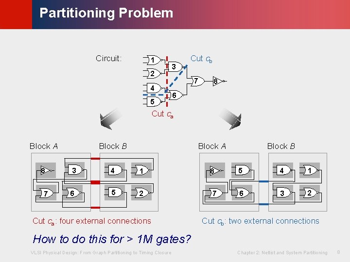
© KLMH Partitioning Problem Circuit: 1 2 4 5 3 Cut cb 7 8 6 Cut ca Block A 8 7 Block B Block A 3 4 1 6 5 2 Cut ca: four external connections 8 7 Block B 5 4 1 6 3 2 Cut cb: two external connections VLSI Physical Design: From Graph Partitioning to Timing Closure Chapter 2: Netlist and System Partitioning 8 Lienig How to do this for > 1 M gates?

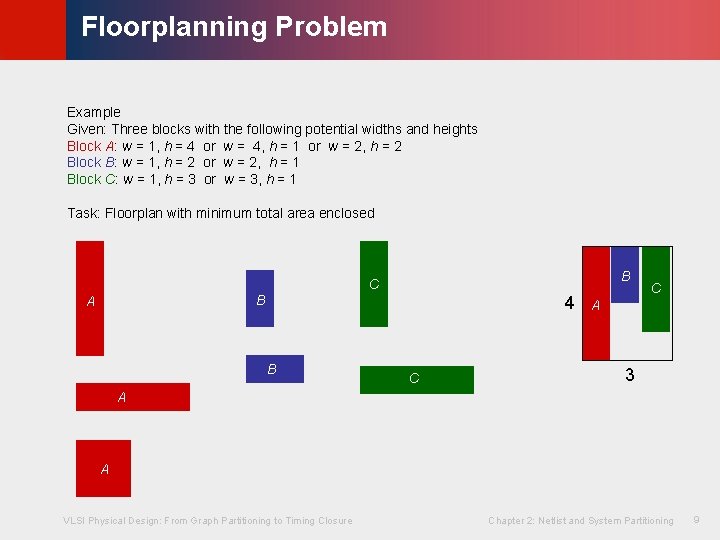
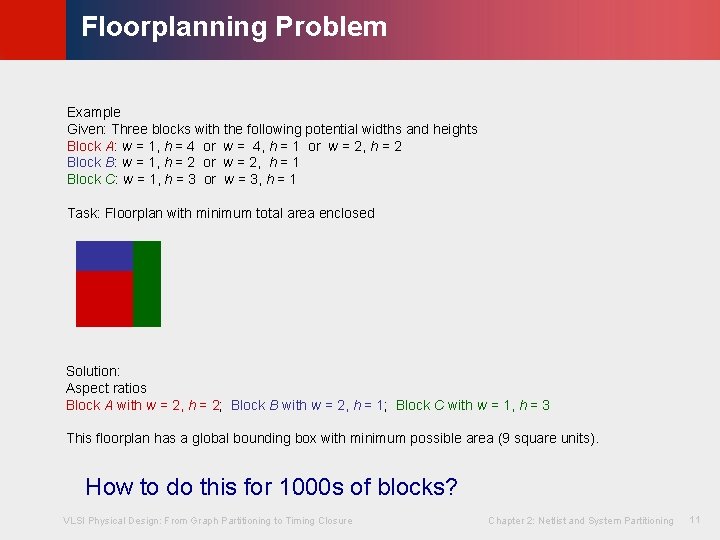
© KLMH Floorplanning Problem Example Given: Three blocks with the following potential widths and heights Block A: w = 1, h = 4 or w = 4, h = 1 or w = 2, h = 2 Block B: w = 1, h = 2 or w = 2, h = 1 Block C: w = 1, h = 3 or w = 3, h = 1 Task: Floorplan with minimum total area enclosed B C B A 4 B C C A 3 A VLSI Physical Design: From Graph Partitioning to Timing Closure Chapter 2: Netlist and System Partitioning 9 Lienig A

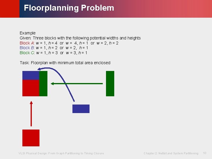
© KLMH Floorplanning Problem Example Given: Three blocks with the following potential widths and heights Block A: w = 1, h = 4 or w = 4, h = 1 or w = 2, h = 2 Block B: w = 1, h = 2 or w = 2, h = 1 Block C: w = 1, h = 3 or w = 3, h = 1 VLSI Physical Design: From Graph Partitioning to Timing Closure Chapter 2: Netlist and System Partitioning 10 Lienig Task: Floorplan with minimum total area enclosed

© KLMH Floorplanning Problem Example Given: Three blocks with the following potential widths and heights Block A: w = 1, h = 4 or w = 4, h = 1 or w = 2, h = 2 Block B: w = 1, h = 2 or w = 2, h = 1 Block C: w = 1, h = 3 or w = 3, h = 1 Task: Floorplan with minimum total area enclosed Solution: Aspect ratios Block A with w = 2, h = 2; Block B with w = 2, h = 1; Block C with w = 1, h = 3 This floorplan has a global bounding box with minimum possible area (9 square units). VLSI Physical Design: From Graph Partitioning to Timing Closure Chapter 2: Netlist and System Partitioning 11 Lienig How to do this for 1000 s of blocks?

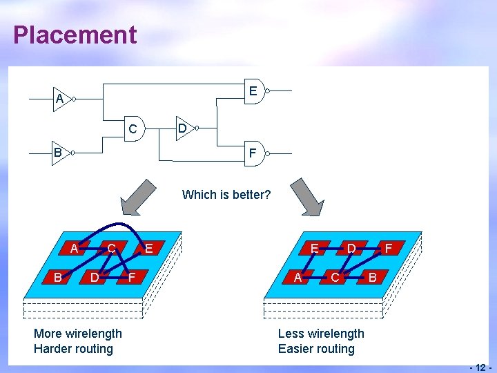
Placement E A D C B F Which is better? A B C D More wirelength Harder routing E F E A D C F B Less wirelength Easier routing - 12 -

Placement as an Optimization Problem Place all cells in the netlist such that: Minimize chip area Minimize wire length Make routing easy Satisfy timing constraints Keep cells on critical paths closer Satisfy various other design constraints A typical design can have > 1 M cells NP-complete problem - 13 -

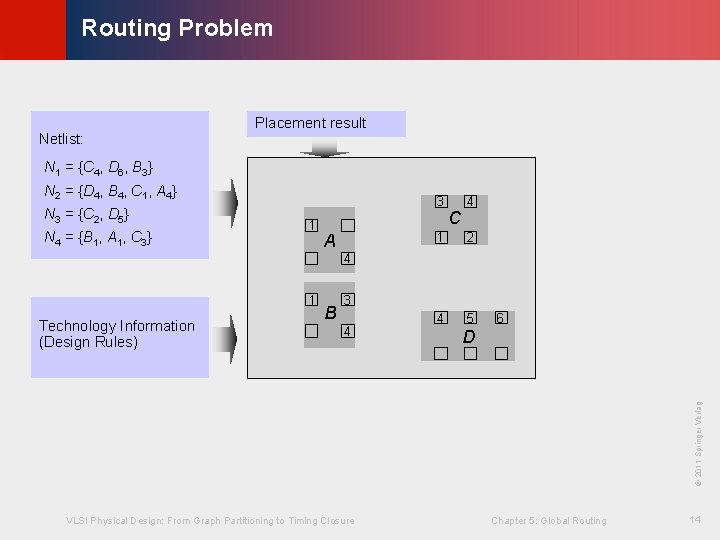
© KLMH Routing Problem Netlist: Placement result N 1 = {C 4, D 6, B 3} N 2 = {D 4, B 4, C 1, A 4} N 3 = {C 2, D 5} N 4 = {B 1, A 1, C 3} 3 1 A C 4 1 2 4 5 4 1 3 4 6 D VLSI Physical Design: From Graph Partitioning to Timing Closure Chapter 5: Global Routing 14 Lienig © 2011 Springer Verlag Technology Information (Design Rules) B

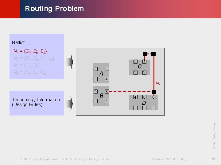
© KLMH Routing Problem Netlist: N 1 = {C 4, D 6, B 3} N 2 = {D 4, B 4, C 1, A 4} N 3 = {C 2, D 5} N 4 = {B 1, A 1, C 3} 3 1 A 1 C 4 2 4 1 3 4 4 5 6 D VLSI Physical Design: From Graph Partitioning to Timing Closure Chapter 5: Global Routing 15 Lienig © 2011 Springer Verlag Technology Information (Design Rules) B N 1

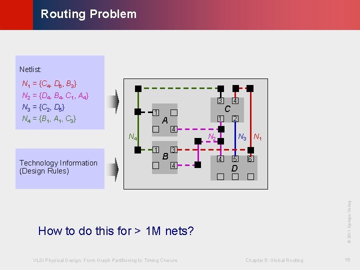
© KLMH Routing Problem Netlist: N 1 = {C 4, D 6, B 3} N 2 = {D 4, B 4, C 1, A 4} 3 N 4 = {B 1, A 1, C 3} A 4 N 4 1 Technology Information (Design Rules) 1 B C 2 N 3 N 1 3 4 4 5 6 D © 2011 Springer Verlag 1 4 How to do this for > 1 M nets? VLSI Physical Design: From Graph Partitioning to Timing Closure Chapter 5: Global Routing 16 Lienig N 3 = {C 2, D 5}